MITEL NWK914GP1N, NWK914CG, NWK914D Datasheet

PHY/PMD High Speed Copper Media Transceiver
The NWK914D is a Physical Layer device designed for
use in 100BASE-TX applications. The NWK914D has
integrated the 100mb/s transceiver, clock and data recovery
and NRZI conversion circuitry. It is designed for use in cost
effective NIC adapter cards and 100BASE-TX repeater and
switch applications.
The device connects through a 5 bit symbol interface
directly with any MAC controller that includes the PCS layer,
resulting in a simple and cost effective solution. It will also
interface with a PCS device such as the NWK935 to form a
complete 100BASE-TX Physical Layer for connection to the
IEEE 802.3 standard MII interface.
FEATURES
■ Compatible with IEEE-802.3 Standards
■ Operates over 100 Meters of STP and Category 5
UTP cable
■ Five Bit TTL Level Symbol Interface
■ Integrated Clock and Data Recovery
■ Supports Full-duplex Operation
■ Integral 10 Mb/s Buffer for Dual 10 Mb/s & 100 Mb/s
Applications
■ Adaptive Equalization
■ 25MHz to 125MHz Transmit Clock Multiplier
■ Programmable TX Output Current
■ Base Line Wander Correction
Preliminary Information
RDAT4
RDAT3
RDAT2
RDAT1
RDAT0
TXC
48
RXIP
RXIN
49
CC
EQSEL
RXV 1
47
10TXIN
525150
1
TTLGND
2
N/C
3
N/C
4
RXC
5
SDT
RDLV
6
CC
7
N/C
N/C
RXPLLV
RXV
LFRB
LFRA
8
9
10
11
12
CC
13
CC
14151617181920
RXGND
RXPLLGND
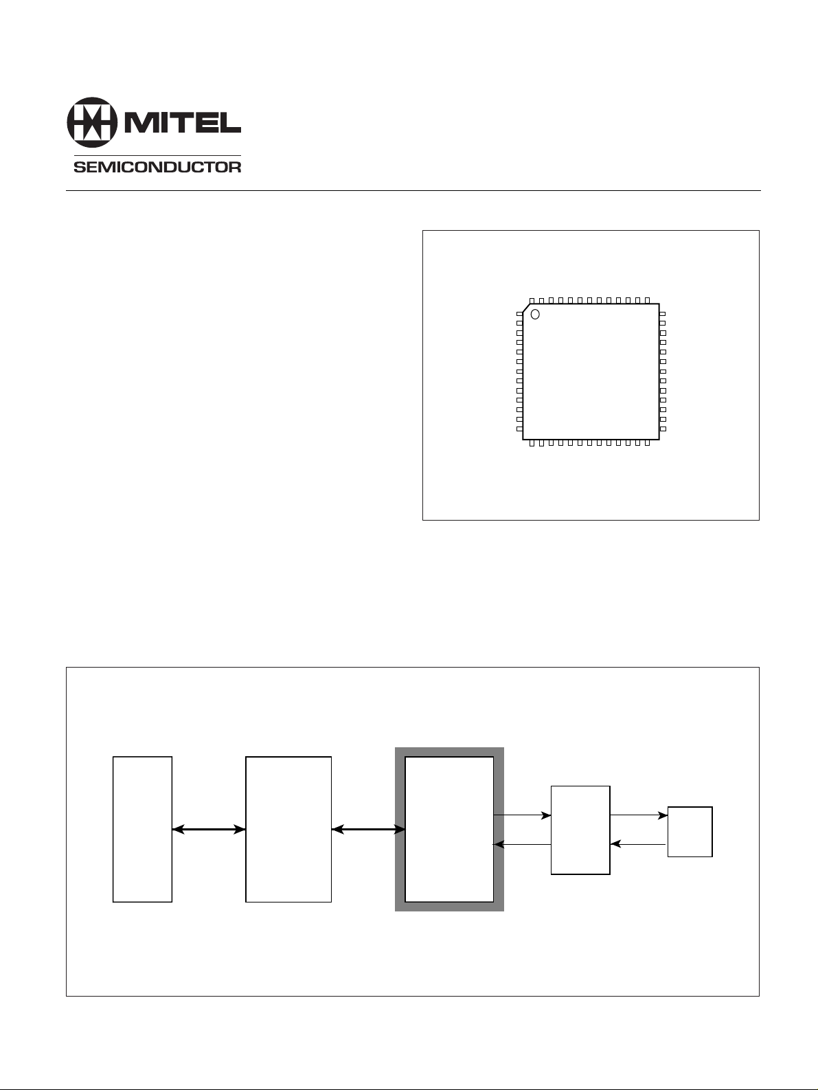
Fig.1 Pin connections - top view
■ Single +5V supply
■ 52 Pin PQFP package
ORDERING INFORMATION
NWK914D/CG/GP1N
NWK914D
NWK914D
DS4829 - 1.1 December 1997
CC
TTLV
REFCLK
TDAT0
TDAT1
TDAT2
TDAT3
22
TXON
23
TXOP
242526
TXREF
TXGND
TDAT4
CC
BGAPV
39
TTLGND
TEST
38
TESTIP
37
N10/100
36
LBEN
35
TDLV
34
33
TXOE
32
TXPLLV
31
LFTA
30
LFTB
29
TXPLLGND
28
BGAPGND
27
SUBGND
CC
CC
GP52
46454443424140
21
CC
TXV
10TXIP
MAC or
Repeater
Controller
IC
MII
Interface
NWK935
100 PCS
Symbol
Interface
NWK914D
Fig.2 Simplified system diagram
Isolation
Magnetics
RJ-45
1

NWK914D
ABSOLUTE MAXIMUM RATINGS
Operation at absolute maximum ratings is not implied.
Exposure to stresses outside those listed could cause
permanent damage to the device.
DC Supply voltage (V
) -0.5 to +7V
CC
RECOMMENDED OPERATING CONDITIONS
DC supply voltages (VCC) +5V ±5%
Operating temperature (TA)0°C to +70°C (+25°C typ.)
Power dissipation (P
) 750mW (typ.)
D
Storage temperature (tst) -65 to +150°C
ESD 2kV HBM
ELECTRICAL CHARACTERISTICS
Recommended operating conditions apply except where stated.
Characteristic Symbol Units Conditions
Min. Typ. Max.
DC characteristics
Total V
TTL high level I/P voltage V
supply current I
CC
TTL low level I/P voltage V
TTL high level I/P current I
TTL low level I/P current I
EQSEL high level I/P voltage V
EQSEL low level I/P voltage V
EQSEL floating level I/P V
EQSEL high level I/P current I
EQSEL low level I/P current I
TTL high level O/P voltage V
TTL low level O/P voltage V
TTL high level O/P current I
TTL low level O/P current I
CC
IH
IL
IH
IL
IH
IL
IZ
IH
IL
OH
OL
OH
OL
- 150 - mA device only
2--V
- - 0.8 V
--20µAVIH = V
- - –400 µAVIL = 0.4V
4.2 - - V
- - 0.8 V
-V
- - 1400 µAVIH = V
- - –1400 µAVIL = 0V
2.4 - - V IOH = 20µA
- - 0.5 V IOL = 4mA
- - –200 µA
--4mA
Transmit O/P current - 40 - mA R
pins TXOP, TXON 100Mb/s data
Differential RX I/P - 1.4 - Vp-p measured on device pins
signal voltage 100Mb/s data, 0mCable
RX I/P common mode voltage - V
RX I/P impedance - 24 - kΩ
Signal detect threshold V
TH
- 50 - % wrt normalized output of
Low voltage shutdown - 3.8 - V
Value
/2 - V
CC
= 1300Ω
REF
/2 - V RX I/Ps floating
CC
equalizer
CC
CC
PLL characteristics
3dB bandwidth - 50 - kHz
Damping factor - 2 Peaking - - .005 dB
Overshoot - - 5 %
Static error - ±0.5 - ns
Jitter - - 0.5 ns
VCO characteristics
Centre frequency - 125 - MHz
Deviation - ±40 - MHz
Gain @125MHz - 70 - MHz/V
2

NWK914D
REFCLK
TXC
TDAT0
TDAT1
TDAT2
TDAT3
TDAT4
BGAPV
BGAPGND
RXC
RDAT0
RDAT1
RDAT2
RDAT3
RDAT4
10T
LFTB
LFTATTLV
CC
TIMES FIVE
CLOCK
MULTIPLIER
SHIFTER &
NRZ to NRZI
CC
SHIFTER &
NRZI to NRZ
TTLGND1
DIVIDE
CLOCK
by FIVE
TTLGND2 LFRB
125
MHz
RXPLLV
CLOCK
RECOVERY
PLL,125MHZ
LFRA
TXPLLV
CC
LOW VOLTAGE
SHUT DOWN
BAND GAP
VOLTAGE
REFERENCE
CC
SDT
TXOE
TXREF
CURRENT
REFERENCE
NRZI
to
MLT-3
COMPARATORS
MLT-3 to NRZI
TTL
IN 10TXIP
X
SIGNAL
DETECT
ADAPTIVE
EQUALIZER
TXPLLGNDRXPLLGND
TDLV
TESTIP
CC
100
Mb/s
LEVEL
N10/100
10
Mb/s
3
TEST
TTL
RDLV
CC
TXV
CC
TXOP
TXON
TXGND
LBEN
EQSEL
RXIP
RXIN
2
RXV
CC
RXVCC1
RXGND
SUBGND
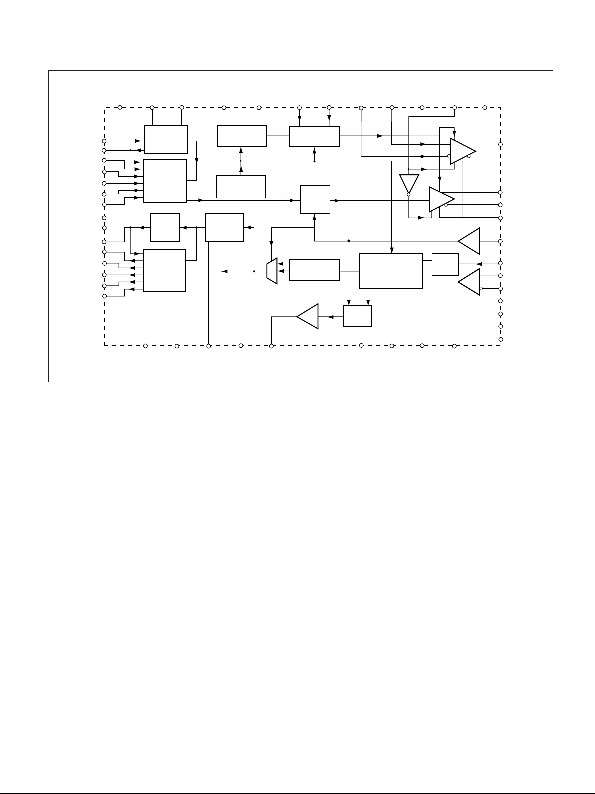
Fig.3 System block diagram
FUNCTIONAL DESCRIPTION
The functional blocks within the device are shown in Fig. 3.
These are described below:-
Transmit Section
Times Five Clock Multiplier 25MHz to 125MHz
This circuit consists of a phase lock loop (PLL) that is
operating at 125MHz, centre frequency. The 125MHz is
divided by 5 to produce a 25MHz clock which is phase
compared with a 25MHz crystal clock reference frequency
which is input on pin REFCLK. The 25MHz clock (pin TXC)
is then sent to the PCS layer to clock in in the 5 bit nibble
data. Pins LFTA and LFTB are provided to set the VCO
characteristics. The recommended loop filter components
are shown in Fig.6.
A control current is derived from the clock multiplier and
is used by the receive clock recovery circuit to centre the
PLL when no input data is present.
Five Bit Nibble to 125MHz Shifter
Data is input to the transmit side in 5 bit wide parallel
form on pins TDAT0 through TDAT4. This NRZ data is
clocked in on the positive edge of the 25MHz clock pin TXC.
The parallel data is first loaded into a 5 bit wide register prior
to being loaded into a 5 bit PISO where it is converted into
a serial data stream. The last stage of the shifter incorporates
a converter to change the data from NRZ to NRZI.
NRZ to MLT3 Encoder
The serial data from the shifter then passes through an
encoder which converts the NRZI binary data into the three
level MLT-3 format for transmission by the 'TXO' outputs.
Transmit Line Drivers
There are two on-chip Line Drivers both of which share
the output pins TXOP and TXON. The N10/100 pin is used
to control which driver is active and allowed to drive the line.
When held high the MLT-3 data is output by the 100Mb/s
driver. This driver consists of differential current source
outputs with programmable sink capability, designed to
drive a nominal output impedance of 50Ω.
Output current is set by the value of an external resistor
) between pin 'TXREF' and 'TXGND'.
(R
REF
This resistor defines an internal reference current derived
from an on-chip bandgap reference.
Final output current at the 'TXO' outputs is a multiple of
this current and is defined as:-
I
(mA) = 52/R
TXO
REF
(kΩ)
Transition times of the 'TXO' outputs are matched and
internally limited to approx. 2.5ns to reduce EMI emissions.
3
 Loading...