MITEL NJ88C33MAMP, NJ88C33MADP Datasheet

Frequency Synthesiser (I2C BUS Programmable)
The NJ88C33 is a synthesiser circuit fabricated on Mitel
Semiconductor's 1.4 micron CMOS process, assuring very
high performance. It is I2C compatible and can also be
programmed at up to 5MHz. It contains a 16-bit R counter, a
12-bit N counter and a 7-bit A counter.
A digital phase comparator gives improved loop stability
with current source outputs to reduce loop components. A
voltage doubler is provided for the loop driver to improve
control voltage range to the VCO when operating at low supply
voltages.
FEATURES
■ Easy to Use
■ Low Power Consumption (15mW)
■ Single Supply 2.5V to 5.5V
■ Digital Phase Comparator with Current Source
Outputs
■ Serial (I2C Compatible) Programming, 5MHz max
■ Channel Loading in 8µs
■ 150MHz Input Frequency Without Prescaler at 4.5V
(52MHz at 2.7V)
■ Standby Modes
■ Use of Two-Modulus Prescaler is Possible
APPLICATIONS
■ Cordless Telephones (CT2, DECT)
■ Cellular Telephones (GSM, PCN, ETACS)
■ Hand Held Marine Radios
■ Sonarbuoys
■ Video Clock generators
NJ88C33
Advance Information
DS2429 - 3.2 September 1994
DP14
MP14
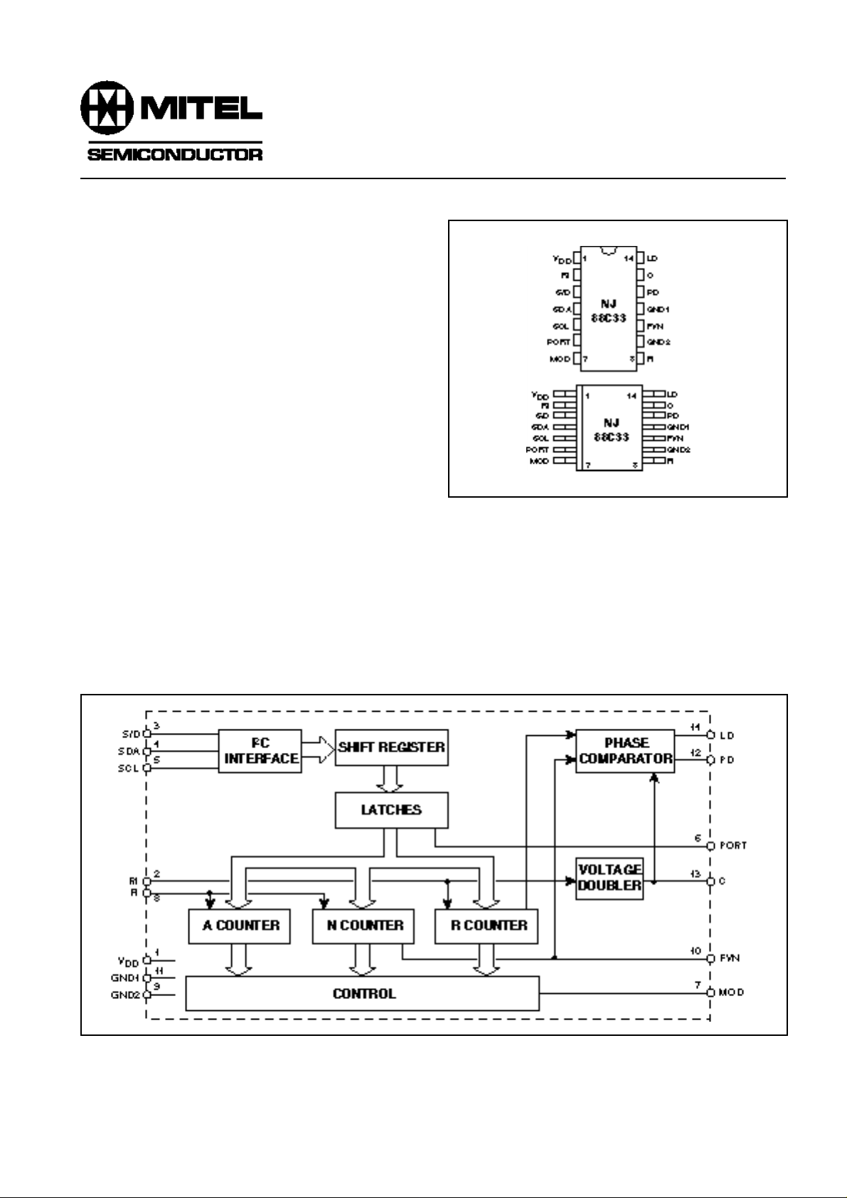
Fig.1 Pin connections (not to scale) - top views
ABSOLUTE MAXIMUM RATINGS
Supply voltage, V
Input voltage, V
Output voltage on pin 13, V
Storage temperature, T
DD
IM1
IM2
stg
ORDERING INFORMATION
NJ88C33 MA DP (Industrial - Plastic DIL package)
NJ88C33 MA MP (Industrial - Miniature Plastic DIL package)
-0.3V to 7V
-0.3 to VDD +0.3V
-VDD to 0V
-55°C to +125°C
Fig.2 Simplified block diagram of NJ88C33

NJ88C33
PIN DESIGNATIONS
Pin
No.
1
2
Pin
Name
V
DD
RI
Description
Supply voltage (normally 5V or 3V).
Reference frequency input from an accurate source, normally a crystal oscillator. The input is normally
an AC coupled sinewave but may be a DC coupled square wave.
10
11
12
13
3
S/D
Single/dual modulus operating mode selection input. Single modulus operation is selected by driving
the pin low. 'High' selects dual modulus mode.
4
5
6
SDA
SCL
PORT
I2C bus data input pin. It is also an open-drain output for generating I2C bus acknowledge pulses.
I2C bus clock input. It can be clocked at up to 5MHz.
Output control pin, which can be programmed via the I2C bus. It can be connected to the S/D pin to
select single or dual modulus mode under bus control.
7
MOD
Modulus control pin. It is high in single modulus mode but switches in dual modulus operation. In dual
modulus mode, MOD remains low during operation of the A counter until A=0; MOD then remains high
until N=0, when both counters are reloaded. It can be programmed via the I2C bus as an open-drain
or push-pull output.
8
FI
Frequency input from a VCO or prescaler. The input is normally an AC coupled sinewave but may be
a DC coupled square wave.
9
GND2
Dedicated ground for the FI input buffer. It should be connected to the VCO ground or the prescaler
ground, if used. Any noise on this pin will affect the performance of the VCO loop.
FVN
GND1
PD
Open-drain output from the N counter.
Ground supply pin (global).
Tristate current output from the phase detector. The polarity of the output can be programmed via the
I2C bus.
C
Voltage doubler output. The operation of the doubler can be controlled via the I2C bus. In applications
where the voltage doubler is switched off, this pin should be connected to GND1; a reservior capacitor
should be connected from this pin to GND1 for applications where it is switched on.
14
LD
Open-drain lock detect output - requires integration if used.
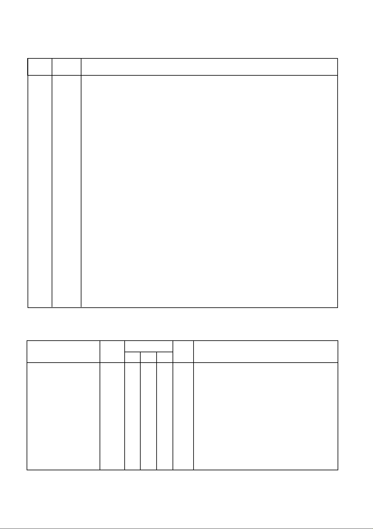
OPERATING RANGE
Test conditions (unless otherwise stated):
PLL locked, RI = 10MHz
Characteristic
Supply voltage
Ambient temperature
Supply current
Single modulus
Dual modulus
Standby mode
Standby mode
Symbol
V
DD
T
amb
I
DD
I
DD
I
DD
I
DD
Min.
2.5
-40
Value
Typ. Max.
5.5
5
+85
3.0
2.1
3.0
2
1.5
1.0
Unit
Conditions
V
°C
FI = 50MHz, VFI = 150mVrms, N,R > 1000 without
mA
voltage doubler, VDD = 5V, T
FI = 10MHz, VFI = 500mVrms, N,R > 1000 without
mA
voltage doubler, VDD = 5V, T
µA
1
FI = 50MHz, VFI = 150mVrms, preamp off, divider off,
VDD = 5V, T
mA
FI = 50MHz, VFI = 150mVrms, preamp on, divider off,
VDD = 5V, T
amb
amb
= 25°C
= 25°C
amb
amb
= 25°C
= 25°C
2

NJ88C33
3

NJ88C33
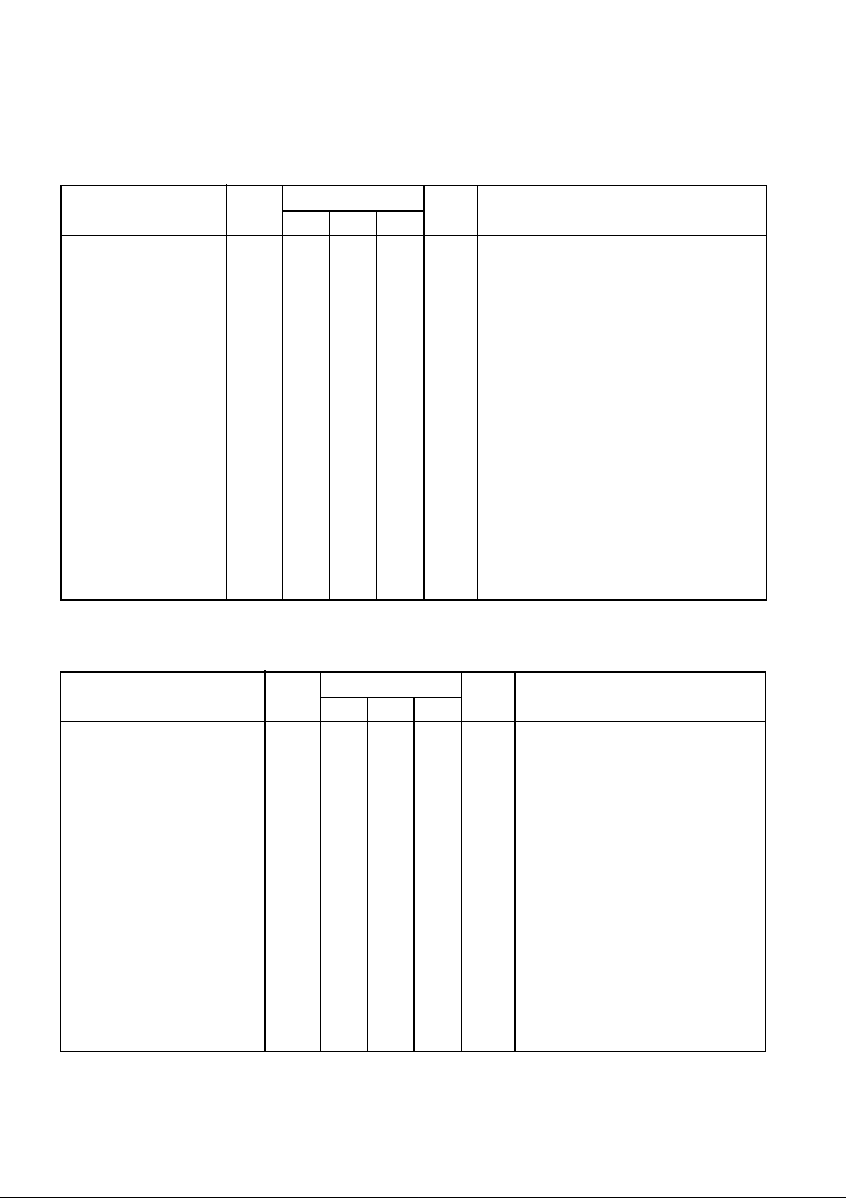
ELECTRICAL CHARACTERISTICS
These characteristics are guaranteed over the following conditions (unless otherwise stated):
VDD = 4.5V to 5.5V, T
INPUT SIGNALS
= -40°C to +85°C
amb
Characteristic
Symbol
Min.
Value
Unit
Conditions
Max.Typ.
Input Signals SDA,
SCL, S/D
Input voltage high
Input voltage low
Input capacitance
Input current
V
V
C
I
0.7V
IH
IL
I
IN
DD
0
V
0.3V
10
10
DD
V
V
DD
pF
VIN = VDD = 5.5V
µA
Input signal RI
Input frequency
Input voltage
Input capacitance
Input current
Input signal FI
Input frequency
Input voltage
Input capacitance
Input current
Input signal FI
Input frequency
Input voltage
Input capacitance
Input current
f
max
V
Irms
C
I
I
IN
f
max
V
Irms
C
I
I
IN
f
max
V
Irms
V
Irms
V
Irms
C
I
I
IN
100
50
30
100
200
52
10
10
52
10
10
150
10
10
MHz
MHz
MHz
Sinewave input
Note 1, 2
mV
pF
VIN = VDD = 5.5V
µA
Dual modulus operation
Sinewave input
Note 1, 2
mV
pF
VIN = VDD = 5.5V
µA
Single modulus operation
Sinewave input
FI = 0-70MHz Note 1, 2
mV
FI = 70-120MHz Note 1, 2
mV
FI = 120-150MHz Note 1, 2
mV
pF
VIN = VDD = 5.5V
µA
Note.1Lowest noise floor achieved at 10dB above this level with I2C bus operating. The source impedance should be less
than 2kΩ.
Note.2DC coupled input amplitude V
> 0.8VDD.
IRMS
OUTPUT SIGNALS
Characteristic
Symbol
Min.
Value
Unit
Conditions
Max.Typ.
Output Signals SDA, LD
Output voltage low
Output Signal PD
High current mode (see Fig.4)
Low current mode
Tristate
Output Signal FVN
Output voltage low
Output low pulse width
Output Signals MOD, PORT
Output voltage high
Output voltage low
Output Signal LD
Output voltage low
Output low pulse width
V
OL
I
HU
I
HD
I
LU
I
LD
I
Z
V
OL
t
WL
V
OH
V
OL
V
OL
t
WL
1.9
-1.9
0.475
-0.475
VDD-0.4
2.5
-2.5
0.625
-0.625
50
10
0.4
3.1
-3.1
0.775
-0.775
0.4
1/FI
0.4
0.4
1/FVN
1/f
C
mA
mA
mA
mA
Open drain, IOL = 3mA
V
CL = 400pF, tristate output
0 < VPD < 4.5, VDD = 5V, T = 25°C Note 1
0.4 < VPD < 5, VDD = 5V, T = 25°C Note 1
0 < VPD < 4.6, VDD = 5V, T = 25°C Note 1
0.4 < VPD < 5, VDD = 5V, T = 25°C Note 1
T
= -25°C to +60°C
nA
amb
Open drain output
IOL = 1mA
V
CL = 30pF
Push-pull output
IOH = 0.5mA
V
IOL = 0.5mA
V
Open drain output
IOL = 3mA, CL = 30pF
V
Loop locked
ns
Loop not locked
FVN = FI/N
fC = RI/R
Note.1Temperature coefficient for current is typically -0.7%/°C
4
 Loading...