MITEL MT9300AL Datasheet
MT9300
Multi-Channel Voice Echo Canceller
Advance Information
Features
• Independent multiple channels echo
cancellation; from 32 channels of 64ms to 16
channels of 128ms with the ability to mix
channels at 128ms or 64ms in any combination
• Independent Power Down mode for each group
of 2 channels for power management
• Conforms to ITU-T G.165 and G.168
Recommendations
• Field proven, high quality performance
• Compatible to ST-BUS and GCI interface at
2Mb/s serial PCM
• PCM coding, µ/A-Law ITU-T G.711 or sign
magnitude
• Per channel Fax/Modem G.164 2100Hz or
G.165 2100Hz phase reversal Tone Disable
• Per channel echo canceller parameters control
• Transparent data transfer and mute
• Non-Linear processor with high quality
subjective performance
• Protection against narrow band signal
divergence
• Offset nulling of all PCM channels
• 10 MHz or 20 MHz master clock operation
• 3.3 Volts operation with 5-Volt tolerant inputs
• No external memory required
• Non-multiplexed microprocessor interface
• IEEE-1149.1 (JTAG) Test Access Port
DS5030 ISSUE 2 May 1999
Ordering Information
MT9300AL 160-Pin MQFP
-40°C to +85°C
Applications
• Voice over IP network gateways
• Voice over ATM, Frame Relay
• T1/E1/J1 multichannel echo cancellation
• Wireless base stations
• Echo Canceller pools
• DCME, satellite and multiplexer systems
Description
The MT9300 Voice Echo Canceller implements a
cost effective solution for telephony voice-band echo
cancellation conforming to ITU-T G.168
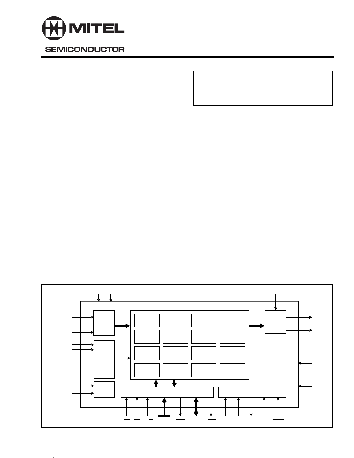
requirements. The MT9300 architecture contains 16
groups of two echo cancellers (ECA and ECB) which
can be configured to provide two channels of 64
milliseconds or one channel of 128 milliseconds
echo cancellation. This provides 32 channels of 64
milliseconds to 16 channels of 128 milliseconds echo
cancellation or any combination of the two
configurations. The MT9300 supports ITU-T G.165
and G.164 tone disable requirements.
Rin
Sin
MCLK
Fsel
C4i
F0i
V
DD
Serial
to
Parallel
PLL
Timing
Unit
V
SS
Echo Canceller Pool
Group 0
ECA/ECB
Group 4
ECA/ECB
Group 8
ECA/ECB
Group 12
ECA/ECB
DS CS R/W A10-A0 DTA D7-D0
Group 1
ECA/ECB
Group 5
ECA/ECB
Group 9
ECA/ECB
Group 13
ECA/ECB
Group 2
ECA/ECB
Group 6
ECA/ECB
Group 10
ECA/ECB
Group 14
ECA/ECB
IRQ
Group 3
ECA/ECB
Group 7
ECA/ECB
Group 11
ECA/ECB
Group 15
ECA/ECB
TDI TDO TCK TRSTTMS
Note:
Refer to Figure 3
for Echo Canceller
block diagram
Test PortMicroprocessor Interface
ODE
Parallel
to
Serial
Rout
Sout
IC0
RESET
Figure 1 - Functional Block Diagram
1
MT9300 Advance Information
ODE
Rout
IC0
V
SSVSS
IC0
IC0
IC0
IC0
DD
Sout
V
C4i
F0i
Rin
Sin
V
SS
NC
DD
V
NCNCNC
NC
V
SS
NCNCNC
V
NC
NCNCNCNCNC
DD
V
NCNCNCNCNC
SS
V
SS
IC0
IC0
NC
V
NC
NC
NC
NC
NC
NC
NC
NC
IC0
IC0
IC0
NC
NC
V
V
MCLK
V
V
Fsel
IC0
IC0
PLLVSS
PLLVDD
V
V
NC
NC
TMS
TDI
TDO
TCK
TRST
IC0
RESET
V
NC
DD
SS
SS
DD
DD
SS
SS
DD
121
123
125
127
129
131
133
135
137
139
141
143
145
147
149
151
153
155
157
159
103105107109
101 97115 113
160 Pin MQFP
171197252321193 295273113 151
936791
99
95111117119
33
858789
83 81
393735
79
77
75
73
71
69
65
63
61
59
57
55
53
51
49
47
45
43
41
NC
V
NC
V
V
NC
NC
NC
NC
NC
NC
NC
NC
NC
NC
NC
NC
V
NC
NC
NC
IC0
V
IC0
A10
A9
A8
V
A7
A6
A5
A4
V
A3
A2
A1
A0
V
NC
NC
DD
SS
SS
DD
SS
DD
SS
DD
SS
W
R/
NC
DTA
CS
DS
IRQ
VDDNC
NCNCNC
NC
VSSV
NC
D0
VSSNC
D1
D2
VDDD3
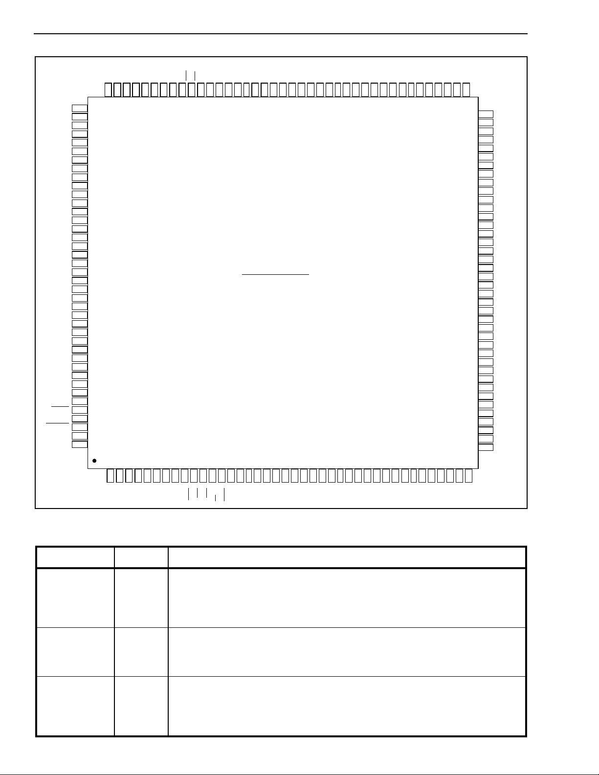
Figure 2 - Pin Connections
Pin Description
Pin # Name Description
1, 2, 17, 27, 37,
38, 48, 58, 76, 77,
81, 87, 98, 108,
118, 119, 138,
139, 148, 149
8, 22, 32, 43, 53,
63, 79, 93, 103,
113, 124, 141,
142, 159
57, 59, 114, 115,
116,117, 120,
121,122, 133,
134, 135, 144,
145, 157,
2
V
SS
V
DD
Ground.
Positive Power Supply. Nominally 3.3 volt.
IC0 Internal Connection. These pins must be connected to VSS for normal operation.
D4
D5
D6
NC
NC
NC
VSSD7
NC
NC
NC
VDDNC
NC
NC
VSSVSSNC

Advance Information MT9300
Pin Description (continued)
Pin # Name Description
3 to 7, 14 to 16,
28 to 31, 33 to 36,
39 to 42, 60 to 62,
64 to 75, 78, 80,
82 to 86, 88 to 92,
94 to 97, 99 to102,
104, 123,
125 to 132, 136,
137, 150,151,160
9 IRQ Interrupt Request (Open Drain Output). This output goes low when an interrupt
10 DS Data Strobe (Input). This active low input works in conjunction with CS to enable
11 CS Chip Select (Input). This active low input is used by a microprocessor to activate
12 R/W Read/Write (Input). This input controls the direction of the data bus lines (D7-D0)
13 DTA Data Transfer Acknowledgment (Open Drain Output). This active low output
NC No connection. These pins must be left open for normal operation.
occurs in any channel. IRQ returns high when all the interrupts have been read
from the Interrupt FIFO Register. A pull-up resistor (1K typical) is required at this
output.
the read and write operations.
the microprocessor port.
during a microprocessor access.
indicates that a data bus transfer is completed. A pull-up resistor (1K typical) is
required at this output.
18, 19, 20, 21,
23, 24, 25, 26
44, 45,46, 47,49,
50, 51,52,54, 55,
56
D0 - D3,
D4 - D7
Data Bus D0 - D7 (Bidirectional). These pins form the 8-bit bidirectional data bus
of the microprocessor port.
A0 - A10 Address A0 to A10 (Input). These inputs provide the A10 - A0 address lines to
the internal registers.
105 ODE Output Drive Enable (Input). This input pin is logically AND’d with the ODE bit-6
of the Main Control Register. When both ODE bit and ODE input pin are high, the
Rout and Sout ST-BUS outputs are enabled.
When the ODE bit is low or the ODE input pin is low, the Rout and Sout ST-BUS
outputs are high impedance.
106 Sout Send PCM Signal Output (Output). Port 1 TDM data output streams.
Sout pin outputs serial TDM data streams at 2.048 Mb/s with 32 channels per
stream.
107 Rout Receive PCM Signal Output (Output). Port 2 TDM data output streams. Rout pin
outputs serial TDM data streams at 2.048 Mb/s with 32 channels per stream.
109 Sin Send PCM Signal Input (Input). Port 2 TDM data input streams.
Sin pin receives serial TDM data streams at 2.048 Mb/s with 32 channels per
stream.
110 Rin Receive PCM Signal Input (Input). Port 1 TDM data input streams.
Rin pin receives serial TDM data streams at 2.048 Mb/s with 32 channels per
stream.
111 F0i Frame Pulse (Input). This input accepts and automatically identifies frame
synchronization signals formatted according to ST-BUS or GCI interface
specifications.
112 C4i Serial Clock (Input). 4.096 MHz serial clock for shifting data in/out on the serial
streams (Rin, Sin, Rout, Sout).
3

MT9300 Advance Information
Pin Description (continued)
Pin # Name Description
140 MCLK Master Clock (Input). Nominal 10MHz or 20MHz Master Clock input. May be
connected to an asynchronous (relative to frame signal) clock source.
143 Fsel Frequency select (Input). This input selects the Master Clock frequency
operation. When Fsel pin is low, nominal 19.2MHz Master Clock input must be
applied. When Fsel pin is high, nominal 9.6MHz Master Clock input must be
applied.
146 PLLV
147 PLLV
152 TMS Test Mode Select (3.3V Input). JTAG signal that controls the state transitions of
153 TDI T est Serial Data In (3.3V Input).JTAG serial test instructions and data are shifted
154 TDO Test Serial Data Out (Output). JTAG serial data is output on this pin on the falling
155 TCK Test Clock (3.3V Input). Provides the clock to the JTAG test logic.
156 TRST Test Reset (3.3V Input). Asynchronously initializes the JTAG TAP controller by
158 RESET Device Reset (Schmitt Trigger Input). An active low resets the device and puts
PLL Ground. Must be connected to V
SS
PLL Power Supply. Must be connected to V
DD
the TAP controller. This pin is pulled high by an internal pull-up when not driven.
in on this pin. This pin is pulled high by an internal pull-up when not driven.
edge of TCK. This pin is held in high impedance state when JTAG scan is not
enabled.
putting it in the Test-Logic-Reset state. This pin should be pulsed low on power-up
or held low , to ensure that the MT9300 is in the normal functional mode. This pin is
pulled by an internal pull-down when not driven.
the MT9300 into a low-power stand-by mode.
When the RESET pin is returned to logic high and a clock is applied to the
MCLK pin, the device will automatically execute initialization routines, which
preset all the Control and Status Registers to their default power-up values.
Device Overview
The MT9300 architecture contains 32 echo
cancellers divided into 16 groups. Each group has
two echo cancellers, Echo Canceller A and Echo
Canceller B. Each group can be configured in
Normal, Extended Delay or Back-to-Back
configurations. In Normal configuration, a group of
echo cancellers provides two channels of 64ms echo
cancellation, which run independently on different
channels. In Extended Delay configuration, a group
of echo cancellers achieves 128ms of echo
cancellation by cascading the two echo cancellers (A
& B). In Back-to-Back configuration, the two echo
cancellers from the same group are positioned to
cancel echo coming from both directions in a single
channel, providing full-duplex 64ms echo
cancellation.
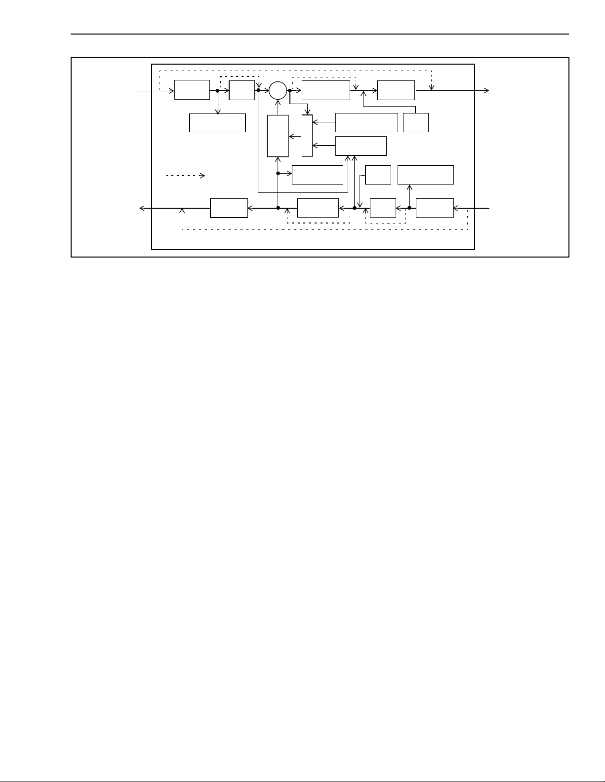
Each echo canceller contains the following main
elements (see Figure 3).
SS
DD
• Adaptive Filter for estimating the echo channel
• Subtractor for cancelling the echo
• Double-Talk detector for disabling the filter
adaptation during periods of double-talk
• Non-Linear Processor for suppression of
residual echo
• Disable Tone Detectors for detecting valid
disable tones at the input of receive and send
paths
• Narrow-Band Detector for preventing Adaptive
Filter divergence caused by narrow-band
signals
• Offset Null filters for removing the DC
component in PCM channels
• 12dB attenuator for signal attenuation
• Parallel controller interface compatible with
Motorola microcontrollers
• PCM encoder/decoder compatible with µ/ALaw ITU-T G.711 or Sign-Magnitude coding
4
Advance Information MT9300
Sin
(channel N)
ST-BUS
PORT2
Rout
(channel N)
µ/A-Law/
Linear
Disable Tone
Programmable
Bypass
Detector
Offset
Null
Linear/
µ/A-Law
Echo Canceller (N), where 0 ≤ N ≤ 31
+
-
Adaptive
Filter
Narrow-Band
Attenuator
Figure 3 - Echo Canceller Functional Block Diagram
Each echo canceller in the MT9300 has four
functional states:
and
Enable Adaptation
Mute,Bypass,Disable Adaptation
. These are explained in the
section entitled Echo Canceller Functional States.
Adaptive Filter
For each group of echo cancellers, the Adaptive
Filter is a 1024 tap FIR adaptive filter which is
divided into two sections. Each section contains 512
taps providing 64ms of echo estimation. In Normal
configuration, the first section is dedicated to
channel A and the second section to channel B. In
Extended Delay configuration, both sections are
cascaded to provide 128ms of echo estimation in
channel A. In Back-to Back configuration, the first
section is used in the receive direction and the
second section is used in the transmit direction for
the same channel.
Double-Talk Detector
Double-Talk is defined as those periods of time when
signal energy is present in both directions
simultaneously. When this happens, it is necessary
to disable the filter adaptation to prevent divergence
of the Adaptive Filter coefficients. Note that when
double-talk is detected, the adaptation process is
halted but the echo canceller continues to cancel
echo using the previous converged echo profile.
Non-Linear
Processor
Control
Detector
12dB
Microprocessor
Interface
Double-Talk
Detector
µ/A-Law
MuteR
Offset
Null
Linear/
MuteS
Disable Tone
Detector
µ/A-Law/
Linear
Sout
(channel N)
ST-BUS
PORT1
Rin
(channel N)
where DTDT is the Double-Talk Detection Threshold.
Lsin and Lrin are signal levels expressed in dBm0.
A different method is used when it is uncertain
whether Sin consists of a low level double-talk signal
or an echo return. During these periods, the
adaptation process is slowed down but it is not
halted. The convergence speed is shown by the
CONV bit in the Status Register.
In G.168 standard, the echo return loss is expected
to be at least 6dB. This implies that the Double-Talk
Detector Threshold (DTDT) should be set to 0.5
(-6dB). However, in order to get additional
guardband, the DTDT is set internally to 0.5625
(-5dB).
In some applications the return loss can be higher or
lower than 6dB. The MT9300 allows the user to
change the detection threshold to suit each
application’s need. This threshold can be set by
writing the desired threshold value into the DTDT
register.
The DTDT register is 16 bits wide. The register value
in hexadecimal can be calculated with the following
equation:
DTDT
= hex(DTDT
(hex)
(dec)
* 32768)
A double-talk condition exists whenever the relative
signal levels of Rin (Lrin) and Sin (Lsin) meet the
following condition:
Lsin > Lrin + 20log10(DTDT)
where 0 < DTDT
(dec)
< 1
Example: For DTDT = 0.5625 (-5dB), the
hexadecimal value becomes
hex(
0.5625 * 32768) = 4800h
5
MT9300 Advance Information
Non-Linear Processor (NLP)
After echo cancellation, there is always a small
amount of residual echo which may still be audible.
The MT9300 uses an NLP to remove residual echo
signals which have a level lower than the Adaptive
Suppression Threshold (TSUP in G.168). This
threshold depends upon the level of the Rin (Lrin)
reference signal as well as the programmed value of
the Non-Linear Processor Threshold register
(NLPTHR). TSUP can be calculated by the following
equation:
TSUP = Lrin + 20log10(NLPTHR)
where NLPTHR is the Non-Linear Processor
Threshold register value and Lrin is the relative
power level expressed in dBm0.
When the level of residual error signal falls below
TSUP, the NLP is activated further attenuating the
residual signal to less than -65dBm0. To prevent a
perceived decrease in background noise due to the
activation of the NLP, a spectrally-shaped comfort
noise, equivalent in power level to the background
noise, is injected. This keeps the perceived noise
level constant. Consequently, the user does not hear
the activation and de-activation of the NLP.
present for a minimum of one second with at least
one phase reversal, the Tone Detector will tr igger.
G.164 recommendation defines the disable tone as a
2100 Hz (±21Hz) sine wave with a power level
between 0 to -31dBm0. If the disable tone is present
for a minimum of 400 milliseconds, with or without
phase reversal, the Tone Detector will tr igger.
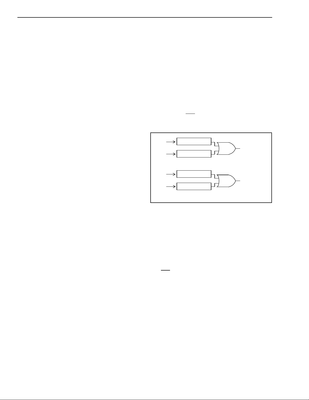
The MT9300 has two Tone Detectors per channels
(for a total of 64) in order to monitor the occurrence
of a valid disable tone on both Rin and Sin. Upon
detection of a disable tone, TD bit of the Status
Register will indicate logic high and an interrupt is
generated (i.e. IRQ pin low). Refer to Figure 4 and to
the Interrupts section.
Rin
Sin
Rin
Sin
Tone Detector
Tone Detector
Echo Canceller A
Tone Detector
Tone Detector
Echo Canceller B
ECA
Status reg
TD bit
ECB
Status reg
TD bit
The NLP processor can be disabled by setting the
NLPDis bit to “1” in Control Register 2.
The NLPTHR register is 16 bits wide. The register
value in hexadecimal can be calculated with the
following equation:
NLPTHR
where 0 < NLPTHR
= hex(NLPTHR
(hex)
< 1
(dec)
(dec)
* 32768)
The comfort noise injection can be disabled by
setting the INJDis bit to “1” in Control Register A1/
B1.
It should be noted that the NLPTHR is valid and the
comfort noise injection is active only when the NLP is
enabled.
Disable Tone Detector
G.165 recommendation defines the disable tone as
having the following characteristics: 2100 Hz
(±21Hz) sine wave, a power level between -6 to
-31dBm0, and a phase reversal of 180 degrees (±25
degrees) every 450ms (±25ms). If the disable tone is
Figure 4 - Disable Tone Detection
Once a Tone Detector has been triggered, there is
no longer a need for a valid disable tone (G.164 or
G.165) to maintain Tone Detector status (i.e. TD bit
high). The Tone Detector status will only release (i.e.
TD bit low) if the signals Rin and Sin fall below 30dBm0, in the frequency range of 390Hz to 700Hz,
and below -34dBm0, in the frequency range of
700Hz to 3400Hz, for at least 400ms. Whenever a
Tone Detector releases, an interrupt is generated
(i.e. IRQ pin low).
The selection between G.165 and G.164 tone
disable is controlled by the PHDis bit in Control
Register 2 on a per channel basis. When the PHDis
bit is set to 1, G.164 tone disable requirements are
selected.
In response to a valid disable tone, the echo
canceller must be switched from the Enable
Adaptation state to the Bypass state. This can be
done in two ways, automatically or externally. In
automatic mode, the Tone Detectors internally
control the switching between Enable Adaptation and
Bypass states. The automatic mode can be activated
by setting the AutoTD bit in Control Register 2 to
high. In external mode, an external controller is
needed to service the interrupts and poll the TD bits
6
Advance Information MT9300
in the Status Registers. Following the detection of a
disable tone (TD bit high) on a given channel, the
external controller must switch the echo canceller
from Enable Adaptation to Bypass state.
Narrow Band Signal Detector (NBSD)
Single or dual frequency tones (i.e. DTMF tones)
present in the receive input (Rin) of the echo
canceller for a prolonged period of time may cause
the Adaptive Filter to diverge. The Narrow Band
Signal Detector (NBSD) is designed to prevent this
divergence by detecting single or dual tones of
arbitrary frequency, phase, and amplitude. When
narrow band signals are detected, the adaptation
process is halted but the echo canceller continues to
cancel echo.
The NBSD can be disabled by setting the NBDis bit
to “1” in Control Register 2.
Offset Null Filter
Adaptive filters in general do not operate properly
when a DC offset is present at any inputs. To remove
the DC component, the MT9300 incorporates Offset
Null filters in both Rin and Sin inputs.
The offset null filters can be disabled by setting the
HPFDis bit to “1” in Control Register 2.
Device Configuration
The MT9300 architecture contains 32 echo
cancellers divided into 16 groups. Each group has
two echo cancellers which can be individually
controlled (Echo Canceller A and B). They can be set
in three distinct configurations: Normal, Back-to-
Back, and Extended Delay. See Figure 5.
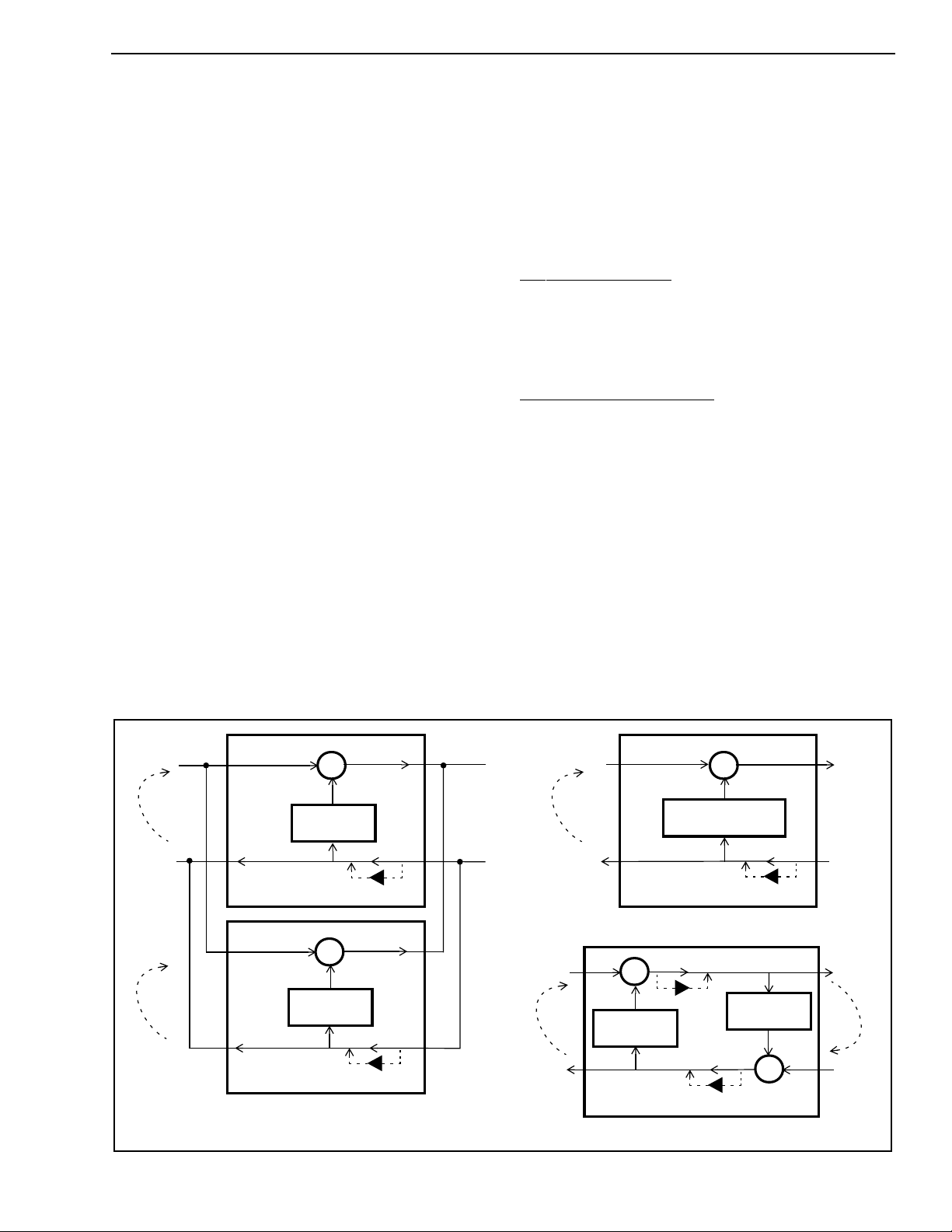
Normal Configuration
In Normal configuration, the two echo cancellers
(Echo Canceller A and B) are positioned in parallel,
as shown in Figure 5a, providing 64 milliseconds of
echo cancellation in two channels simultaneously.
Back-to-Back Configuration
In Back-to-Back configuration, the two echo
cancellers from the same group are positioned to
cancel echo coming from both directions in a single
channel providing full-duplex 64ms echo
cancellation. See Figure 5c. This configuration uses
only one timeslot on PORT1 and PORT2 and the
second timeslot normally associated with ECB
contains undefined data. Back-to-Back configuration
allows a no-glue interface for applications where
bidirectional echo cancellation is required.
Back-to-Back configuration is selected by writing “1”
into the BBM bit of both Control Register A1 and
Control Register B1 of a given group of echo
cancellers. Table 2 shows the 16 groups of 2
Sin
echo
path A
Rout
echo
path B
channel A
channel A
E.C.A
channel B
channel B
E.C.B
+
-
Adaptive
Filter (64ms)
Optional -12dB pad
+
-
Adaptive
Filter (64ms)
Optional -12dB pad
a) Normal Configuration (64ms)
Figure 5 - Device configuration
Sout
echo
path A
Rin
PORT1PORT2
Rout
Sin
channel A
channel A
E.C.A
+
-
Adaptive Filter
(128 ms)
Optional -12dB pad
Sout
Rin
PORT1PORT2
b) Extended Delay Configuration (128ms)
Sin
echo
path
Rout Rin
+
-
Optional -12dB pad
Adaptive
Filter (64ms)
E.C.A
Filter (64ms)
Optional -12dB pad
Adaptive
-
+
E.C.B
Sout
echo
path
PORT1PORT2
c) Back-to-Back Configuration (64ms)
7

MT9300 Advance Information
cancellers that can each be configured into Back-toBack.
Examples of Back-to-Back configuration include
positioning one group of echo cancellers between a
CODEC and a transmission device or between two
codecs for echo control on analog trunks.
Extended Delay configuration
In this configuration, the two echo cancellers from
the same group are internally cascaded into one 128
milliseconds echo canceller. See Figure 5b. This
configuration uses only one timeslot on PORT1 and
PORT2 and the second timeslot normally associated
with ECB contains undefined data.
Extended Delay configuration is selected by writing
“1” into the ExtDl bit in Echo Canceller A, Control
Register A1. For a given group, only Echo Canceller
A, Control Register A1, has the ExtDl bit. Control
Register B1, bit-0 must always be set to zero.
Table 2 shows the 16 groups of 2 cancellers that can
each be configured into 64ms or 128ms echo tail
capacity.
Echo Canceller Functional States
Canceller B must always be “0”. Refer to Figure 3
and to Control Register 2 for bit description.
Bypass
The Bypass state directly transfers PCM codes from
Rin to Rout and from Sin to Sout. When Bypass
state is selected, the Adaptive Filter coefficients
are reset to zero.
Disable Adaptation
When the Disable Adaptation state is selected, the
Adaptive Filter coefficients are frozen at their current
value. In this state, the adaptation process is halted
however the echo canceller continues to cancel
echo.
Enable Adaptation
In Enable Adaptation state, the Adaptive Filter
coefficients are continually updated. This allows
the echo canceller to model the echo return path
characteristics in order to cancel echo. This is the
normal operating state.
The echo canceller functions are selected in Control
Register A1/B1 and Control Register 2 through four
control bits: MuteS, MuteR, Bypass and AdaptDis.
Refer to the Registers Description for details.
Each echo canceller has four functional states:
Mute, Bypass, Disable Adaptation and Enable
Adaptation.
Mute
In Normal and in Extended Delay configurations,
writing a “1” into the MuteR bit replaces Rin with
quiet code which is applied to both the Adaptive
Filter and Rout. Writing a “1” into the MuteS bit
replaces the Sout PCM data with quiet code.
+Zero
(quiet code)
LINEAR
16 bits
2’s
complement
0000h 80h FFh D5h
SIGN/
MAGNITUDE
µ-Law
A-Law
CCITT (G.711)
µ-Law A-Law
Table 1 - Quiet PCM Code Assignment
In Back-to-Back configuration, writing a “1” into the
MuteR bit of Echo Canceller A, Control Register 2,
causes quiet code to be transmitted on Rout. Writing
a “1” into the MuteS bit of Echo Canceller A, Control
Register 2, causes quiet code to be transmitted on
Sout.
MT9300 Throughput Delay
The throughput delay of the MT9300 varies
according to the device configuration. For all device
configurations, Rin to Rout has a delay of two
frames and Sin to Sout has a delay of three frames.
In Bypass state, the Rin to Rout and Sin to Sout
paths have a delay of two frames.
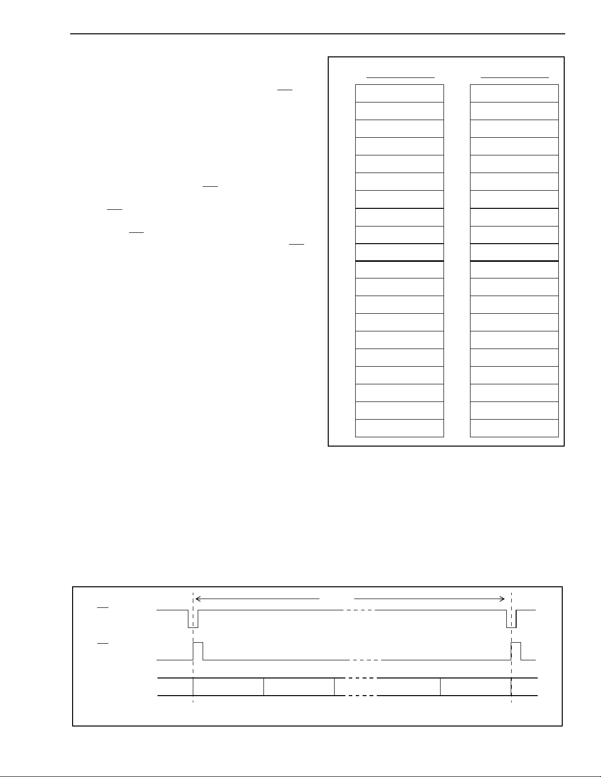
Serial PCM I/O channels
There are two sets of TDM I/O streams, each with
channels numbered from 0 to 31. One set of input
streams is for Receive (Rin) channels, and the other
set of input streams is for Send (Sin) channels.
Likewise, one set of output streams is for Rout pcm
channels, and the other set is for Sout channels. See
figure 6 for channel allocation.
The arrangement and connection of PCM channels
to each echo canceller is a 2 port I/O configuration
for each set of PCM Send and Receive channels, as
illustrated in Figure 3.
In Extended Delay and in Back -to -Back
configurations, MuteR and MuteS bits of Echo
8
Advance Information MT9300
Serial Data Interface Timing
The MT9300 provides ST-BUS and GCI interface
timing. The Serial Interface clock frequency, C4i, is
4.096 MHz. The input and output data rate of the STBus and GCI bus is 2.048 Mb/s.
The 8 KHz input frame pulse can be in either ST-BUS
or GCI format. The MT9300 automatically detects
the presence of an input frame pulse and identifies it
as either ST-BUS or GCI. In ST-BUS format, every
second falling edge of the C4i clock marks a bit
boundary, and the data is clocked in on the rising
edge of C4i, three quarters of the way into the bit cell
(See Figure 9). In GCI format, every second falling
edge of the C4i clock marks the bit boundary, and
data is clocked in on the second falling edge of C4i,
half the way into the bit cell (see Figure 10).
Memory Mapped Control and Status
registers
Internal memory and registers are memor y mapped
into the address space of the HOST interface. The
internal dual ported memory is mapped into
segments on a “per channel” basis to monitor and
control each individual echo canceller and
associated PCM channels. For example, in Normal
configuration, echo canceller #5 makes use of
Echo Canceller B from group 2. It occupies the
internal address space from 0A0h to 0BFh and
interfaces to PCM channel #5 on all serial PCM I/O
streams.
Base
Addr +
Echo Canceller A
Control Reg A1
00h
Control Reg 2
01h
Status Reg
02h
Reserved
03h
Flat Delay Reg
04h
Reserved
05h
Decay Step Size Reg
06h
Decay Step Number
07h
Reserved
08h
Reserved
0Ah
Rin Peak Detect Reg
0Ch
Sin Peak Detect Reg
0Eh
Error Peak Detect Reg
10h
Reserved
12h
DTDT Reg
14h
Reserved
16h
NLPTHR
18h
Step Size, MU
1Ah
Reserved
1Ch
Reserved
1Eh
Figure 7 - Memory Mapping of per channel
Control and Status Registers
Base
Addr +
Echo Canceller B
Control Reg B1
20h
Control Reg 2
21h
Status Reg
22h
Reserved
23h
Flat Delay Reg
24h
Reserved
25h
Decay Step Size Reg
26h
Decay Step Number
27h
Reserved
28h
Reserved
2Ah
Rin Peak Detect Reg
2Ch
Sin Peak Detect Reg
2Eh
Error Peak Detect Reg
30h
Reserved
32h
DTDT Reg
34h
Reserved
36h
NLPTHR
38h
Step Size, MU
3Ah
Reserved
3Ch
Reserved
3Eh
As illustrated in Figure 7, the “per channel” registers
provide independent control and status bits for each
echo canceller. Figure 8 shows the memory map of
the control/status register blocks for all echo
cancellers.
125 µsec
F0i
ST-Bus
F0i
GCI interface
Rin/Sin
Rout/Sout
Note: Refer to Figures 9 and 10 for timing details
Channel 1 Channel 30
Channel 31Channel 0
Figure 6 - ST-BUS and GCI Interface Channel Assignment for 2Mb/s Data Streams
9
 Loading...