ISO
2
-CMOS
MT9162
5 Volt Single Rail Codec
Advance Information
Features
• Single 5 volt supply
• Programmable µ−law/A-law Codec and filters
• Fully differential output driver
• SSI digital interface
• SSI speed control via external pins CSLO-CSL2
• Individual transmit and receive mute controls
• 0dB gain in receive path
• 6dB gain in transmit path
• Low power operation
• ITU-T G.714 compliant
Applications
• Cellular radio sets
• Local area communications stations
• Line cards
DS5178 ISSUE 4 August 1999
Ordering Information
MT9162AE 20 Pin Plastic DIP (300 mil)
MT9162AS 20 Pin SOIC
MT9162AN 20 Pin SSOP
-40°C to +85°C
Description
The MT9162 5V single rail Codec incorporates a
built-in Filter/Codec, transmit anti-alias filter, a
reference voltage and bias source. The device
supports both A-law and µ-law requirements.
The analog interface is capable of driving a 20k ohm
load.
The MT9162 is fabricated in Mitel's ISO2-CMOS
technology ensuring low power consumption and
high reliability.
VDD
VSS
VBias
VRef
Din
Dout
STB
CLOCKin
PCM
Serial
Interface
FILTER/CODEC GAIN
PWRST
Timing
IC
ENCODER
DECODER
A/µ CSL0 CSL1 CSL2 RXMute TXMute
6dB
0 dB
Control
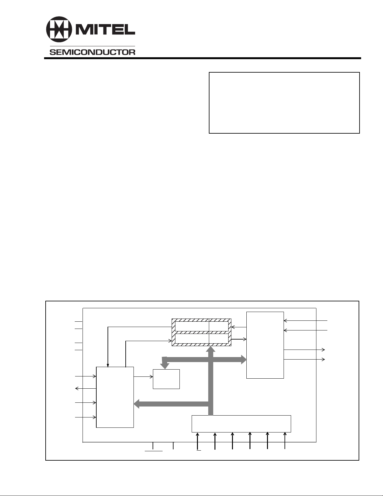
Figure 1 - Functional Block Diagram
Analog
Interface
AIN+
AIN-
AOUT +
AOUT -
7-161
MT9162 Advance Information
VBias
VRef
PWRST
A/µ
RXMUTE
TXMUTE
CSL0
CSL1
CSL2
1
2
3
4
IC
5
6
7
8
9
10
20
19
18
17
16
15
14
13
12
11
AIN+
AINVSS
AOUT +
AOUT VDD
CLOCKin
STB
Din
Dout
20 PIN PDIP/SOIC/SSOP
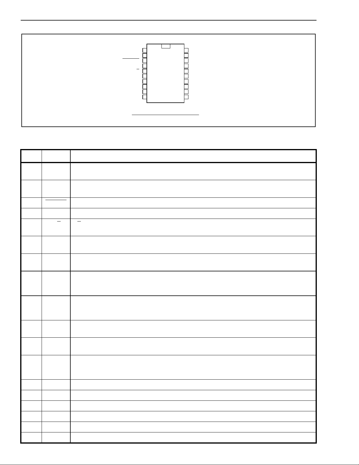
Figure 2 - Pin Connections
Pin Description
Pin # Name Description
1V
Bias
2V
3 PWRST Power-up Reset. Resets internal state of device via Schmitt Trigger input (active low).
4ICInternal Connection. Tie externally to VSS for normal operation.
Bias Voltage (Output). (VDD/2) volts is available at this pin for biasing external amplifiers.
Connect 0.1 µ F capacitor to VSS. Connect 1 µF capacitor to Vref.
Reference Voltage for Codec (Output). Nominally [(VDD/2)-1.9] volts. Used internally.
Ref
Connect 0.1 µ F capacitor to VSS. Connect 1 µF capacitor to VBias
5A/µ A/µ Law Selection. CMOS level compatable input pin governs the companding law used by
the device. A-law selected when pin tied to VDDor µ-law selected when pin tied to VSS.
6 RXMute Receive Mute. When 1, the transmit PCM is forced to negative zero code. When 0, normal
operation. CMOS level compatible.
7 TXMute Transmit Mute. When 1, the transmit PCM is forced to negative zero code. When 0, normal
operation. CMOS level compatible.
8
9
10
11 D
CSL0
CSL1
CSL2
out
Clock Speed Select. These pins are used to program the speed of the SSI mode as well as
the conversion rate between the externally supplied MCL clock and the 512 kHz clock required
by the filter/codec. Refer to Table 2 for details. CMOS level compatible.
Data Output. A tri-state digital output for 8-bit wide channel data being sent to the Layer 1
device. Data is shifted out via the pin concurrent with the rising edge of BCL during the timeslot
defined by STB.
12 D
Data Input. A digital input for 8-bit wide data from the layer 1 device. Data is sampled on the
in
falling edge of BCL during the timeslot defined by STB. CMOS level compatible.
13 STB Data Str obe. This input determines the 8-bit timeslot used by the device f or both transmit and
receive data. This active high signal has a repetition rate of 8 kHz. CMOS level compatible.
14 CLOCKin Clock (Input). The clock provided to this input pin is used by the internal device functions.
Connect bit clock to this pin when it is 512 kHz or greater . Connect a 4096 kHz cloc k to this pin
when the bit clock is 128 kHz or 256 kHz. CMOS level compatible.
15 V
Positive Power Supply. Nominally 5 volts.
DD
16 AOUT- Inverting Analog Output. (balanced).
17 AOUT+ Non-Inverting Analog Output. (balanced).
18 V
Ground. Nominally 0 volts.
SS
19 Ain- Inverting Analog Input. No external anti-aliasing is required.
20 Ain+ Non-Inverting Analog Input. Non-inverting input. No external anti-aliasing is required.
7-162
Advance Information MT9162
Overview
The 5V single rail Codec features complete Analog/
Digital and Digital/Analog conversion of audio
signals (Filter/Codec) and an analog interface to a
standard analog transmitter and receiver (Analog
Interface). The receiver amplifier is capable of
driving a 20k ohm load.
Functional Description
Filter/Codec
The Filter/Codec block implements conversion of the
analog 0-3.3 kHz speech signals to/from the digital
domain compatible with 64 kb/s PCM B-Channels.
Selection of companding curves and digital code
assignment are programmable. These are ITU-T
G.711 A-law or µ-Law, with true-sign/Alternate Digit
Inversion.
The Filter/Codec block also implements a transmit
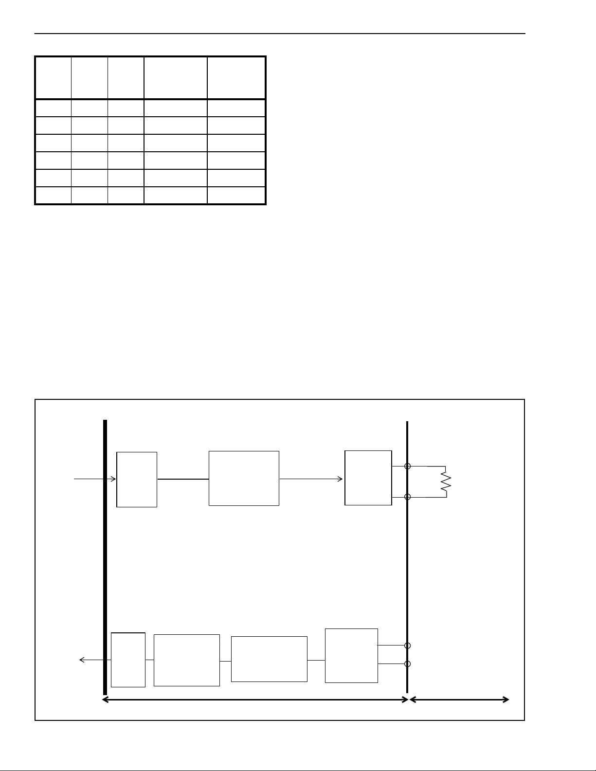
audio path gain in the analog domain. Figure 3
depicts the nominal half-channel for the MT9162.
The internal architecture is fully differential to provide
the best possible noise rejection as well as to allow a
wide dynamic range from a single 5 volt supply
design. This fully differential architecture is
continued into the analog interface section to provide
full chip realization of these capabilities for the
external functions.
A reference voltage (V
requirements of the Codec section, and a bias
voltage (V
), for biasing the internal analog
Bias
sections, are both generated on-chip. V
brought to an external pin so that it may be used for
biasing external gain setting amplifiers. A 0.1µF
capacitor must be connected from V
ground at all times. Likewise, although V
be used internally, a 0.1µF capacitor from the V
pin to ground is required at all times. The analog
ground reference point for these two capacitors must
be physically the same point. To facilitate this the
V
Ref
and V
pins are situated on adjacent pins.
Bias
The transmit filter is designed to meet ITU-T G.714
specifications. An anti-aliasing filter is included. This
is a second order lowpass implementation with a
corner frequency at 25 kHz.
), for the conversion
Ref
is also
Bias
to analog
Bias
may only
Ref
Ref
Companding law selection for the Filter/Codec is
provided by the A/
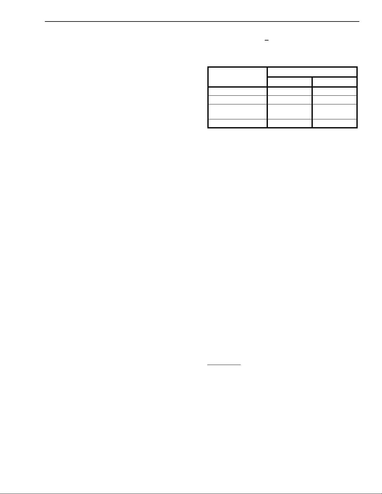
µ companding control pin. Table
1 illustrates these choices.
ITU-T (G.711)
Code
µ -Law A-Law
+ Full Scale 1000 0000 1010 1010
+ Zero 1111 1111 1101 0101
-Zero
(quiet code)
- Full Scale 0000 0000 0010 1010
0111 1111 0101 0101
Table 1: Law Selection
Analog Interfaces
Standard interfaces are provided by the MT9162.
These are:
• The analog inputs (transmitter), pins AIN+/AIN-.
The maximum peak to peak input is 3.667Vpp
µ−law and across AIN+/AIN- 3.8Vpp A-law.
• The analog outputs (receiver), pins AOUT+/
AOUT-.This internally compensated fully
differential output driver is capable of driving a
load of 20k ohms.
PCM Serial Interface
A serial link is required to transport data between the
MT9162 and an external digital transmission device.
The MT9162 utilizes the strobed data interface found
on many standard Codec devices. This interface is
commonly referred to as Simple Serial Interface
(SSI).
The required mode of operation is selected via the
CSL2-0 control pins. See Table 2 for selections
based in CSL2-0 pin settings.
Quiet Code
The PCM serial port can be made to send quiet code
to the decoder and receive filter path by setting the
RxMute pin high. Likewise, the PCM serial port will
send quiet code in the transmit path when the
The receive filter is designed to meet ITU-T G.714
specifications. Filter response is peaked to
compensate for the sinx/x attenuation caused by the
8 kHz sampling rate.
7-163
MT9162 Advance Information
The timing requirements for SSI are shown in
External
CSL2CSL1CSL
1 0 0 128 4096
1 0 1 256 4096
0 0 0 512 512
0 0 1 1536 1536
0 1 0 2048 2048
0 1 1 4096 4096
Clock Bit
0
Rate (kHz)
CLOCKin
(kHz)
Table 2: Bit Clock Rate Selection
TxMute pin is high. When either of these pins are low
their respective paths function normally. The -Zero
entry of Table 1 is used for the quiet code definition.
SSI Mode
Figures 5 & 6.
In SSI mode the MT9162 supports only B-Channel
operation. Hence, in SSI mode transmit and receive
B-Channel data are always in the channel defined by
the STB input.
The data strobe input STB determines the 8-bit
timeslot used by the device for both transmit and
receive data. This is an active high signal with an 8
kHz repetition rate.
SSI operation is separated into two categories based
upon the data rate of the available bit clock. If the bit
clock is 512 kHz or greater then it is used directly by
the internal MT9162 functions allowing synchronous
operation. If the available bit clock is 128 kHz or 256
kHz, then a 4096 kHz master clock is required to
derive clocks for the internal MT9162 functions.
The SSI BUS consists of input and output serial data
streams named Din and Dout respectively, a Clock
input signal (CLOCKin), and a framing strobe input
(STB). A 4.096 MHz master clock is also required for
SSI operation if the bit clock is less than 512 kHz.
Serial Port
PCM
D
in
Decoder
2.05 dB
Filter/Codec and Analog Interface
Receive
Filter Gain
0 dB
Applications where Bit Clock (BCL) is below 512 kHz
are designated as asynchronous. The MT9162 will
re-align its internal clocks to allow operation when
the external master and bit clocks are asynchronous.
Control pins CSL2, CSL1 and CSL0 are used to
program the bit rates.
-2.05 dB
Receiver
Driver
Aout +
Aout-
20kΩ
7-164
PCM
D
out
Encoder
-2.05 dB
Transmit Filter
Transmit Filter
Gain
Gain
0dB
0 to +7 dB
Transmit Gain
-0.37 dB
Transmit
Gain
8.42 dB
AIN+
AIN-
Analog
Input
(1 dB steps)
Internal To Device
External To Device
Figure 3 - Audio Gain Partitioning
Advance Information MT9162
For synchronous operation, data is sampled from
Din, on the falling edge of BCL during the time slot
defined by the STB input. Data is made available, on
Dout, on the rising edge of BCL during the time slot
defined by the STB input. Dout is tri-stated at all
times when STB is not true. If STB is valid, then quiet
code will be transmitted on Dout during the valid
strobe period. There is no frame delay through the
PCM serial circuit for synchronous operation.
For asynchronous operation Dout and Din are as
defined for synchronous operation except that the
allowed output jitter on Dout is larger. This is due to
the resynchronization circuitry activity and will not
affect operation since the bit cell period at 128 kb/s
and 256 kb/s is relatively large. There is a one frame
delay through the PCM serial circuit for
asynchronous operation. Refer to the specifications
of Figures 5 & 6 for both synchronous and
asynchronous SSI timing.
PWRST
While the MT9162 is held in PWRST no device
control or functionality is possible.
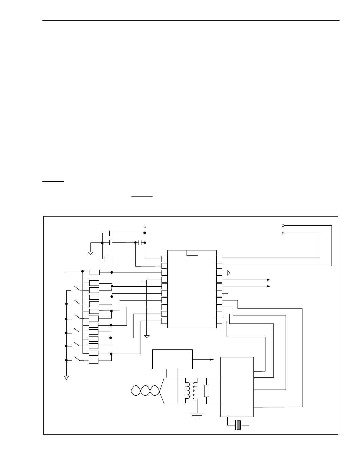
Applications
Figure 4 shows the MT9162 in a line card
application.
+5V
0.1 µF
0.1 µF
100k
100k
1k
100k
1k
100k
1k
CS0
100k
1k
CS1
100k
1k
CS2
100k
1k
From Digital
Phone
VBias
1 µF
A/µ
RxMUTE
TxMUTE
Twisted Pair
Typical External Gain
()
1
2
3
4
5
6
7
8
9
10
DC to DC
Converter
AV= 5-10
MT9162
20
19
18
17
16
15
14
13
12
11
+5V
Lin
Z
Lout
T
Input from Subscriber
Line Interface
+5V
Din
MT8972
DNIC
Dout
Frame Pulse
Clock
Out to Subscriber Line
Interface
Figure 4 - Line Card Application
7-165

MT9162 Advance Information
Absolute Maximum Ratings
†
Parameter Symbol Min Max Units
1 Supply Voltage VDD - V
2 Voltage on any I/O pin VI/V
3 Current on any I/O pin (transducers excluded) II/I
4 Storage Temperature T
5 Power Dissipation (package) P
†
Exceeding these values may cause permanent damage. Functional operation under these conditions is not implied.
Recommended Operating Conditions - Voltages are with respect to V
SS
O
O
S
D
SS
- 0.3 7 V
VSS - 0.3 VDD + 0.3 V
- 65 + 150 °C
unless otherwise stated
Characteristics Sym Min Typ Max Units Test Conditions
1 Supply Voltage V
2 CMOS Input Voltage (high) V
3 CMOS Input Voltage (low) V
4 Operating Temperature T
IHC
ILC
4.75 5 5.25 V
DD
4.5 V
V
SS
- 40 + 85 °C
A
DD
0.5 V
V
± 20 mA
750 mW
Power Characteristics
Characteristics Sym Min Typ Max Units Test Conditions
1 Static Supply Current (clock
disabled)
2 Dynamic Supply Current:
Total all functions enabled I
Note 1: Power delivered to the load is in addition to the bias current requirements.
I
DDC1
DDFT
420µA Outputs unloaded, Input
7.0 10 mA See Note 1
signals static, not loaded
7-166
 Loading...