MITEL MT9125AP, MT9125AE Datasheet

CMOS
MT9125
Dual ADPCM Transcoder
Preliminary Information
Features
• Dual chann el fu ll duple x trans c oder
• 32 kbit/s an d 24 k bit/s AD PC M codi ng,
• compatib le to G. 721 & and G .723 (1988) an d
ANSI T1.303-1989
• Low power o perat ion, tot al 25mW ty pical
• Asynchronous 4.096 M Hz m aster clock
operation
• Transparent ADP CM bypa ss cap abili ty
• Serial interf ace for bot h PCM and ADPCM data
streams
• ST-BUS interface supported
• Pin s ele cte d µ -la w or A-l aw o pe ra tio n
• Pin sele ct ed CCITT or sign-magnitude PCM
coding
• Single 5 vol t pow er suppl y
• Optional reset value (CCITT Table 3/G.721)
capabilit y
Applications
• Pair gain
• Voice mail systems
• Wireless set base sta tions
ISSUE 3 August 1993
Ordering Information
MT9125AE 24 Pin Plastic D IP
MT9125AP 28 Pin PLC C
-40 to +85°C
Description
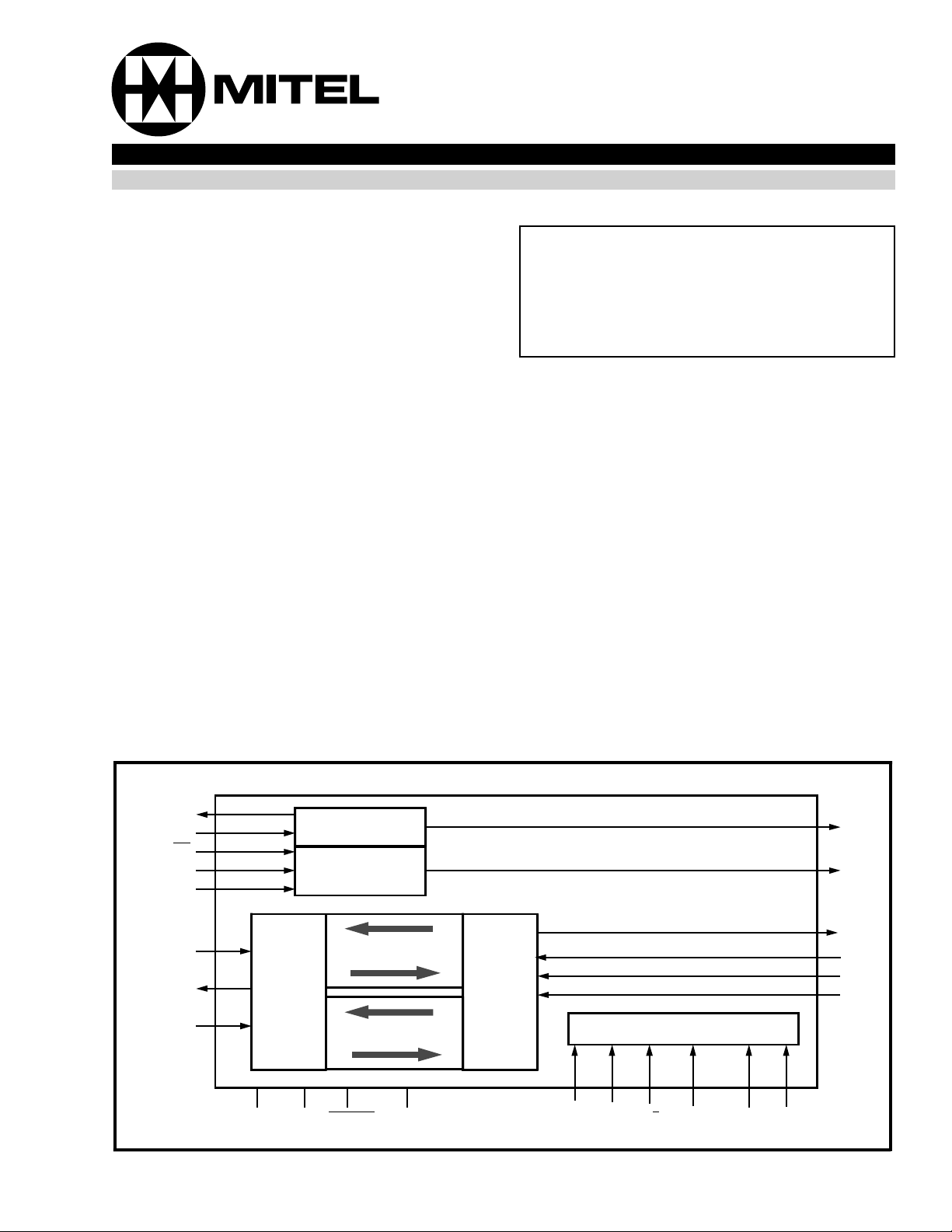
The Dual-channel ADPCM transcoder is a low
power, CMOS device capable of two encoder
functions and two decoder functions. Two 64 kbit/s
PCM channels are compressed into two 32 kbit/s
ADPCM channels, and two 32 kbit/s ADPCM
channels are expanded into two 64 kbit/s PCM
channels. The 32 kbit/s ADPCM transcoding
algorithm utilized conforms to CCITT Recommendation G.721 and ANSI T1.303-1989. The
device also supports a 24 kbit/s (three bit word)
algorithm (CCITT/G.723).
Switching, on-the-fly, between 32 kbit/s and 24
kbit/s, is possible by toggling the appropriate Mode
Select (MS1-MS4) control pins.
C2o
BCLK
F0i
MCLK
ENS
ADPCMi
ADPCMo
ENA
Timing
ST-BUS
Converter
ADPCM
I/O
VDD VSS PWRDN
Transcoder 1
Transcoder 2
PCM
I/O
Control Decode
IC MS1 MS2 A/µ FORMAT MS3 MS4
Figure 1 - Functional Block Diagram
EN1
EN2
DSTo
DSTi
ENB1
ENB2
8-17

MT9125 Preliminary Information
24 PIN PDIP
28 PIN PLCC
MCLK
DSTo
BCLK
ENB2
ENB1
DSTo
DSTi
BCLK
VSS
NC
ENB2
ENB1
F0i
C2o
DSTi
VSS
MS1
MS2
MS3
5
6
7
8
9
10
11
10
11
12
1
2
3
4
5
6
7
8
9
K
L
i
C
0
M
F
C
4
3
3
2
4
1
1
1
3
2
1
S
S
S
M
M
M
24
ENS
23
EN2
22
EN1
21
ADPCMo
20
ADPCMi
19
ENA
18
VDD
17
IC
16
PWRDN
15
FORMAT
14
A/µ
13
MS4
2
S
o
2
2
•
1
C
N
N
N
N
E
E
E
1
6
8
7
2
2
2
ADPCMo
25
ADPCMi
24
ENA
23
22
VDD
21
NC
20
IC
19
5
6
7
1
1
1
4
µ
C
/
S
N
A
M
PWRDN
8
1
T
A
M
R
O
F
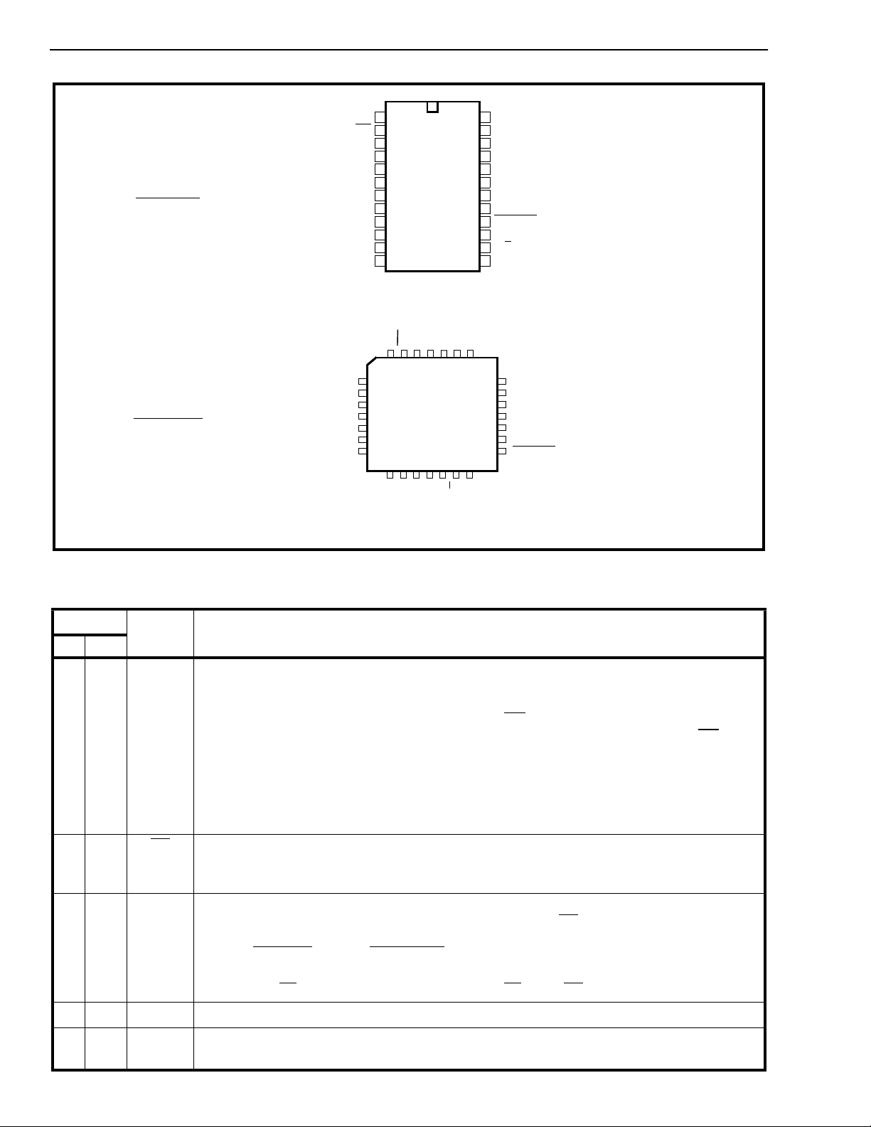
Figure 2 - Pin Connections
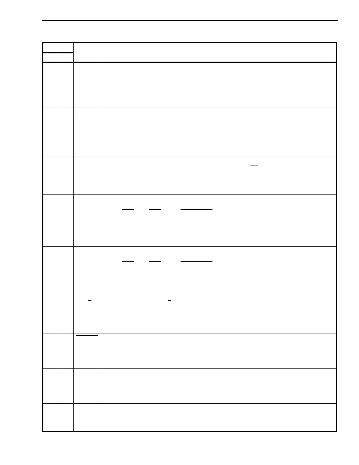
Pin Description
Pin #
DIP PLCC
1 2 MCLK Master Clock input. This 4.096 MHz clock is used as an internal master clock and must be
23 F0i
3 4 C2o 2.048MHz Clock output for ST-BUS applications. This clock is MCLK divided by 2 and
Name Description
provided during both ST-BUS and SSI modes of operation. This is a TTL level input.
In ST-BUS mode the MCLK input (also known as C4i
synchronous 4.096 MHz clock available from the layer 1 transceiver device. The C4i
input to MCLK, is used in this mode as both the internal master clock and for deriving the
C2o output clock and EN1/EN2 out put enable strobes.
In SSI mode a 4.096 MHz master clock must be derived from an external source. Th is
master clock may be asynchronous relative to the 8 kHz frame reference.
Frame alignment input pulse for ST-BUS interface operation. This input should be tied low
if ST-BUS operation is not required.
This is a TTL level input.
inverted. The C2o output activity state is governed by the F0i
F0i in pu t
V
SS
V
DD
Active F0i
strobe enabled and aligned to F0i due to C4i input at MCLK
C2o output
disabled (SSI mode automatically activated)
enabled
in ST-BUS terms) is derived from the
clock,
input pin condition.
4 5 DSTo S erial PCM octe t output stream. Refer to the serial timing diagram of Figure 12.
5 6 DSTi Serial PCM octet input data stream . Refer to the serial timing diagram of Figure 12.
This is a TTL level input.
8-18

Preliminary Information MT9125
Pin Description (continued)
Pin #
Name Description
DIP PLCC
6 7 BCLK Bit Clock input for both PCM and ADPCM ports; used in SSI mode only . The falling edge of
this clock is used to clock data in on DSTi and ADPCM i. The rising edge is used to clock
data out on DSTo and ADPCMo. Can be any rate between 128 kHz and 2.048 MHz. Refer
to the serial timing diagrams of Figures 12 and 13. When not used, this pin shoul d be tied
.
to V
SS
This is a TTL level input.
78 V
Power supply ground (0 volts).
SS
8 10 ENB2 Enable Strobe input for B2 channel PCM timing in SSI mode only. A valid 8-bit strobe must
be present at this input if there are no ST-BUS signals at F0i
detects a valid frame pulse at F0i
, PCM timing for the B2 ST-BUS channel is decoded
internally and the ENB2 input is ignored. When not used this pin should be tied to V
and MCLK. When the device
.
SS
This is a TTL level input.
9 11 ENB1 Enable Strobe input for B1 channel PCM timing in SSI mode only. A valid 8-bit strobe must
be present at this input if there are no ST-BUS signals at F0i
detects a valid frame pulse at F0i
, PCM timing for the B1 ST-BUS channel is decoded
internally and the ENB1 input is ignored. When not used this pin should be tied to V
and MCLK. When the device
.
SS
This is a TTL level input.
10, 1112, 13MS1,
MS2
Mode select control input pins 1 and 2 for the B1 channel according to the following:
MS2
MS1 B1 Channel
0 0 algorithm reset
0 1 ADPCM bypass mode (24 or 32 kbit/s)
1 0 24 kbit/s ADPCM mode
1 1 32 kbit/s ADPCM mode
These are TTL level inputs .
12,1314, 16MS3,
MS4
Mode select contro l input pins 3 and 4 for the B2 channel according to the following:
MS4
MS3 B2 Channel
0 0 algorithm reset
0 1 ADPCM bypass mode (24 or 32 kbit/s)
1 0 24 kbit/s ADPCM mode
1 1 32 kbit/s ADPCM mode
These are TTL level inputs .
14 17 A /µ
Law select input. Sel ects µ-Law when low, A-Law when high.
This is a TTL level input.
15 18 FORMA T Format select input. Selects CCITT PCM coding if high, or SIGN MAGNITUDE PCM if low.
This is a TTL level input.
16 19 PWRDN
Power Down input. Logic low on this pin forces the device to assume an internal power
down mode where all operation is halted. This mode mini mize s power consumption.
Outputs are tri- stated. This is a schmid t trig ger input .
17 20 IC Internal Connection. Tie to V
18 22 V
Positive power supply input, 5 volts ± 10%.
DD
for normal operation.
SS
19 23 ENA Enable S trobe input for both input and output ADPCM channels; used fo r SSI operation
only. Refer to Figure 3. When not used, tie to VSS.
This is a TTL level input.
20 24 ADPCMi Serial ADPCM word input data stream. Refer to the serial timing diagram of Fig. 13. This is
a TTL level input.
21 25 ADPC M o Serial ADPCM word output stream. Refer to the serial timing diagram of Fig.1 3.
8-19

MT9125 Preliminary Information
Pin Description (continued)
Pin #
DIP PLCC
22 26 EN1 Channe l 1 Output Enable strobe. This output is decoded from the ST-BUS C4i and F0i
23 27 EN2 Channe l 2 Output Enable strobe. This output is decoded from the ST-BUS C4i
24 28 ENS Enable S elect input for ST-BUS operation only. This control pin chang e s the ST-BUS
1, 9,
15,
21
Functional Description
The Dual-channel ADPCM Transcoder is a low
power, CMOS device capable of two encoder
functions and two decoder functions. Two 64 kbit/s
PCM channels (PCM octets) are compressed into
two 32 kbit/s ADPCM channels (ADPCM words), and
two 32 kbit/s ADPCM channels (ADPCM words) are
expanded into two 64 kbit/s PCM channels (PCM
octets). The ADPCM transcoding algorithm utilized
conforms to CCITT recommendation G.721 and
ANSI T1.303-1989. The device also supports a 24
kbit/s (three bit word) algorithm (CCITT/G.723).
Switching, on-the-fly, between 32 kbit/s and 24 kbit/s
is possible by toggling the appropriate Mode Select
(MS1 -MS4) cont ro l p in s .
The internal circuitry requires very little power to
operate; 25mW typically for dual channel operation.
A master clock frequency of 4.096 MHz is required
for the circuit to complete two encode channels and
two decode channels. Operation with an
asynchronous master clock, relative to the 8 kHz
reference, is allowed.
All optional functions of the device are pin selected,
no microprocessor is required. This allows a simple
interface with industry standard Codecs, Dual
Codecs, Digital Phone devices, and Layer 1
transceivers.
The PCM and ADPCM serial busses are a
Synchronous Serial Interface (SSI), allowing serial
clock rates from 128 kHz to 2.048 MHz. Additional
pins on the device allow an easy interface to an STBUS component. On chip channel counters provide
channel enable outputs, as well as a 2.048 MHz
Name Description
signals and its position, within the ST-BUS stream, may be controlled via the E NS pin.
Refer to the ST-BUS relative timing dia gram shown in Figure 4.
signals and its position, within the ST-BUS stream, may be controlled via the E NS pin.
Refer to the ST-BUS timing diagram shown in Figure 4.
channel position of EN1 and EN2 as well as the ADPCM channel position. Refer to the STBUS timing diagram shown in Figure 4. When not used this pin should be tied to V
is a TTL level input.
NC No Connect ion. Leave open cir cuit.
clock output, useful for driving the timing input pins
of standard CODEC devices.
Serial I/ O Ports (ADPCMi, ADPC Mo, EN A, EN B1,
ENB2, DSTi, DSTo, C2o, EN1, EN2, ENS, F0i
Serial I/O data transfer to the Dual ADPCM
Transcoder is provided through the PCM and the
ADPCM ports. Serial I/O port operation is similar for
both ST-BUS and SSI modes. The Dual ADPCM
Transcoder determines the mode of operation by
monitoring the signal applied to the F0i
valid ST-BUS Frame Pulse (244ns low going pulse)
is connected to the F0i
assume ST-BUS o p er a tion . If F 0i
to V
the transcoder will assume SSI operation. Pin
SS
functionality in each of these modes is described in
the following sub-sections.
ADPCM Port Operation (ADPCMi, ADPCMo, ENA)
The ADPCM port consists of ADPCMi, ADPCMo and
ENA. ADP CM port functionali ty is simi la r fo r both STBUS and SSI operation, the difference being in
where the BCLK signal is derived and in where the
ADPCM words are placed within the 8 kHz frame.
For SSI o perat ion (i .e., w hen F0i
to V
transferred over ADPCMi/ADPCMo at the bit clock
rate (BCLK) during the channel time defined by the
input strobe at ENA. Refer to Figure 3 and to Figure
13. Data is latched into the ADPCMi pin with the
falling edge of BCLK while output data is made
available at ADPCMo on the rising edge of BCLK.
) both channels of ADPCM code words are
SS
and F0i
DD
pin. When a
pin the transcoder will
is tied continuously
is tied continuously
. This
)
8-20

Preliminary Information MT9125
For ST-BUS operation (i.e., when a valid ST-BUS
frame pulse is applied to the F0i
input) the bit rate, at
2.048 MHz, is generated internally from the master
clock input at the MCLK pin. The BCLK and ENA
inputs are ignored. Data is latched into the ADPCMi
pin at the three-quarter bit position which occurs at
the second rising edge of MCLK (C4i
) within the bit
cell boundary. Output data, on ADPCMo, is made
available at the first falling edge of MCLK (C4i
) within
the bit cell boundary. Refer to Figure 13.
ADPCM word placement, within the ST-BUS frame,
is governed by the logic state applied at the ENS
input pin. Referring to Figure 4, when ENS = 0, the
ADPCM words are placed in channel 2 while when
ENS = 1 the ADPCM words are placed in channel 3.
Unlike the PCM octets the ADPCM words never
reside within the ST-BUS channel 0 or 1 timeslots.
PCM Port Operation (DSTi, DSTo, ENB1, ENB2)
The PCM port consists of DSTi, DSTo, ENB1 and
ENB2. PCM port functionality is almost identical for
both ST-BUS and SSI operation, the difference being
from where the BCLK signal is derived and whether
the enable strobes are generated internally or
sourced externally.
Both channels of PCM octets are transferred over
DSTi/DSTo at the bit clock rate during the channel
time defined by the input strobes at ENB1 and ENB2
or by internally generated timeslots.
For ST-BUS operation, (i.e., when a valid ST-BUS
frame pulse is applied to the F0i
input) the bi t r at e, at
2.048 MHz, is generated internally from the master
clock input at the MCLK pin. The BCLK and ENA
inputs are ignored. ST-BUS timeslot assignment is
also generated internally and can be programmed
into channels 0 and 1 or into channels 2 and 3 with
the ENS input pin. Refer to Figure 4. In this mode the
ENB1 and ENB2 inputs are ignored by the device.
The decoded channel timeslots (0 and 1 or 2 and 3)
are made available, along with the 2.048 MHz bit
clock, at EN1, EN2 and C2o for controlling CODEC
devices as shown in the Applications section (refer
to Figures 7 and 11). Data is latched into the DSTi
pin at the three-quarter bit position which occurs at
the second rising edge of MCLK (C4i
) within th e bit
cell boundary. Output data, on DSTo, is made
available at the first falling edge of MCLK (C4i
) within
the bit cell b oun d ary. Refer to Figu re 1 2 .
For SSI operation, (i.e., when F0i is tied continuously
to V
) the bit rate is set by the input clock presented
SS
at the BCLK pin. Data is transferred at the bit clock
rate (BCLK) during the B1 and B2 channels as
defined by input strobes ENB1 and ENB2,
respectively. Note that ENB1 and ENB2 are also
used as the framing inputs for internal operation of
ENB1
ENB2
DSTi/o
ENA
ADPCMi/o
8 bits
8 bits
B1 Channel B2 Channel
4 bits 4 bits
4 bits
B1 B2
Normally ENA is derived from the same strobes which drive the ENB1 or ENB2 inputs. However, as long as ENA
is eight cycles of BCLK length, it may be positioned anywhere within the 8 kHz frame.
4 bits
B1 B2
Figure 3 - SSI Mode Relative Timing
8-21
 Loading...