MITEL MT90863AG1, MT90863AL1 Datasheet
MT90863
3V Rate Conversion Digital Switch
Advance Information
Features
• 2,048 × 512 and 512 x 512 switching among
backplane and local streams
• Rate conversion between 2.048, 4.096 and
8.192Mb/s
• Optioal sub-rate switch configuration for
2.048 Mb/s streams
• Per-channel variable or constant throughput
delay
• Compatible to HMVIP and H.100 specifications
• Automatic frame offset delay measurement
• Per-stream frame delay offset programming
• Per-channel message mode
• Per-channel direction control
• Per-channel high impedance output control
• Non-multiplexed microprocessor interface
• Connection memory block programming
• 3.3V local I/O with 5V tolerant inputs and
TTL-compatible outputs
• IEEE-1149.1 (JTAG) Test Port
Applications
• Medium and large switching platforms
• CTI application
• Voice/data multiplexer
• Support ST-BUS, HMVIP and H.100 interfaces
DS5034 ISSUE 3 March 1999
Ordering Information
MT90863AL1 128 Pin MQFP
MT90863AG1 144 Pin BGA
-40 to +85 C
Description
The MT90863 Rate Conversion Switch provides
switching capacities of 2,048 × 512 channels
between backplane and local streams, and 512 x
512 channels for local streams. The connected serial
inputs and outputs may have 32, 64 and 128 64kb/s
channels per frame with data rates of 2.048Mb/s,
4.096Mb/s and 8.192Mb/s respectively.
The MT90863 also offers a sub-rate switching
configuration which allows 2-bit wide 16kb/s data
channels to be switched within the device.
The device has features (such as: message mode;
input and output offset delay; direction control; and,
high impedance output control) that are
programmable on per-stream or per-channel basis.
STio0/
FEi0
STio15/
FEi15
STio16/
FEi16
STio23/
FEi23
STio24
STio31
C16i
F0i
C4i/C8i
ODE
Backplane
Interface
S/P
&
P/S
Converter
Timing
Unit
F0o DS CS R/W A7-A0 DTA D15-D0
C4o
Multiple Buffer
(2,048 channels)
Internal
Registers
Microprocessor Interface
V
V
SS
DD
Data Memory
Local
Connection
Memory High/Low
(512 locations)
Backplane
Connection
Memory
(2,048 locations)
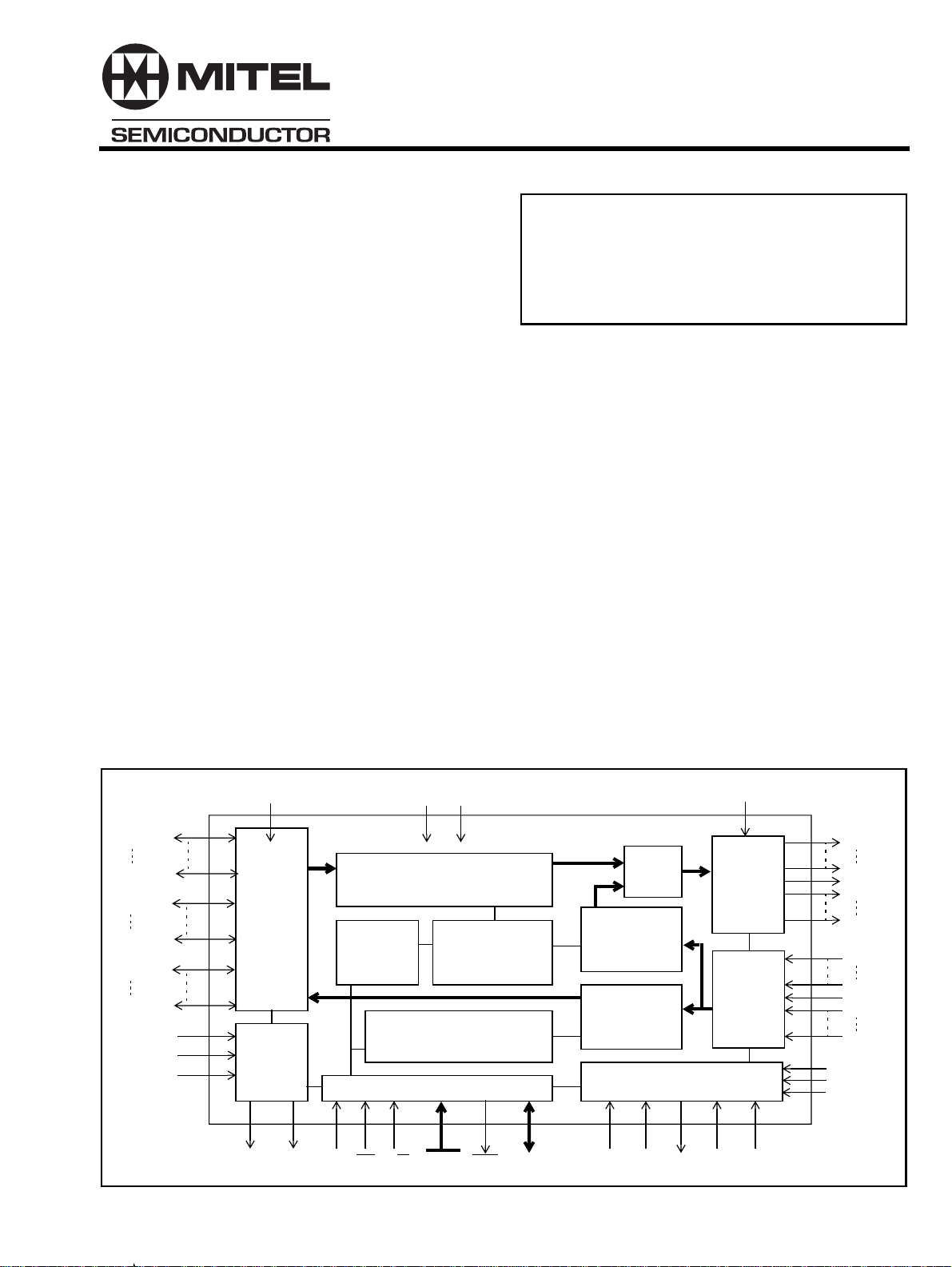
Figure 1 - Functional Block Diagram
Output
Mux
Multiple Buffer
Data Memory
(512 channels)
Multiple Buffer
Data Memory
(512 channels)
Test Port
TDI TDO
TMS
Interface
Converter
Interface
Converter
TCK
ODE
Local
P/S
Local
S/P
TRST
STo0
STo11
STo12
STo13
STo15
STi0
STi11
STi12
STi13
STi15
RESET
IC1
IC2
1
MT90863 Advance Information
VDD
STo0
STo1
STo2
STo3
STo4
STo5
STo6
STo7
VSS
VSS
C4o
F0o
VSS
F0i
C4i/C8i
VSS
C16i
VSS
STo14
ST015
STo12
STo13
STo10
STo11
STo8
STo9
VDD
ODE
VSS
STi14
STi15
VDD
STio0/FEi0
STio1/FEi1
STio2/FEi2
STio3/FEi3
STio4/FEi4
STio5/FEi5
STio6/FEi6
STio7/FEi7
VSS
VDD
STio8/FEi8
STio9/FEi9
STio10/FEi10
STio11/FEi11
STio12/FEi12
STio13/FEi13
STio14/FEi14
STio15/FEi15
VSS
VDD
STio16/FEi16
STio17/FEi17
STio18/FEi18
STio19/FEi19
STio20/FEi20
STio21/FEi21
STio22/FEi22
STio23/FEi23
VSS
VDD
STio24
97
99
101
103
105
107
109
111
113
115
117
119
121
123
125
127
79858789 7173757793 6791 69 6583 8195
128 Pin PQFP
171197252321193 295273113 151
63
STi12
STi11
STi13
61
STi10
STi9
59
STi8
STi7
57
STi6
STi5
55
STi4
STi3
53
STi2
STi1
51
STi0
VDD
49
VSS
DTA
47
D15
D14
45
D13
D12
43
D11
D10
41
D9
D8
39
VSS
D7
37
D6
D5
35
D4
D3
33
D2
STio25
STio26
STio27
STio28
STio29
STio30
VSS
STio31
TMS
TDI
TDO
TCK
IC1
TRST
IC2
VSS
RESET
A0
A4
A3
A2
A1
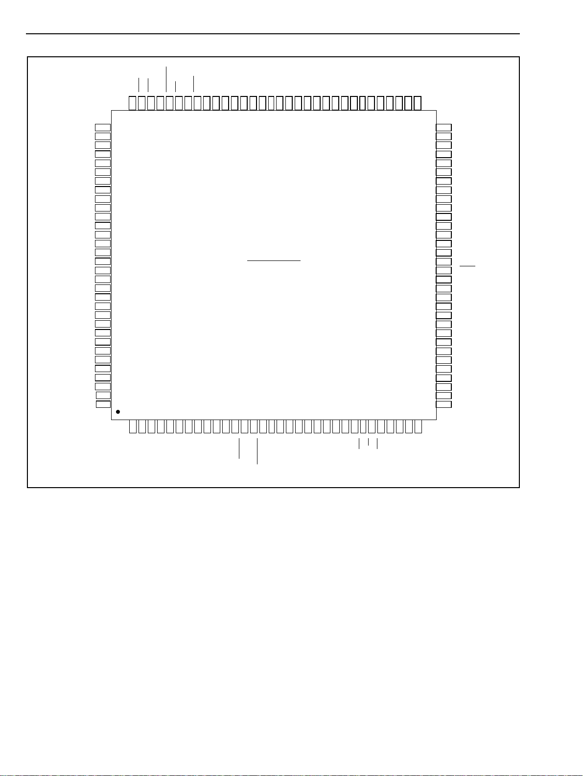
Figure 2 - MQFP Pin Connections
A5
A6
A7
DS
D1
D0
CS
R/W
VSS
VDD
2
Advance Information MT90863
1
A
B
C
D
E
F
G
H
J
K
L
M
N
12345678910111213
STio24
STio26
STio25
STio29
TMS
TDI
TDOTCK
TRST IC1RESET
A0
VSS
A1 A2 A3
A4A5 A6
A7
DS
R/WCS
D0D1D2D3D4
STio17
STio19
STio22
STio16
STio18
STio20
STio23
STio21
STio27STio28
STio30STio31
VSS
VSS
VDD
IC2
VSS
VDD
VSS
VDD
D5D6D7
VSS VSS
D8D9D10
TOP VIEW
D11
D12
D14D13
STio11
STio14STio15
STio10
STio13
STio12
D15
DTA STi0
STio9
VDD
STi1
STio6
STio8
STio5
STio7
VSSVSSVDD
VDD
VDDVSSVDDVSSVDDVSS VSS
VDD
VSS
VDD
VSS
VSS
VSSVDDVSSVDDVSSVDD VDD
STi6
STi8
STi7
STi4
STi2 STi3
STio3STio4
STio1STio2
C4o
STio0
C16iF0i
STo14
VSS
VDD
STo4 STo5STo6
VSS
VDD
STi12
STi15 ODE
STi13 STi14
STi10
STi5
STi9
F0o
C4i/C8i
STo15
STo13
STo11STo12
STo9STo10
STo7STo8
STo2STo3
STo0STo1
STi11
1 - A1 corner is identified by metallized markings.
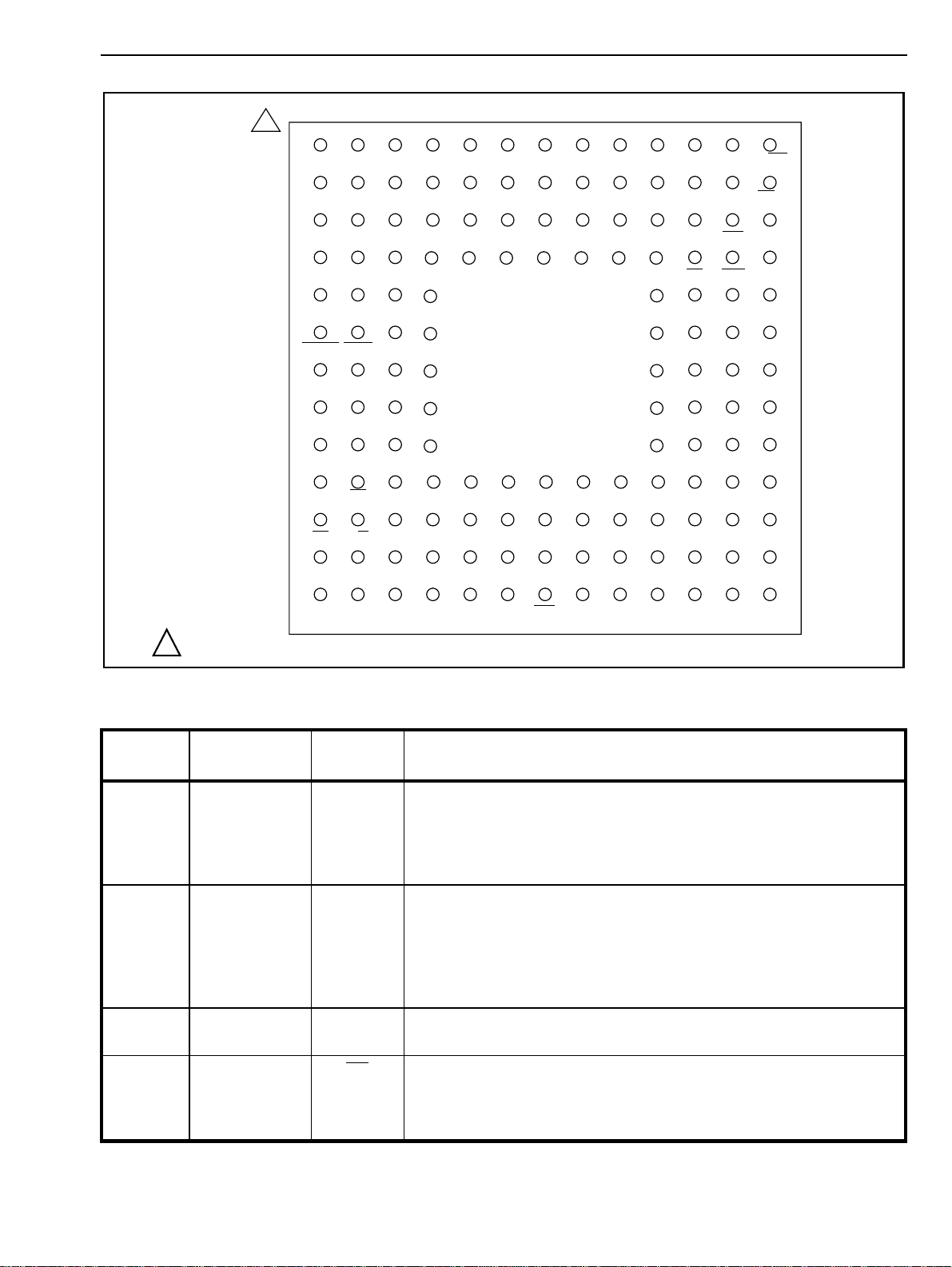
Figure 3 - BGA Pin Connections
Pin Description
128 MQFP
Pin#
30,50,67,
79,97,107,
117,127
8,17,29,39,
49,68,78,8
8,90,93,96,
106,
116,126
89 D12 C16i Master Clock (5V Tolerant Input): Serial clock for shifting data in/out
91 D11 F0i Master Frame Pulse (5V T olerant Input): In ST-BUS mode, this input
144 BGA
Pin#
C5,C9,D5,D7,
D9,E10,F4,G10
,G11,H4,
K3,K4,K6,K8
K10,K11,L8
C6,C10,D4,D6,
D8,D10,E3,E4,
F10,F11,G2,
G4,H10,J4,
J10,J11,K5
K7,K9,L3,L7
Name Description
V
DD
V
ss
+3.3 Volt Power Supply
Ground
on the serial streams. This pin accepts a 16.384 MHz clock.
accepts a 61ns wide negative frame pulse. In CT Bus mode, it accepts
a 122ns wide negative frame pulse. In HMVIP mode, it accepts a
244ns wide negative frame pulse.
3

MT90863 Advance Information
Pin Description (continued)
128 MQFP
Pin#
92 B13 C4i/C8i HMVIP/CT Bus Clock (5V Tolerant Input): When HMVIP mode is
94 A13 F0o Frame Pulse (5V Tolerant Output): A 244ns wide negative frame
95 C12 C4o C4 Clock (5V Tolerant Output): A 4.096MHz clock that is phase
98-105,
108-115
118-125 B6, A5, B5, A4,
144 BGA
Pin#
C11, B12, B11,
A12, A11, B10,
A10, B9, A9,
C8, B8, A8, C7,
B7, A7, A6,
B4, C4, A3, B3
Name Description
enabled, this pin accepts a 4.096MHz clock for HMVIP frame pulse
alignment. When CT Bus mode is enabled, it accepts a 8.192MHz
clock for CT frame pulse alignment.
pulse that is phase locked to the master frame pulse (F0i).
locked to the master clock (C16i).
STio0 - 15
FEi0 - 15
STio16 - 23
FEi16 - 23
Serial Input Streams 0 to 15 / Frame Evaluation Inputs 0 to 15 (5V
Tolerant I/O). In 2Mb/s and HMVIP modes, these pins accept serial
TDM data streams at 2.048 Mb/s with 32 channels per stream. In 4Mb/
s or 8Mb/s mode, these pins accept serial TDM data streams at 4.096
or 8.192 Mb/s with 64 or 128 channels per stream respectively. In
Frame Evaluation Mode (FEM), they are frame evaluation inputs.
Serial Input Streams 16 to 23 (5V Tolerant I/O). In 2Mb/s or 4Mb/s
mode, these pins accept serial TDM data streams at 2.048 or 4.096
Mb/s with 32 or 64 channels per stream respectively. In HMVIP mode,
these pins have a data rate of 8.192Mb/s with 128 channels per
stream. In Frame Evaluation Mode (FEM), they are frame evaluation
inputs.
128,
1-7
9 C1 TMS Test Mode Select (3.3V Input with internal pull-up): JTAG signal
10 D1 TDI Test Serial Data In (3.3V Input with internal pull-up): JTAG serial
11 E2 TDO T est Serial Data Out (3.3V Output):JTAG serial data is output on this
12 E1 TCK Test Clock (5V Tolerant Input): Provides the clock to the JTAG test
13 F2 TRST Test Reset (3.3 V Input with internal pull-up): Asynchronously
14 F3 IC1 Internal Connection 1 (3.3V Input with internal pull-down):
15 F1 RESET Device Reset (5V Tolerant Input): This input (active LOW) puts the
A2, B2, A1, C3,
C2, B1, D3, D2
STio24 - 31 Serial Input Streams 24 to 31 (5V Tolerant I/O). These pins are only
used for 2Mb/s or 4Mb/s mode. They accept serial TDM data streams
at 2.048 or 4.096 Mb/s with 32 or 64 channels per stream respectively.
that controls the state transitions of the TAP controller.
test instructions and data are shifted in on this pin.
pin on the falling edge of TCK. This pin is held in a high impedance
state when JTAG scan is not enabled.
logic.
initializes the JTAG TAP controller by putting it in the Test-Logic-Reset
state. This pin should be pulsed low on power-up, or held low
continuously, to ensure that the MT90863 is in the normal operation
mode.
Connect to VSS for normal operation.
MT90863 in its reset state. This clears the device’s internal counters
and registers. It also brings microport data bus STio0 - 31 and STo0 15 to a high impedance state.
16 G3 IC2 Internal Connection 2 (3.3V Input):
Connect to VSS for normal operation.
4

Advance Information MT90863
Pin Description (continued)
128 MQFP
Pin#
18-25 G1, H1, H2,
26 K2 DS Data Strobe (5V Tolerant Input): This active low input works in
27 L2 R/W Read/Write (5V Tolerant Input): This input controls the direction of
28 L1 CS Chip Select (5V Tolerant Input): Active low input used by a
31-38,
40-47
48 N7 DTA Data Transf er Acknowledgment (5V Tolerant Three-state Output):
51-54 N8, M8, N9,
144 BGA
Pin#
H3, J2, J1,J3,
K1
M1, N1, M2, N2,
M3, L4, N3, L5,
M4, N4, M5,
L6, M6, N5, N6,
M7,
N10
Name Description
A0 - A7 Address 0 - 7 (5V Tolerant Input): These lines provide the A0 to A7
address lines to the internal memories.
conjunction with CS to enable the read and write operations.
the data bus lines (D0-D15) during a microprocessor access.
microprocessor to activate the microprocessor port.
D0 - 7,
D8 - D15
STi0 - 3 Serial Input Streams 0 to 3 (5V Tolerant Inputs): In 2Mb/s or
Data Bus 0 -15 (5V T olerant I/O): These pins f orm the 16-bit data bus
of the microprocessor port.
This active low output indicates that a data bus tr ansfer is complete. A
pull-up resistor is required to hold a HIGH level when the pin is tristated.
Subrate Switching mode, these inputs accept data rates of 2.048 Mb/s
with 32 channels per stream. In 8Mb/s mode, these inputs accept data
rates of 8.192 Mb/s with 128 channels per stream.
55-62 M9, N11, L9,
M10, L10, N12,
M11, N13
63 L11 STi12 Serial Input Streams 12 (5V Tolerant Input): In 2Mb/s mode, this
64-66 M12, M13, L12 STi13 - 15 Serial Input Streams 13 to 15 (5V Tolerant Inputs): In 2Mb/s mode,
69 L13 ODE Output Drive Enable (5V Tolerant Input): This is the output enable
70-73 K13, K12, J13,
J12
74-77,
80-83
H11, H13, H12,
G13, G12, F13,
F12, E13
STi4 - 11 Serial Input Streams 4 to 11 (5V Tolerant Inputs): In 2Mb/s or Sub-
rate Switching mode, these inputs accept data rates of 2.048Mb/s
with 32 channels per stream.
input accepts data rate of 2.048Mb/s with 32 channels per stream
respectively. In Sub-rate Switching mode, this pin accepts 2.048Mb/s
with 128 channels per stream for Sub-rate switching application.
these inputs accept a data rate of 2.048Mb/s with 32 channels per
stream.
control for the STo0 to ST o15 serial outputs and STio0 to STio31 serial
bidirectional outputs.
STo0 - 3 Serial Output Streams 0 to 3 (5V T olerant Three-state Outputs): In
2Mb/s or Sub-rate Switching mode, these outputs have data rates of
2.048 Mb/s with 32 channels per stream respectively. In 8Mb/s mode,
these outputs have data rates of 8.192 Mb/s with 128 channels per
stream
STo4 - 7,
STo8 - 11
Serial Output Streams 4 to 11 (5V Tolerant Three-state Outputs):
In 2Mb/s or Sub-rate Switching mode, these outputs have data r ates of
2.048Mb/s with 32 channels per stream
5

MT90863 Advance Information
Pin Description (continued)
128 MQFP
Pin#
84 E12 STo12 Serial Output Streams 12 (5V Tolerant Three-state Output): In
85-87 D13, E11, C13 STo13 - 15 Serial Output Streams 13 to 15 (5V Tolerant Three-state Outputs):
Device Overview
The Rate conversion Switch (MT90863) can switch
up to 2,048 × 512 channels while also providing a
rate conversion capability. It is designed to switch 64
kb/s PCM or N X 64 kb/s data between the
backplane and local interfaces. When the device is in
the sub-rate switching mode, 2-bit wide 16 kb/s data
channels can be switched within the device. The
device maintains frame integrity in data applications
and minimum throughput delay for voice application
on a per channel basis.
144 BGA
Pin#
Name Description
2Mb/s mode, this output has data rate of 2.048Mb/s with 32 channels
per stream. In Sub-rate Switching mode, this pin has data rate of
2.048Mb/s with 128 channels per stream for Sub-rate switching
application.
In 2Mb/s mode, these outputs have a data rate of 2.048Mb/s with 32
channels per stream.
Frame Alignment Timing
The Device Mode Selection (DMS) register allows
users to select three different frame alignment timing
modes. In ST-BUS modes, the master clock (C16i) is
always at 16.384 MHz. The frame pulse (F0i) input
accepts a negative frame pulse at 8kHz. The frame
pulse goes low at the frame boundary for 61ns. The
frame pulse output F0o provides a 244ns wide
negative frame pulse and the C4o output provides a
4.094MHz clock. These two signals are used to
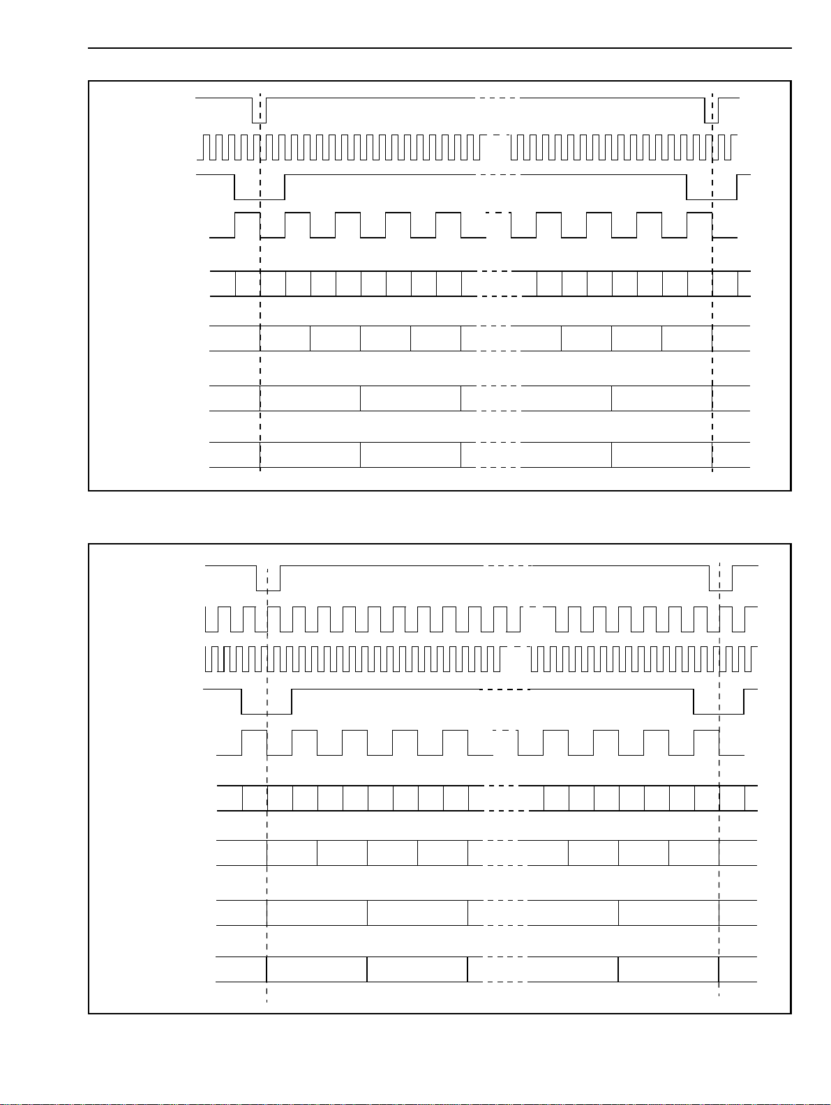
support local switching applications. See Figure 4 for
the ST-BUS timings.
The backplane interface can operate at 2.048, 4.096
or 8.192 Mb/s, arranged in 125µs wide frames that
contain 32, 64 or 128 channels, respectively. A builtin rate conversion circuit allows users to interface
between backplane interface and the local interface
which operates at 2.048 Mb/s or 8.192 Mb/s.
By using Mitel’s message mode capability, the
microprocessor can access input and output timeslots on a per channel basis. This feature is useful
for transferring control and status information for
external circuits or other ST-Bus devices.
The frame offset calibration function allows users to
measure the frame offset delay for streams STio0 to
STio23. The offset calibration is activated by a frame
evaluation bit in the frame evaluation register. The
evaluation result is stored in the frame evaluation
registers and can be used to programme the input
offset delay for individual streams using internal
frame input offset registers.
Functional Description
A functional Block Diagram of the MT90863 is shown
in Figure 1. One end of the MT90863 is used to
interface with backplane applications, such as
HMVIP or H.100 environments, while the other end
supports the local switching environments.
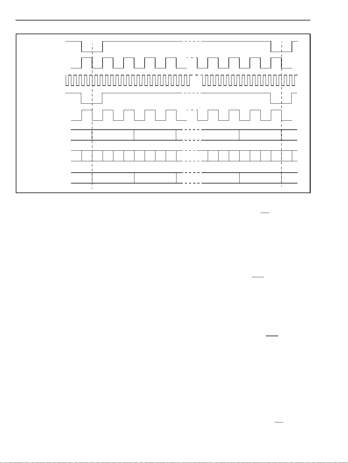
In CT Bus mode, the C4i/C8i pin accepts 8.192MHz
clock for the CT Bus frame pulse alignment. The F0i
is the CT bus frame pulse input. The CT frame pulse
goes low at the frame boundary for 122ns. See
Figure 5 for the CT Bus timing.
In HMVIP mode, the C4i/C8i pin accepts 4.096MHz
clock for the HMVIP frame pulse alignment. The F0i
is the HMVIP frame pulse input. The HMVIP frame
pulse goes low at the frame boundary for 244ns. See
Figure 6 for the HMVIP timing.
Table 1 describes the input timing requirements for
ST-BUS, CT Bus and HMVIP modes.
Switching Configuration
The device has four operation modes for the
backplane interface and three operation modes for
the local interface. These modes can be
programmed via the Device Mode Selection (DMS)
register. Mode selections between the backplane
and local interfaces are independent. See Table 2
and Table 3 for the selection of various operation
modes via the programming of the DMS register.
6
Advance Information MT90863
F0i
C16i
F0o
C4o
STio 0 - 15
STi/STo 0 - 3
(8Mb/s mode)
STio 0 - 31
(4Mb/s mode)
STio 0 - 31
STi/STo 0 - 15
(2Mb/s mode)
STi12/STo12
(Sub-rate
Switching)
F0i
(CT_FRAME)
C4i/C8i
(8.192MHz)
C16i
Channel 0
72345610
0
1
Channel 0
0
0
01 0
7564
Channel 0
76
Channel 0
Channel 127
Channel 63
Channel 31
1
Channel 127
Figure 4 - ST-BUS Timing for 2, 4 and 8 Mb/s Data Streams
2345610
12307
0
7
7
Bit 101
F0o
C4o
STio 0 - 15
STi/STo 0 - 3
(8Mb/s mode)
STio 0 - 31
(4Mb/s mode)
STio 0 - 31
STi/STo 0 - 15
(2Mb/s mode)
STi12/STo12
(Sub-rate
Switching)
Channel 0
72345610
0
1
Channel 0
0
0
01 0
7564
Channel 0
76
Channel 0
Channel 127
Channel 63
12307
Channel 31
1
Channel 127
Figure 5 - CT Bus Mode Timing for 2, 4 and 8 Mb/s Data Streams
2345610
0
7
7
Bit 101
7
MT90863 Advance Information
F0i
(HMVIP Frame)
C4i/C8i
(4.096MHz)
C16i
F0o
C4o
STio 0 - 15
STi/STo 0 - 15
(2Mb/s mode)
STio 16 - 23
(8Mb/s mode)
Channel 0
0
0
1
76
Channel 0
72345610
Channel 31
1
Channel 127
0
2345610
7
7
Channel 0
STi12/STo12
(Sub-rate
Switching)
01 0
Figure 6- HMVIP Mode Timing for 2 and 8 Mb/s Data Streams
Backplane Interface
The backplane interface can be programmed to
accept data streams of 2Mb/s, 4Mb/s or 8Mb/s.
When 2Mb/s mode is enabled, STio0 to STio31 have
a data rate of 2.048Mb/s. When 4Mb/s mode is
enabled, STio0 to STio31 have a data rate of
4.096Mb/s. When 8Mb/s mode is enabled, STio0 to
STio15 have a data rate of 8.192Mb/s. When HMVIP
mode is enabled, STio0 to STio15 have a data rate
of 2.048Mb/s and STio16 to STio23 have a data rate
of 8.192Mb/s.
Table 2 describes the data rates and mode selection
for the backplane interface.
Local Interface
Three operation modes, 2Mb/s, 8Mb/s and Sub-rate
Switching mode, can be selected for the local
interface. When 2Mb/s mode is selected, STi0 to
STi15 and STo0 to STo15 have a 2.048Mb/s data
rate. When 8Mb/s mode is selected, STi0 to STi3
and STo0 to STo3 have an 8.192Mb/s data rate.
When Sub-rate Switching mode is selected, STi0 to
STi11 and STo0 to STo11 have 2.048Mb/s data with
64kb/s data channels and STi12 and STo12 have a
2.048Mb/s data rate with 16kb/s data channels.
Table 3 describes the data rates and mode selection
for the local interface.
Input Frame Offset Selection
Input frame offset selection allows the channel
alignment of individual backplane input streams, that
Channel 127
Bit 101
operate at 8.192Mb/s (STio0-23), to be shifted
against the input frame pulse (F0i). This feature
compensates for the variable path delays caused by
serial backplanes of variable length. Such delays can
be occur in large centralized and distributed
switching systems.
Each backplane input stream can have its own delay
offset value by programming the input delay offset
registers (DOS0 to DOS5). Possible adjustment can
range up to +4 master clock (C16i) periods forward
with resolution of half master clock period. See Table
10 and Table 11, and Figure 9, for frame input delay
offset programming.
Output Advance Offset Selection
The MT90863 allows users to advance individual
backplane output streams which operate at 8.192Mb/
s (STio0-23) by half a master clock (C16i) cycle. This
feature is useful in compensating for variable output
delays caused by various output loading conditions.
The frame output offset registers (FOR0 & FOR1)
control the output offset delays for each backplane
output stream via the OFn bit programming. Table 12
and Figure 10 detail frame output offset
programming.
Serial Input Frame Alignment Evaluation
The MT90863 provides the frame evaluation inputs,
FEi0 to FEi23, to determine different data input
delays with respect to the frame pulse F0i. By using
the frame evaluation input select bits (FE0 to FE4) of
8

Advance Information MT90863
Timing Signals ST-BUS Mode CT Bus Mode HMVIP Mode
F0i Width 61ns 122ns 244ns
C4i/C8i Not Required 8.192MHz 4.096MHz
C16i 16.384MHz
F0o Width 244ns
C4o 4.096MHz
Table 1 - Timing Signals Requirements for Various Operation Modes
DMS Register Bits
Modes Backplane Interface Data Rate
BMS2 BMS1 BMS0
0 0 0 2Mb/s, ST-BUS Mode STio0 - 31 2.048 Mb/s
0 0 1 2Mb/s, CT Bus Mode STio0 - 31 2.048 Mb/s
0 1 0 4Mb/s, ST-BUS Mode STio0 - 31 4.096 Mb/s
0 1 1 4Mb/s, CT Bus Mode STio0 - 31 4.096 Mb/s
1 0 0 8Mb/s, ST-BUS Mode STio0 - 15 8.192 Mb/s
STio16 - 31 Not available
1 0 1 8Mb/s, CT Bus Mode STio0 - 15 8.192 Mb/s
STio16 - 31 Not available
1 1 0 HMVIP Mode STio0 - 15 2.048 Mb/s
STio16 - 23 8.192 Mb/s
STio24 - 31 Not available
Table 2 - . Mode Selection for Backplane interface
DMS Register Bits
Modes Local Interface Data Rate
LMS1 LMS0
0 0 2Mb/s Mode STi0 - 15 2.048 Mb/s
STo0 - 15 2.048 Mb/s
0 1 Sub-Rate
Switching
Mode
STi0 - 11 2.048 Mb/s
STi12 Sub-rate Switching Input Stream at 2.048 Mb/s
STi13 - 15 Not available
STo0 - 11 2.048 Mb/s
STo12 Sub-rate Switching Output Stream at 2.048Mb/s
STo13 - 15 Not available
1 0 8Mb/s Mode STi0 - 3 8.192 Mb/s
STi4 - 15 Not available
STo0 - 3 8.192 Mb/s
STo4 - 15 Not available
Table 3 - . Mode Selection for Local Interface
9

MT90863 Advance Information
the frame alignment register (FAR), users can select
one of the twenty-four frame evaluation inputs for the
frame alignment measurement.
A measurement cycle is started by setting the start
frame evaluation (SFE) bit low for at least one frame.
Then the evaluation starts when the SFE bit in the
Internal Mode Selection (IMS) register is changed
from low to high. One frame later, the complete
frame evaluation (CFE) bit of the frame alignment
register changes from low to high to signal that a
valid offset measurement is ready to be read from
bits 0 to 9 of the FAR register. The SFE bit must be
set to zero before a new measurement cycle is
started.
The falling edge of the frame measurement signal
(FEi) is evaluated against the falling edge of the
frame pulse (F0i). Table 8 and Figure 8 describe the
frame alignment register.
Memory Block Programming
The MT90863 has two connection memories: the
backplane connection memory and the local
connection memory. The local connection memory is
partitioned into high and low parts. The IMS register
provides users with the capability of initializing the
local connection memory low and the backplane
connection memory in two frames. Bit 11 to bit 13 of
every backplane connection memory location will be
programmed with the pattern stored in bit 7 to bit 9 of
the IMS register. Bit 12 to 15 of every local
connection memory low location will be programmed
with the pattern stored in bits 3 to 6 of the IMS
register.
The block programming mode is enabled by setting
the memory block program (MBP) bit of the control
register high. When the block programming enable
(BPE) bit of the IMS register is set to high, the block
programming data will be loaded into bits 11 to 13 of
every backplane connection memory and bits 12 to
15 of every local connection memory low. The other
connection memory bits are loaded with zeros. When
the memory block programming is complete, the
device resets the BPE bit to zero. See Figure 7 for
the connection memory contents when the device is
in block programming mode.
Delay Through the MT90863
delay to ensure minimum delay between input and
output data. In wideband data applications, select
constant throughput delay to maintain the frame
integrity of the information through the switch.
The delay through the device varies according to the
type of throughput delay selected in the L
BV/C bits of the local and backplane connection
memory as described in Table 16 and Table 19.
Variable Delay Mode (LV/C or BV/C bit = 0)
The delay in this mode is dependent only on the
combination of source and destination channels and
is independent of input and output streams.
Constant Delay Mode (LV/C bit or BV/C= 1)
In this mode a multiple data memory buffer is used
to maintain frame integrity in all switching
configurations.
V/C and
Microprocessor Interface
The MT90863 provides a parallel microprocessor
interface for non-multiplexed bus structures. This
interface is compatible with Motorola non-multiplexed
buses. The required microprocessor signals are the
16-bit data bus (D0-D15), 8-bit address bus (A0-A7)
and 4 control lines (CS, DS, R/W and DTA). See
Figure 16 for Motorola non-multiplexed bus timing.
The MT90863 microprocessor port provides access
to the internal registers, connection and data
memories. All locations provide read/write access
except for the Data Memory and the Data Read
Register which are read only.
Memory Mapping
The address bus on the microprocessor interface
selects the internal registers and memories of the
MT90863. If the A7 address input is low, then the
registers are addressed by A6 to A0 as shown in
Table 4.
If the A7 is high, the remaining address input lines
are used to select the serial input or output data
streams corresponding to the subsection of memory
positions. For data memory reads, the serial inputs
are selected. For connection memory writes, the
serial outputs are selected.
The switching of information from the input serial
streams to the output serial streams results in a
throughput delay. The device can be programmed to
perform time-slot interchange functions with different
throughput delay capabilities on a per-channel basis.
For voice applications, select variable throughput
10
The control, device mode selection and internal
mode selection registers control all the major
functions of the device. The device mode selection
register and internal mode selection register should
be programmed immediately after system power-up

Advance Information MT90863
1415
0 0
LBPD
3 2 1 0
0 0
2 1 0
1415
LBPD
1415
0
BBPDBBPDBBPD
LBPDLBPD
0
0 0
0
0000000000
Backplane Connection Memory (BCM)
0000000000
0
Local Connection Memory Low (LCML)
0
0000000000
Local Connection Memory High (LCMH)
765432108910111213
765432108910111213
765432108910111213
Figure 7 - Block Programming Data in the Connection Memories
A7
(Note 1)
A6 A5 A4 A3 A2 A1 A0 Location
0 0 0 0 0 0 0 0 Control Register, CR
0 0 0 0 0 0 0 1 Device Mode Selection Register, DMS
0 0 0 0 0 0 1 0 Internal Mode Selection Register, IMS
0 0 0 0 0 0 1 1 Frame Alignment Register, FAR
0 0 0 0 0 1 0 0 Input Offset Selection Register 0, DOS0
0 0 0 0 0 1 0 1 Input Offset Selection Register 1, DOS1
0 0 0 0 0 1 1 0 Input Offset Selection Register 2, DOS2
0 0 0 0 0 1 1 1 Input Offset Selection Register 3, DOS3
0 0 0 0 1 0 0 0 Input Offset Selection Register 4, DOS4
0 0 0 0 1 0 0 1 Input Offset Selection Register 5, DOS5
0 0 0 0 1 0 1 0 Frame Output Offset Register, FOR0
0 0 0 0 1 0 1 1 Frame Output Offset Register, FOR1
0 0 0 0 1 1 0 0 Address Buffer Register, ABR
0 0 0 0 1 1 0 1 Data Write Register, DWR
0 0 0 0 1 1 1 0 Data Read Register, DRR
1
1
1
1
1
1
1
.
1
1
Notes:
1. Bit A7 must be high for access to data and connection memory positions. Bit A7 must be low for access to registers.
2. Channels 0 to 31 are used when serial stream is at 2Mb/s.
3. Channels 0 to 127 are used when serial stream is at 8Mb/s
0
0
0
0
0
0
0
.
1
1
0
0
0
0
0
1
1
.
1
1
0
0
.
1
1
0
0
.
1
1
0
0
.
1
1
0
0
.
1
1
0
0
.
1
1
0
0
.
1
1
0
0
.
1
1
0
0
.
1
1
0
Ch 0
1
Ch 1
.
.
0
Ch 30
1
Ch 31 (Note 2)
0
Ch 32
1
Ch 33
.
.
0
Ch 126
1
Ch 127 (Note 3)
Table 4 - Address Memory Map
11
 Loading...