

Page 1
MT90840
Distributed Hyperchannel Switch
Preliminary Information
Features
• Time slot interchange function between eight
pairs of ST-BUS/GCI/MVIP streams (512
channels) and parallel data port
• Programmable data rates on the parallel port
(19.44, 16.384, or 6.480 Mbyte/s)
• Programmable data rates on the serial port
(2.048 Mbps, 4.096 Mbps or 8.192 Mbps)
• Supports star and point-to-point connections, and
unidirectional or bidirectional ring topologies for
distributed systems
• Input-to-output bypass function on the parallel
data port for use in add/drop applications
• Provides elastic buffer at parallel input port in the
receive direction
• Provides byte switching for up to 2430 channels
• Per-channel direction control on the serial port
side
• Per-channel message mode and high-impedance
control on both parallel and serial port sides
• 8-bit multiplexed microprocessor port compatible
with Intel and Motorola microcontrollers
• Guarantees frame integrity when switching nX64
wideband channels such as ISDN H0 channel
• Provides external control lines allowing fast
parallel interface to be shared with other devices
ISSUE 2 March 1997
Ordering Information
MT90840AL 100 Pin PQFP
MT90840AP 84 Pin PLCC
-40°C to 85°C
• Diagnostic alarm functions and clock
phase-status word for clock monitoring
• IEEE 1149 (JTAG) boundary scan port
Applications
• Bridging ST-BUS/MVIP buses to high speed
Time Division Multiplexed backplanes at
SONET rates (STS-1, STS-3)
• High speed isochronous backbones for
distributed PBX and LAN systems
• Switch platforms of up to 2430 channels with
guaranteed frame integrity for wideband
channels
• Serial bus control and monitoring
• Data multiplexing
• High speed communications interface
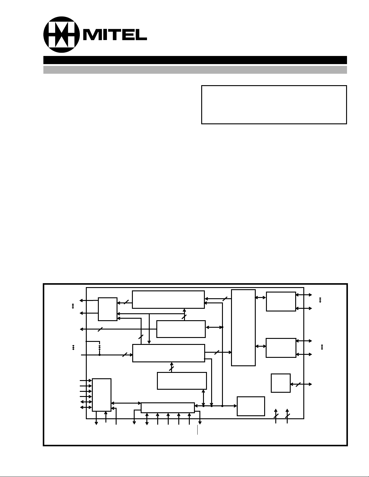
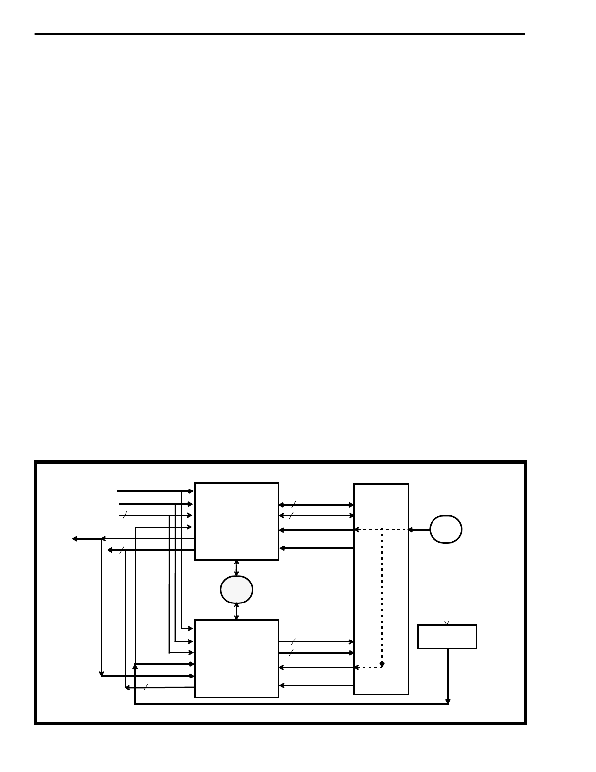
PDo0
PDo7
CTo0-3
PDi0
PDi7
PCKR
PCKT
RES
PPFRi
PPFTi/o
F0i/o
Output
Mux &
Drivers
4
Timing
Control
Unit
SPCKo
C4/8R1
C4/8R2
Multiple Pages of 512 Position
8
8
TX Path Data Memory
16
2430 Position
TX Path
Connection Memory
8
Multiple Pages of 2430-Byte
RX Path Data Memory
15
512 Position
RX Path
Connection Memory
CPU Interface
IRQ
AD0-7
DS/RD
AS/ALE
R/W\WR
CS
DTA
Figure 1 - Functional Block Diagram
Serial
8
to
Parallel
&
Parallel
to
Serial
8
Conver-
ters
Internal
Registers
Bidirectional
I/O
Driver
Bidirectional
I/O
Driver
JTAG
8
VDD
VSS
8
STi0
STi7
STo0
STo7
5
TEST
Pins
2-231
Page 2
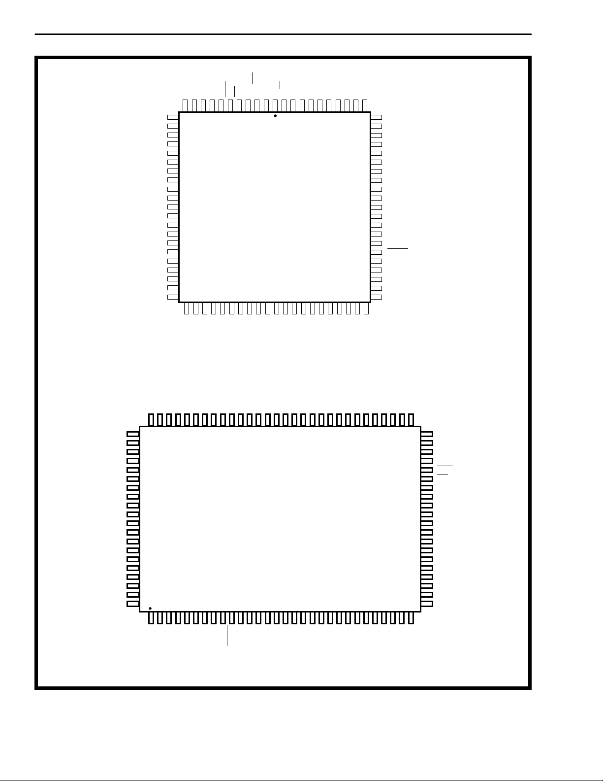
MT90840 Preliminary Information
RD
DS/
VDD
2
42
VSS
W
R/
84
44
AD7
AD6
82
46
AD5
AD4
80
48
AD3
AD2
78
50
AD1
AD0
74
76
72
70
68
66
64
62
60
58
56
54
52
VDD
VSS
STo0
STo1
STo2
STo3
STo4
STo5
STo6
STo7
SPCKo
VSS
VDD
TDO
TMS
TCK
TRST
TDI
PPFRi
PCKT
PCKR
VDD
VDD
STi0
STi1
STi2
STi3
STi4
STi5
STi6
STi7
C4/8R1
F0i/o
C4/8R2
VSS
VDD
NC
NC
CTo3
CTo2
CTo1
CTo0
VSS
12
14
16
18
20
22
24
26
28
30
32
VSS
NC
10
34
IC
RES
8
IRQ
DTA
6
CS
AS/ALE
4
84 PIN PLCC
36
38
40
PDo7
PDo6
PDo5
PDo4
PDo3
PDo2
PDo1
PDo0
PPFTi/o
VSS
VDD
PDi7
PDi6
PDi5
PDi4
PDi3
PDi2
PDi1
PDi0
VSS
82
84
86
88
90
92
94
96
98
100
NC
NC
NC
NC
VDD
NC
PDo6
PDo7
VSS
VDD
PDo4
PDo5
CTo1
CTo0
PDo0
PDo1
PDo2
PDo3
VSS
CTo3
VDD
CTo2
100 PIN PQFP
VSS
VDD
PPFTi/o
C4/8R2
C4/8R1
F0i/o
PDi7
STi7
PDi4
PDi5
PDi6
STi6
PDi2
PDi3
STi3
STi2
STi4
STi5
22 24 26 28 30
2018161412108642
PDi0
PDi1
STi0
STi1
VSS
VDD
VSS
NC
NC
NC
NC
525456586062646668707274767880
50
NC
IC
48
RES
IRQ
46
DTA
CS
44
AS/ALE
/RD
DS
42
VDD
VSS
40
R/W
AD7
38
AD6
AD5
36
AD4
AD3
34
AD2
AD1
32
AD0
NC
2-232
NCNCNC
NC
VDD
PCKR
PCKT
PPFRi
TDI
TCK
TRST
TMS
TDO
VSS
VDD
Figure 2 - Pin Connections
STo7
STo6
SPCKo
STo5
STo4
STo3
STo2
STo0
STo1
VSS
NCNCNC
VDD
NC
Page 3

Preliminary Information MT90840
Pin Description
Pin #
84 100
343DS/RD Data Strobe/Read (Input). In Motorola multiplexed-bus mode this pin is DS, an
4 44 AS/ALE Address Strobe / Address Latch Enable (Input ). Falling edge is used to sample
545 CS Chip Select (Input). Active low input enabling a microprocessor read or write of
646 DTA Data Acknowledgment (Active Low Output). Indicates that a data b us transf er is
7 47 IRQ Interrupt Request (Active High Output). Output indicates that the MT90840 has
Name Description
active high input which works with CS to enable read and write operation. In Intel/
National multiplexed-bus mode this pin is RD, an active low input which enables a
read-cycle and configures the data bus lines (AD0-AD7) as outputs.
address into the Address Latch circuit.
control or status registers.
complete. When the bus cycle ends, this pin drives HIGH and then tri-states,
allowing for faster bus cycles with a weaker pull-up resistor. A pull-up resistor is
required to hold a HIGH level when the pin is tri-stated. Note that CPU read/writes
from/to the Data and Connection memories occur on the serial or parallel port
clock edges, and DTA will not change state if the clock is halted.
detected an alarm condition. The indication of the specific condition can be read in
the ALS (Alarm Status) Register. The CPU should read ALS, identify the source f or
the interrupt and then rewrite the mask bits to re-enable the IRQ signal.
8 48 RES RESET (Schmitt Input). Asynchronous device reset. A logic-high signal should be
applied during power-up to bring the MT90840 internal circuitry to a defined state.
Serial and parallel TDM outputs (STo0-7, STi0-7, and PDo0-7) are held in
high-impedance state after reset until programmed otherwise. This input must be
held low during normal operation.
949 ICInternal Connection. The user must connect this pin to VSS. This pin must remain
low for the MT90840 to function normally, and to comply with IEEE 1149 (JTAG)
boundary scan requirements. This pin is pulled low internally when not driven.
10, 26,
27
13-20 57-64 STi0-STi7 Serial Inputs 0 to 7 (Bidirectional). Serial TDM data-streams at 2.048, 4.096 or
21 65 C4/8R1 Serial Clock Reference Input 1. When enabled by the C4/8R bit (high) in the TIM
1-4, 27-31 50-54 76-80
NC No Connection.
8.192 Mbps, with 32, 64 or 128 channels respectively per stream. For 2.048 and
4.096 Mbps applications, streams STi0-STi7 can be used, while for 8.192 Mbps,
only streams STi0-STi3 are used (512 channel limit). These eight bidirectional
lines can be programmed as inputs (default) or outputs on a per-channel basis.
Register, this input receives the 4.096 or 8.192 MHz serial port clock reference. If
the C4/8R bit is set low, or if the INTCLK bit is set high, this input is ignored by the
MT90840.
In Timing Mode 1 (TM1), or at 8.192 MHz, the C4/8 input is used directly to shift
data in and out of the serial port.
In Timing Mode 2 (TM2) at 4.096 MHz, the C4 input from an external clock source
(e.g. a PLL locked to an 8 kHz ref erence) is phase-corrected b y the MT90840, and
used to generate the serial port SPCKo and F0 outputs.
In Timing Modes 3 and 4 (TM3 and TM4) this input is not used.
For more details on the use of this signal, see the description of Timing Mode 1
and Timing Mode 2.
2-233
Page 4

MT90840 Preliminary Information
Pin Description (continued)
Pin #
84 100
22 66 F0i/o Serial Port Frame Synchronization (Bidirectional). This 8 kHz frame pulse
23 67 C4/8R2 C4/8R2 Serial Clock Reference Input 2. When enabled by the C4/8R bit (low) in
Name Description
signal indicates the TDM 125 µsec frame boundary on the serial data port. This
pin is compatible with both ST-BUS/MVIP and GCI formatted framing signals.
In TM1 this pin is an input, and the MT90840 senses the polarity of this frame
pulse and automatically adapts the serial data port timing to the applicable format
(ST-BUS or GCI).
In TM2 with SFDI =1 this signal is an input, and its expected format is determined
by the SPFP bit in the GPM Register.
In TM2 (with SFDI =0), and in TM3, this signal is an output, generated from the
internal timing and synchronized to the SPCKo output clock. The polarity of the F0
pulse is determined by the SPFP bit in the GPM Register.
In TM4 this pin is not used.
the TIM Register, this input receives the 4.096 or 8.192 MHz serial port clock
reference. If the C4/8R bit is set high, or if the INTCLK bit is set high, this input is
ignored by the MT90840. (See pin description for C4/8R1.)
28-31 70-73 CTo3-
CTo0
34-41 81-88 PDo7-PDo0Parallel Data Output Port 7 to 0 (Output). These eight outputs carry the parallel
42 89 PPFTi/o Parallel Port Framing, Transmit (Bidirectional). This signal delineates the start
45-52 92-99 PDi7-0 Parallel Data Input Port 7 to 0 (Input). These eight inputs carry the parallel port
55 6 PCKR Parallel Port Clock, Receive (Input). This is a 19.44, 16.384, or 6.48 MHz clock
56 7 PCKT Parallel Port Clock, Transmit (Input). This is a 19.44, 16.384, or 6.48 MHz clock
57 8 PPFRi Parallel Port Framing, Receive (Input). This 8 kHz frame pulse input determines
External Control Lines 3 to 0 (Output). Output signals generated from the
MT90840 Transmit Path Connection Memory (TPCM). The four serial CTo output
lines represent the contents of the four CT bits in the TPCM, and are clocked at the
parallel port rate (up to 19.44 MHz). See Per-Channel Functions section.
port data bytes in the transmit direction and operate at data rates up to 19.44
Mbyte/s.
of a new data frame at the PDo0-7 lines on the transmit parallel port. Normally an
output, when the PFDI bit in the TIM Register is set high PPFT becomes an input,
and is used to receive the frame reference from another MT90840. Used in all
timing modes except TM3.
data bytes in the receive direction and operate at data rates up to 19.44 Mbyte/s.
input. It might typically be provided by a high speed framer. PCKR clocks in data
on the receive parallel port (PDi7-0 and PPFRi). In Timing Modes 2, 3, and 4,
PCKR clocks both the transmit and receive parallel ports.
input. It might typically be provided by a high speed framer. In TM1 PCKT clocks
out the data on the transmit parallel port (PDo0-7, CTo0-3, and PPFTo). In TM2,
TM3, & TM4, this input is ignored.
the start of a new frame at the PDi0-7 lines of the receive parallel port. It might
typically be connected to the frame pulse output of a high speed framer. In TM3,
PPFRi is the frame sync reference for both the transmit and receive parallel ports.
58 9 TDI Test Data (Input). JTAG serial test instructions and data are shifted in on this pin
on rising TCK. This pin is pulled high internally when not driven.
2-234
Page 5

Preliminary Information MT90840
Pin Description (continued)
Pin #
84 100
59 10 TRST Test Reset (Input). Asynchronously initializes the JTAG TAP controller, placing it
60 11 TCK Test Clock (Input). Provides the clock to the JTAG test logic. This pin is pulled high
61 12 TMS Test Mode Select (Input). JTAG signal that controls the state transitions of the
62 13 TDO Test Data (Output). JTAG serial data is output on this pin on the falling edge of
65 16 SPCKo Serial Port Clock (Output) In TM2 and TM3, this is a 4.096 MHz clock output
Name Description
in the
Test-Logic-Reset
This pin should be pulsed low on power-up, or held low continuously, to ensure
that the MT90840 is in the normal functional state, and not the test state.
by an internal pull-up when not driven.
TAP controller, sampled on rising TCK. This pin is pulled high by an internal
pull-up when not driven.
TCK. This pin is held in a high impedance state when JTAG scan is not enabled.
derived from the system 4.096 MHz reference. (As controlled b y the C4/8R bit and
the INTCLK bit in the TIM Register.) This output is used to shift data in and out of
the serial port.
state. This pin is pulled high internally when not driven.
In TM1 and TM4, this output is automatically placed in high impedance.
For applications with the serial port running at 8.192 Mbps this output is not used,
and an 8.192 MHz clock source must be supplied at C4/8R1 or C4/8R2.
66-73 17-24 STo7-STo0 Serial Output Streams 7 to 0 (Bidirectional) . Serial TDM data-streams at 2.048,
4.096 or 8.192 Mbps, with 32, 64 or 128 channels respectively per stream. For
2.048 and 4.096 Mbps applications, streams STo0-STo7 can be used, while for
8.192 Mbps, only streams STo0-STo3 are used (512 channel limit). These eight
bidirectional lines can be programmed as inputs or outputs (default) on a
per-channel basis.
76-83 32-39 AD0-AD7 Multiplexed Address/Data Bus (Bidirectional). These I/O lines provide an 8-bit
interface to a microprocessor for control and monitoring of the MT90840. These
pins function as eight input address lines to the Address Latch circuit as well as
eight data I/O lines.
84 40 R/W \ WR Read/Write \ Write (Input). In Motorola multiplexed-bus mode this input is
R/W, which controls the direction of the data bus lines (AD0-AD7) during a
microprocessor access. In Intel/National multiplexed-bus mode this input is WR,
an active low signal which configures the data bus lines (AD0-AD7) as inputs
during a microprocessor write access.
1,11
24,32,
43,53,
64,74
15,25,
41,55,
68,74,
90,10
0
V
SS
Ground.
2, 12,
25,33
44,54,
63,75
5, 14,
26,42
56,69,
75,91
V
DD
+5 Volt Power Supply.
2-235
Page 6

MT90840 Preliminary Information
Functional Description
The MT90840 Distributed Hyperchannel Switch is a
large switching, multiplexing, and rate-adapting
device. The MT90840 bridges serial-bus telecom
components, using the Mitel ST-BUS or other
industry-standard serial buses, onto a higher speed
“backbone”. Mixed data, voice and video signals can
be time-interchanged or multiplexed from serial Time
Division Multiplexed (TDM) streams onto a high
speed parallel bus. The parallel bus can be used for
interconnect, or an external framer can be connected
to the parallel bus to access serial isochronous
backbones operating at up to 155 Mbps SONET
rates (STS-3).
The MT90840 Distributed Hyperchannel Switch
supports real-time multimedia applications through
constant delay switching. Multimedia data at N x 64
kbps rates uses N bytes (“time slots”, or “channels”)
per 125 µsec frame. This is also referred to as
hyperchannel data. To ensure the integrity of data at
N x 64 kbps rates, the network must ensure that the
N bytes in a given input frame remain together as a
frame, and arrive at the destination as a frame. The
MT90840 supports this requirement by providing
constant delay (frame integrity) which ensures that
the multiple time slots of associated data remain in
the intended order.
Total TDM channel capacity of the MT90840 at
maximum data rates is:
• 512 serial input time slots,
• 512 serial output time slots,
• 2430 parallel input time slots, and
• 2430 parallel output time slots.
The number of time slots available is dependent
upon the selected data rates, and is reduced at lower
data rates.
Figure 1 shows the MT90840 functional block
diagram. The figure shows the TDM data paths and
the device interfaces.
The MT90840 has three main TDM data paths:
• Transmit Path: serial port input (STi) to parallel port
output (PDo),
• Receive Path: parallel port input (PDi) to serial port
output (STo),
• Bypass and Parallel-Switching: PDi to PDo.
The MT90840 has four main interfaces:
• the serial TDM bus interface (STi, STo and timing),
• the parallel TDM bus interface (PDi, PDo and
timing) with programmable control outputs (CTo),
• the microprocessor (CPU) interface,
• the test interface (JTAG).
The MT90840 supports four major timing/switching
modes:
• TM1/Ring Master: PDo timing slaved to STi/o
timing, PDi timing elastic;
• TM2/Ring Slave: PDo and STi/o timing slaved to
PDi;
• TM3/Bus Slave: PDo and PDi timing tied together,
STi/o timing slaved to parallel bus;
• TM4/Parallel Switching: parallel channel switching
from PDi to PDo.
Other features of the MT90840 are programmab le for
individual TDM channels on the serial and parallel
ports (per-channel features):
• Mitel Message Mode,
• Per-channel output enable,
• Per-channel bypass (parallel bus),
• Programmable CTo control outputs (parallel bus),
• Per-channel direction control (serial bus).
Device Operation
Time Slot Interchange Operation (Switching)
The MT90840 provides access and time slot
interchange (switching) functions between the serial
and parallel TDM data ports. Switching is provided
on three paths: transmit (serial input to parallel
output), receive (parallel input to serial output) and
bypass/parallel-switching (parallel input to parallel
output). Switching functions between serial data
streams are not provided.
The MT90840 guarantees wideband or
hyper-channel data integrity through the switch by
using constant delay switching. This is done by
storing a full frame (125 µsec) of data at the input
rate and then, under control of the Connection
Memory for that path, reading the frame at the output
data rate (frame integrity). Therefore the Transmit
Path and the Receive Path each have separate Data
and Connection Memories.
In addition, Mitel Message Mode capabilities allow
the user to force data on TDM output time slots and
to monitor TDM input time slots through the
microprocessor port.
2-236
Switching in a given data path is controlled by
programming the Connection Memory for that path.
Each output time slot has a control-address in the
path’s Connection Memor y. Each input time slot has
Page 7
Preliminary Information MT90840
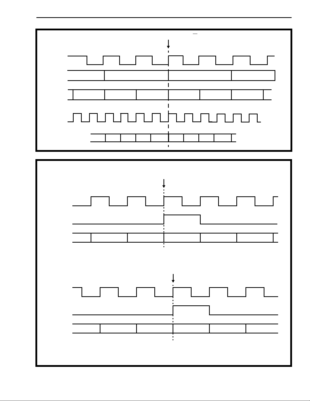
C4/8R1&2
(4 MHz)
Serial I/O
2 Mbps
Serial I/O
4 Mbps
C4/8R1&2
(8 MHz)
Serial I/O
8 Mbps
Frame Boundary Established by
Ch. 31 Bit 1
Ch. 63 Bit 2 Ch. 63 Bit 1 Ch. 63 Bit 0 Ch. 0 Bit 7 Ch. 0 Bit 6 Ch. 0 Bit 5
ch.127
b3
Ch. 31 Bit 0
ch.127
b2
ch.127
b1
ch.127
b0
ch. 0
b7
F0
Ch. 0 Bit 7
ch. 0
b6
ch. 0
b5
ch. 0
b4
Figure 3 - Serial Port Interface Functional Timing
Frame Boundary Established by PPFRi
Ch. 0 Bit 6
PCKR
PPFRi
PDi0-7
PCKR or PCKT
(TCP bit = 0)
PPFTi/o
(PPFP bit =1)
PDo0-7
Notes: In TM1, 2 and 4 PPFRi and PPFT are not simultaneous.
Terminal count “n” = 2429, 2047, or 809.
Ch. n-2 Ch. n-1 Ch. n Ch. 0 Ch. 1 Ch. 2
Frame Boundary Established by PPFTi/o
Ch. n-2 Ch. n-1 Ch. n
Ch. 0 Ch. 1 Ch. 2
Figure 4 - Parallel Data Port Functional Timing
2-237
Page 8

MT90840 Preliminary Information
an address-value in the path’s Data Memory. A given
output time slot is controlled by programming the
Connection Memory control-address with the
address-value of the source input time slot. At the
same control-address the output time slot is enabled
or tri-stated and other per-channel functions set up.
Thus each output time slot is individually controlled,
and any given input time slot might be copied to one,
several, or none of the output time slots.
Transmit Path
The Transmit Path is from the serial inputs, through
the Transmit (Tx) Path Data Memory, to the parallel
outputs (PDo0-7). This path is controlled by the
contents of the Tx Connection Memory. The Tx
Connection Memory is programmed, for each output
time slot, with the address-value of the source
channel to be read out of the Tx Data Memory. Up to
512 channels of serial input can be switched to up to
2430 channels of parallel output.
Transmit Path Connection Memory
The Tx Path Connection Memory is structured as
2430 words of 16 bits. This supports up to 2430 DS0
channels for parallel rates up to 19.44 Mbyte/s (155
Mbps). The Tx Path Connection Memory is accessed
as two-sub memories: High and Low. The
Connection Memory Low (2430 X 8) is the low byte
of the word, and is programmed with the
address-value of the serial-input source channel.
The Connection Memory High (2430 x 8) is the high
byte of the word. Connection Memory High holds the
high-order bit(s) of the source address-value, and is
also programmed to control per-channel functions
such as output driver-enable and programmable
control outputs.
Transmit Path Data Memory
The Tx Path Data Memory is structured as 512
words of 8 bits. Serial input time slots are converted
to parallel bytes and copied to the Tx Path Data
Memory sequentially, serial-stream by serial-stream.
The lowest address of the Tx Path Data Memory is
STi0-channel0, the next is STi0-channel1, and so on.
At 2 Mbps, with 32 channels per STi pin,
STi1-channel0 would be 32 addresses higher than
STi0-channel0. The Tx Path Data Memory is read
out to the parallel outputs by the Tx Connection
Memory.
Receive Path
The Rx Path Connection Memory is programmed, for
each output time slot, with the address-value of the
source channel to be read out of the Rx Path Data
Memory. Up to 2430 channels of parallel input can
be switched to up to 512 channels of serial output.
Each output byte, whether switched data or message
mode data, is read from memory and passed to the
parallel-to-serial converters, and then driven out the
serial port.
Receive Path Connection Memory
The Rx Path Connection Memory is structured as
512 words of 16 bits. This supports up to 512 DS0
channels. The Rx Path Connection Memory is
accessed as two sub-memories: High and Low. The
Connection Memory Low (512 x 8) is the low byte of
the word, and is programmed with the address-value
of the parallel-input source channel. The Connection
Memory High (512 x 8) is the high byte of the word.
Connection Memory High holds the high-order bits of
the source address-value, and is also programmed
to control per-channel functions such as output
driver-enable and direction-control.
Receive Path Data Memory
The Rx Path Data Memory is structured as 2430
words of 8 bits (1 byte). Parallel input time slots are
copied to the Rx Path Data Memory sequentially.
The Rx Path Data Memory is read out to the serial
port by the Rx Path Connection Memory.
Bypass/Parallel-Switching Path
The Bypass/Parallel Switching path is from parallel
input to parallel output. Data received at the parallel
inputs (PDi0-7) is copied to the Rx Path Receive
Memory, and may be passed to the parallel outputs
(PDo0-7) under control of the Tx Path Connection
Memory.
Bypass
In ring timing modes (TM1 and TM2) this is a bypass
path. When the Bypass bit (PPBY) for a given
parallel output channel is set in the Tx Path
Connection Memory, the same-address parallel input
channel is copied (bypassed) to that parallel output
channel. This allows data channels not destined for
the local node to be bypassed to the output port and
down the ring. “Broadcast” channels destined for
every node can also be bypassed, since PPBY is an
output control, and it does not affect the availability
of the Receive Parallel data for switching to the serial
port or monitoring through the CPU interface.
The Receive Path is from the parallel inputs
(PDi0-7), through the Receive (Rx) Path Data
Memory, to the serial outputs. This path is controlled
by the contents of the Rx Path Connection Memory.
2-238
Parallel Switching
In Parallel Switching Mode (TM4) this is a switching
path, and the Tx Path Connection Memory is
Page 9

Preliminary Information MT90840
programmed to switch parallel inputs to parallel
outputs. For each parallel output channel
control-address, the Tx Path Connection Memory is
programmed with the 12-bit address-value of the
desired parallel input channel.
Serial Data Port
The serial port consists of 16 bidirectional serial data
lines (STo0-7, STi0-7), two reference input clock pins
(C4/8R1, C4/8R2), one serial clock output (SPCKo)
and a bidirectional frame synchronization signal (F0i/
o). The STi pins are the default inputs, but the user
can program the direction of the pins on a
per-channel basis in the Rx Path Connection
Memory.
The serial port modes are controlled by the DR bits
and the FDC bit in the IMS register, and are:
• 2.048 Mbps Balanced: 8 inputs and 8 outputs per
serial time slot (FDC = 0),
• 2.048 Mbps Add/Drop: 16 serial I/O individually
programmed per time slot (FDC = 1),
• 4.096 Mbps: 8 inputs and 8 outputs per time slot,
• 8.192 Mbps: 4 inputs and 4 outputs per time slot.
Figure 3 shows the different data rate configurations
for the MT90840 serial port.
In addition the user can specify the placement and
polarity of the output frame pulse F0o as ST-BUS or
GCI compatible, using the SPFP bit in the GPM
register. In TM1, the MT90840 automatically detects
ST-BUS or GCI serial bus modes, based on the
polarity of F0i. The user can also specify which of the
two input clock pins - C48R1 or C48R2 - to use as
the serial port clock source, using the C4/8R bit in
the TIM register.
The user can define the direction of each time slot of
the serial port. This per-channel direction control
feature is controlled by the DC bit in the Rx Path
Connection Memory High. This is ideal for
applications in Computer Telephony Integration (CTI)
where per-channel direction control is required within
telephony servers.
2.048 Mbps Balanced Mode
The 2.048 Mbps Balanced mode has 8 inputs and 8
outputs active during each serial-byte-period or “time
slot”. At 2.048 Mbps, each STi/o pin has 32 8-bit
channels per 125 µsec frame, with each individual
channel at 64 kbps. (1/125µsec X 8 bits = 64 kbps,
32 x 64 kbps = 2.048 Mbps). This mode supports
256 serial input channels and 256 serial output
channels. This mode is “balanced” in that there are
always 8 inputs and 8 outputs during a time slot. If a
specific time slot in an output stream (e.g.
STo0-channel7) is programmed in the Rx Path
Connection Memory as an input, the corresponding
time slot on the equivalent input stream (i.e.
STi0-channel7) is automatically an output. The serial
clock for this mode is 4.096 MHz.
2.048 Mbps Add/Drop Mode
The 2.048 Mbps Add/Drop mode (FDC bit high) has
16 bidirectional streams active during each time slot.
This mode allows up to 512 input channels, or up to
512 output channels, or any mix of channels totalling
512 channels. Per-channel direction control in the Rx
Connection Memory specifies the direction of all 512
serial channels from STo0-channel0 up to
STi7-channel31.
4.096 Mbps Mode
The 4.096 Mbps mode has 8 inputs and 8 outputs
active during each time slot. At 4.096 Mbps each
STi/o pin has 64 channels of 64 kbps. This mode
supports 512 serial input channels and 512 serial
output channels. The serial clock is 4.096 MHz.
Per-channel direction control in this mode is the
same as the 2.048 Mbps balanced mode.
8.192 Mbps Mode
The 8.192 Mbps mode has 4 inputs and 4 outputs
active during each serial byte period. At 8.192 Mbps,
each STi/o pin has 128 channels. This mode
supports 512 serial input channels and 512 serial
output channels. The serial clock for this mode is
8.192 MHz. Per-channel direction control in this
mode is the same as the 2.048 Mbps balanced
mode.
Serial Port Clock Signals
Depending on the Timing Mode selected, the serial
port clock is either an input, or an output derived
from a reference clock. In modes where the serial
clock is derived by the MT90840 from a reference
clock, the serial port clock output appears at SPCKo.
The reference clock is either PCKR (if INTCLK is
high), or one of C4/8R1 or C4/8R2. The C4/8R bit of
the Timing Mode Register is used to select which of
C4/8R1 or C4/8R2 will be the clock source or
reference pin. Switching between clock sources
during device operation will cause temporary TDM
data errors.
Internal 4.096 MHz Clock Generator
For TM2 applications running at 19.44 or 16.384
MHz rates on the parallel port, an internal divider can
be used to generate a 4.096 MHz clock from the
PCKR clock input. The internal divider can not be
used in applications where the parallel port operates
at 6.480 Mbyte/s rates. The INTCLK bit in the TIM
2-239
Page 10

MT90840 Preliminary Information
Register enables the internal divider, and the SPCKo
output (and internal 4.096 MHz clocks) are driven by
the clock divided-down from PCKR. At 16.384 MHz,
this is a simple divide-by-4, and the SPCKo output
jitter will depend on the PCKR input jitter. At 19.44
MHz, the SPCKo output jitter will be larger as the
divider switches between rising and falling edges of
PCKR. The serial port timing and F0o frame pulse
are tightly slaved to PPFRi when INTCLK is set high.
Serial Frame Pulse
In TM1, the MT90840 receives the frame reference
(F0i) from an external source, and the MT90840
senses the polarity of the frame pulse and adapts the
device timing to the appropriate (ST-BUS or GCI)
format.
In TM2 and TM3, the MT90840 outputs the serial
port frame pulse (F0o). Positive (GCI) or negative
(ST-BUS) frame pulse formats, and the associated
clock polarity, can be selected for the F0o signal by
programming the SPFP bit in the GPM Register. This
flexibility allows the MT90840 to be employed with
different serial bus formats.
In applications which require a large number of serial
channels in TM2, it is possible to operate multiple
MT90840s in parallel using the SFDI control bit (in
the TIM register). To allow the MT90840s to
synchronize their internal timing, all of the MT90840s
are connected to the same C4/8 reference source,
and one MT90840 in normal TM2 (SFDI set low)
supplies F0 to one or more MT90840s in TM2 with
SFDI set high. With SFDI set high, F0 becomes an
input, and this allows the MT90840 driving F0 to
control the timing of one or more other MT90840s. If
the internal 4.096 MHz clock divider is used (INTCLK
high) it is not necessary to use the SFDI control, as
the serial port timing and F0o frame pulse of each
parallel MT90840 will be tightly slaved to PPFRi
when INTCLK is set high.
Should the input framing at F0i cease while the C4/8
clock continues to run, the MT90840 will continue to
function as if the frame pulse was asserted after the
normal number of clock cycles (free run). If F0i
re-commences the MT90840 will immediately sync to
F0i, but changes in the F0i interval will temporarily
disrupt the TDM data streams. If the F0i input is held
asserted, the serial I/O will “lock up” and operation
will be disrupted.
Parallel Data Port
The MT90840 parallel port is composed of an 8-bit
wide Parallel Data Output Port (PDo0-7), a 4-bit wide
Control output port (CTo0-3), an 8-bit wide Parallel
Data Input Port (PDi0-7), a Receive Frame sync
signal (PPFRi) and a Transmit Frame sync signal
(PPFT), and Transmit (PCKT) and Receive (PCKR)
Clocks.
The Parallel Port Rates are controlled by the PPS
bits in the IMS register, and are:
• 19.44 Mbyte/s (2430 channels),
• 16.384 Mbyte/s (2048 channels), and
• 6.48 Mbyte/s (810 channels).
The user can further specify the features of the
parallel TDM port, including:
• the edge of the parallel port clock used to transmit
data and PPFTo (see TCP bit in the TIM register),
• the polarity of the Parallel Port Frame Transmit
pulse PPFT (see PPFP bit in the GPM register),
• the use of PPFT (normally an output) as an input in
TM1, if the application requires multiple MT90840
devices to operate in parallel (see PFDI bit in the TIM
register).
The parallel port of the MT90840 is flexible enough
to interface to a variety of applications. It can be
connected to a framer to access a serial transport
backbone running at up to 155 Mbps. It can be
connected to a backplane-type parallel bus. It can
share a parallel bus with other devices, using the
control outputs (CTo0-3) and the per-channel tristate
function to share access to the bus.
Parallel Por t Clock Signals and Framing
The MT90840's PPFRi (Parallel Port Frame pulse
Receive input) and PPFTi/o (Parallel Port Frame
pulse Transmit i/o) signals synchronize the MT90840
to the high speed data frame. Receive data is
clocked in at the Parallel Data inputs (PDi0-7) by the
Parallel port Receive ClocK (PCKR), as framed by
Receive Parallel Port Frame input (PPFRi). In TM2,
TM3 and TM4, PCKR also clocks the Parallel Data
outputs (PDo0-7), with the framing in TM2 and TM4
indicated by the PPFTo output. In TM1, the Parallel
Data outputs are clocked out by PCKT, with the
framing indicated by PPFTo. Alternatively, the
Transmit framing can be controlled by the PPFTi
input if the PFDI bit in the TIM register has been set
high, to enable multiple MT90840s to operate in
parallel in TM1.
Should the input framing at PPFRi cease while the
PCKR clock continues to run, the MT90840 will
continue to function as if the frame pulse was
asserted after the normal number of clock cycles
(free run). If PPFRi re-commences, the MT90840 will
immediately sync to PPFRi, but any change in the
framing interval will temporarily disrupt the TDM data
2-240
Page 11
Preliminary Information MT90840
streams, and trigger the PPCE interrupt bit. PPCE
will be triggered by PPFRi moving from the expected
time, but PPCE will not be triggered by a missing
PPFRi. If the PPFRi input is held asserted, the
parallel I/O will “lock up” and operation will be
disrupted (including CPU access to the TPCM).
The PPFTi framing in TM1 with PFDI=1 operates
similarly, using PCKT, but the PPCE interrupt does
not monitor PPFTi. Instead, the TXPAA bit indicates
that the PPFTi input is out of phase with F0i.
Output Driver Enable Control Capability
The MT90840 provides a bit (ODE) in the IMS
Register that places all data outputs of the device
(parallel and serial) in a high impedance state. The
ODE bit (Output Drive Enable) is automatically set
low by the reset input pulse applied to the device
during system power up. When low, the ODE bit
disables all TDM outputs of the MT90840 while
Connection Memory initialization is performed by the
CPU. This function is useful to avoid data collision
when the MT90840 is sharing a transmit parallel bus
with other devices. When ODE is set high, individual
parallel and serial port time slots are controlled by
the OE bits in TPCM High and RPCM High.
Timing and Switching Control
The MT90840 supports four major timing/switching
modes:
• TM1/Ring Master: PDo timing slaved to STi/o
timing, Receive Path has elastic buffer enabled;
• TM2/Ring Slave: STi/o timing slaved to PDi timing,
fixed delay in Receive Path;
• TM3/Bus Slave: PDo and PDi tied together, STi/o
timing slaved to parallel bus timing;
• TM4/Parallel Switching: 2430 (or 2048) channel
switching from PDi to PDo.
The TM1-0 bits in the TIM Register are used to
select the timing modes. The PFDI and SFDI bits in
the same register can be used to enable
parallel-device sub-modes of TM1 and TM2
respectively. In all MT90840 timing modes, the
throughput delay when performing time interchange
functions of grouped channel data is constant,
maintaining the frame integrity of the input and
output data.
Timing Mode 1 (TM1) - Ring Master
Asynchronous Parallel Por t With ST-BUS Clock
Master
Timing Mode 1 is used where the main TDM clock
reference resides on the serial port side of the
system. (An example is a node which is the clock
master on a ring network.) Timing on the transmit
parallel port is tightly tied to the serial port. The
receive parallel port timing is elastic; there is an
elastic buffer in the Receive Path and the Bypass
Path. See Figure 5a for a connection example.
In TM1, the MT90840 receives the serial port frame
pulse (F0i) and serial clock (C4/8R1 or C4/8R2). The
MT90840 then generates the parallel port output
frame pulse (PPFTo) synchronized to F0i. The
transmit parallel port is fixed in phase relative to the
serial port. (A fixed offset of 3.8 µsec exists between
F0i and PPFTo due to serial-to-parallel conversion.)
The transmit path does not provide an elastic buffer,
and therefore the parallel port TX clock (PCKT) must
be tightly locked (in frequency) to the serial port C4/8
and F0i clocks. (Jitter less than +/- 100nsec.)
The receive parallel port timing may be of any phase
relative to the serial and transmit-parallel ports in
RX Clock
8 kHz RX
Data RX
8
8 kHz TX
8
Data TX
MT90840
PCKR
PPFRi
PDi0-7
PCKT
PPFTo
PDo0-7
TX Clock
STi0-7
STo0-7
F0i
C4/8R1
CPU
STi/o 0-7
8
STi/o 0-7
8
8 kHz
4.096
or 8.192 MHz
PLL
Figure 5a - Timing Mode 1 Configuration
ST-BUS
Components
8 kHz
Source
2-241
Page 12
MT90840 Preliminary Information
TM1. This allows for flexible round-trip data delays in
star or ring type networks. An elastic buffer on the
receive parallel port compensates for the difference
in phase between PPFRi/PCKR and F0i/C4. The
elastic buffer can also tolerate up to 50 µsec +/- 25
µsec) of clock drift and jitter before the buffer
re-syncs and Rx Path data is corrupted. (Data
corruption is flagged by the FSA interrupt source.)
The Bypass Path data (PDi to PDo) also passes
through the elastic buffer in TM1.
In TM1, the MT90840's SPCKo clock output is not
used.
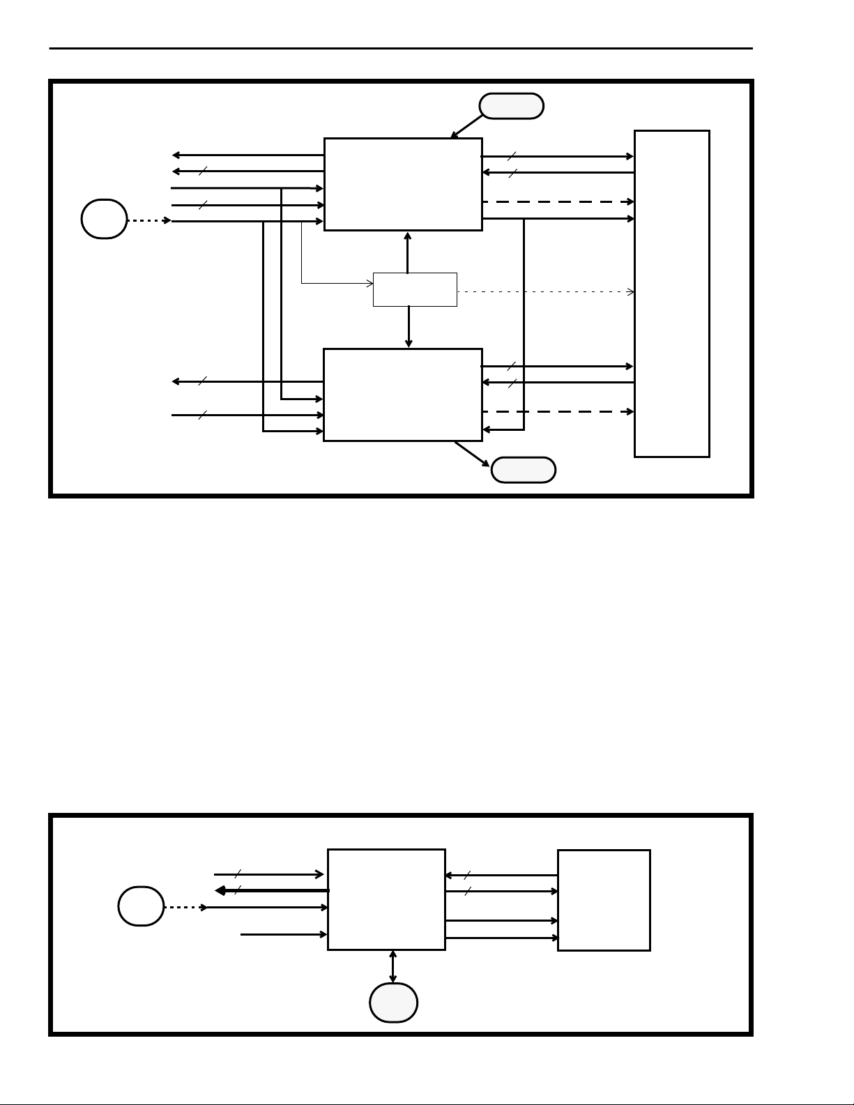
TM1 Multiple-MT90840 Sub-Mode (PFDI)
For TM1 applications which require more serial
channels than are provided by a single MT90840, it
is possible to operate multiple MT90840 in parallel.
To do this, one MT90840 must control the
F0i-to-PPFTo timing (normal TM1), and the
remaining MT90840s must synchronize to the first by
using PPFTi as an input reference. The device
providing the reference will have the PFDI bit in the
TIM Register set low (normal TM1). All other
MT90840s will have PFDI set high (forcing PPFT to
be an input).
Figure 5b shows this mode using two MT90840s;
additional MT90840s (with PFDI set high) may be
added. This sub-mode allows the serial ports of the
multiple MT90840 to share one timing source, and
the synchronized parallel output ports to be
connected together on one bus.
The TM1 Multiple-MT90840 sub-mode is not
available for operation at 6.48 Mbyte/s.
Timing Mode 2 (TM2) - Ring Slave
Asynchronous Parallel Por t With ST-BUS Clock
Slave
Timing Mode 2 is used where the main TDM clock
reference resides on the parallel port side of the
system. (An example is a node on a ring which is
slaved to the ring clock.) Timing on the serial port is
tightly tied (slaved) to the receive parallel port, and
the transmit parallel port is clocked by the receive
parallel port clock. In TM2, the PCKT input is not
used. See Figure 6a for a connection example.
In TM2, the MT90840 timing is controlled by the
parallel port frame pulse (PPFRi) and clock (PCKR).
The MT90840 generates the parallel port output
frame pulse (PPFTo) and the serial port output frame
pulse (F0o) locked to PPFRi. Both the transmit
parallel port and the serial port are fixed in phase
relative to the receive parallel port, and therefore no
elastic buffer is required. A fixed offset exists
between PPFRi and F0o due to parallel-to-serial
conversion, and between F0o and PPFTo due to
serial-to-parallel conversion delay. Total offset
between PPFRi and PPFRo is about 12 µsec (and
the Bypass Path data delay is therefore also about
12 µsec).
2-242
8
8
RX Clock
8 kHz RX
RX Data
TX Clock
8 kHz TX
TX Data
TX Clock
8 kHz TX
8
Data TX
PCKR
PPFRi
PDi0-7
PCKT
PPFTo
PDo0-7
PCKR
PPFRi
PDi0-7
PCKT
PPFTi
PDo0-7
PFDI = 0
CPU
PFDI = 1
MT90840
STi0-7
STo0-7
F0i
C4/8R1
MT90840
STi0-7
STo0-7
F0i
C4/8R1
STi/o 0-7
8
STi/o 0-7
8
8 kHz
4.096
or 8.192 MHz
STi/o 0-7
8
STi/o 0-7
8
8 kHz
4.096
or 8.192 MHz
Figure 5b - TM1 Multiple-MT90840 Configuration
ST-BUS
Components
8 kHz
Source
TX Clock
PLL
Page 13
Preliminary Information MT90840
The transmit path does not provide an elastic buffer,
and therefore the serial port clock must be tightly
locked (in frequency) to the parallel port clock
(PCKR). (Jitter less than +/- 100nsec.) This may be
achieved in one of two ways: use of the internal clock
divider (INTCLK set high), or use of an external PLL
or DPLL, with C4 phase-correction performed by the
MT90840.
Internal 4.096 MHz Clock Divider
For TM2 applications at 19.44 or 16.384 MHz rates
on the parallel port, and 4.096 MHz on the serial
port, the internal clock divider can be enabled. The
clock divider can generate the required serial port
clock outputs from the parallel port clock inputs.
When enabled in TM2, the clock divider will provide
4.096 MHz (SPCKo) and 8 kHz (F0o) timing to the
serial port that is rigidly locked to the PCKR and
PPFRi clocks at the parallel port. The clock divider is
enabled by setting the INTCLK bit high (in the TIM
Register). The clock divider can not be used in
applications where the parallel port operates at
6.480 Mbyte/s rates.
External PLL and C4 Phase-Correction
The MT90840 also supports the use of an external
PLL (e.g. MT9041/2) to generate 4.096 or 8.192 MHz
from the parallel port timing reference. At 4.096 MHz
the generated clock must be input to the MT90840
(at C4/8R1 or C4/8R2) for phase monitoring and
correction. The phase-corrected 4.096 MHz clock is
then output on the SPCKo pin. Should the phase of
the C4clock input (relative to the PPFRi framing
input) drift more than approximately +/- 100nsec, the
MT90840 will apply an additional correction and
indicate possible data corruption with the RXPAA
interrupt source. At 8.192 MHz, the generated clock
is input to the MT90840 (at C4/8R1 or C4/8R2), and
is also supplied directly to the serial bus (the SPCKo
output is not used at 8.192 MHz). The serial port
frame pulse (F0o) will be slaved to the parallel port
frame pulse (PPFRi), and will be clocked out by
SPCKo, or the 8.192 MHz clock, as appropriate.
TM2 Multiple-MT90840 Sub-Mode (SFDI)
For TM2 applications which require more serial
channels than are provided by a single MT90840, it
is possible to operate multiple MT90840s in parallel.
Multiple-MT90840 operation is automatic if INTCLK
is selected, but if an external PLL is used, the serial
port timing of the MT90840s must be synchronized.
To do this, one MT90840 controls the PPFRi-to-F0o
timing and C4 phase-control (normal TM2), and the
remaining MT90840s must synchronize to the first by
using F0 as an input reference. The device providing
the reference will have the SFDI bit in the TIM
Register set low (normal TM2). All other MT90840s
will have SFDI set high (forcing F0 to be an input).
Figure 6b shows this mode using two MT90840s;
additional MT90840s (with SFDI set high) may be
added. This sub-mode allows the serial ports of the
multiple TM2 MT90840s to share one timing source.
The transmit parallel port outputs are always
synchronized to PPFRi in TM2, so the multiple
MT90840s can also be connected together on one
parallel output bus.
The TM2 Multiple-MT90840 sub-mode is not
available for operation at 6.48 Mbyte/s.
MT90840
8 kHz TX
Data TX
8
TX/RX Clock
8
Data RX
8 kHz
Source
Note: the use of an external PLL is optional at 4.096 MHz (2.048 Mbps and 4.096 Mbps)
8 kHz RX
PPFT
PDo0-7
PCKR
PDi0-7
PPFRi
C4/8R1 & 2
4.096 MHz or
8.192 MHz
PLL
STi0-7
STo0-7
SPCKo
F0o
Figure 6a - Timing Mode 2 Configuration
CPU
8
8
4.096 MHz
8 kHz
(8.192 MHz)
STi/o 0-7
STi/o 0-7
ST-BUS
Components
2-243
Page 14
MT90840 Preliminary Information
CPU
MT90840
8 kHz
Source
8
8
8 kHz TX
Data TX
Data RX
8 kHz RX
TX/RX Clock
PPFT
PDo0-7
PCKR
PDi0-7
PPFRi
SFDI = 0
C4/8R1 & 2
PLL
STi0-7
STo0-7
SPCKo
F0o
4.096 MHz or
8.192 MHz
8
8
STi/o 0-7
STi/o 0-7
4.096 MHz
8 kHz
(8.192 MHz)
ST-BUS
Components
8
8
Data TX
Data RX
PPFT
PDo0-7
PCKR
PDi0-7
PPFRi
Figure 6b - TM2 Multiple-MT90840 Configuration
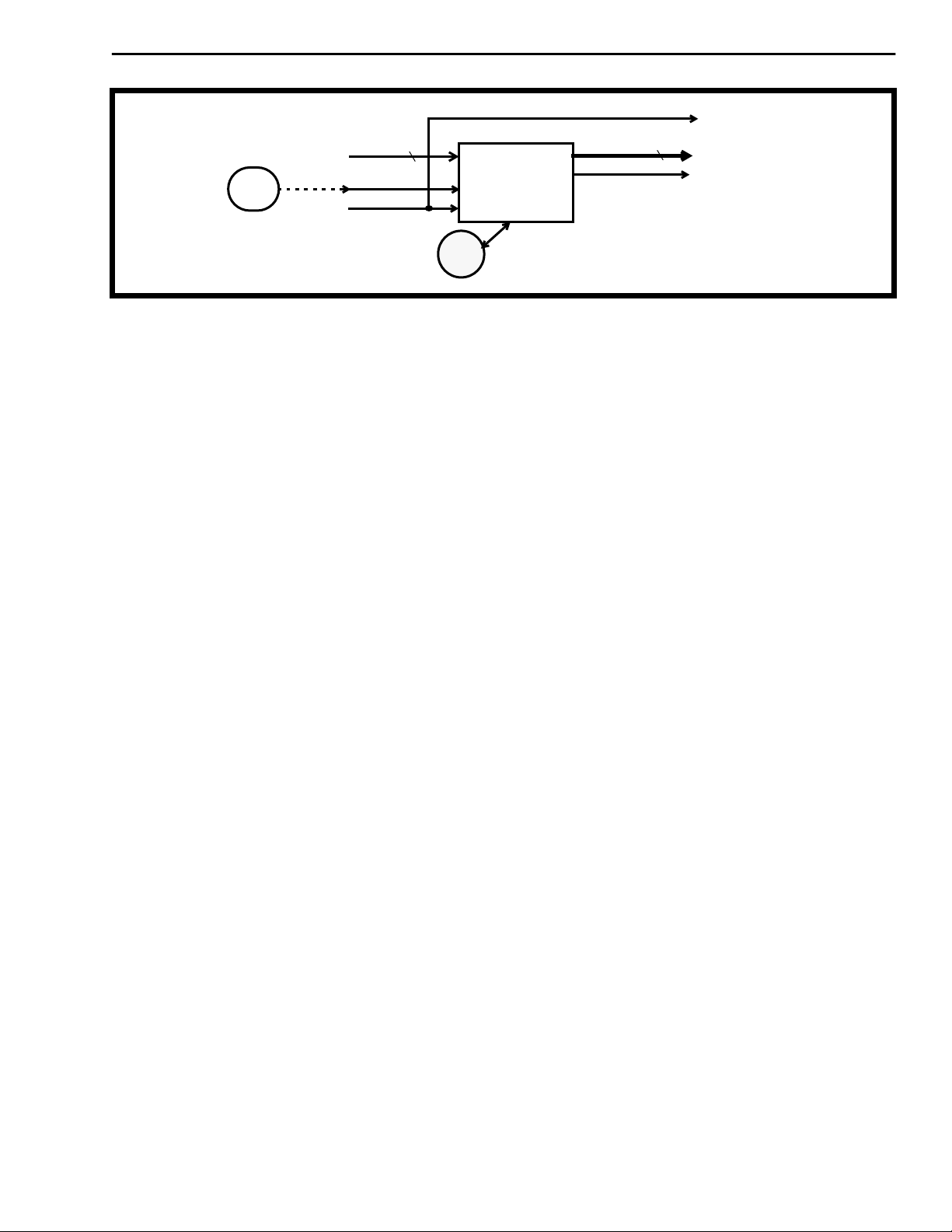
Timing Mode 3 (TM3) - Bus Slave
Synchronous Parallel Por t With ST-BUS Clock Slave
Timing Mode 3 is used where the main TDM clock reference resides on the parallel port side of the system,
and where the receive parallel port and the transmit
parallel port are aligned. (An example is a node on a
backplane.) Timing on the serial por t is tightly tied to
the receive parallel port, and the transmit parallel
port is clocked by the receive parallel port clock. In
TM3, PCKT and PPFTo are not used. See Figure 7
for a connection example.
In TM3, the MT90840 timing is controlled by the
parallel port frame pulse (PPFRi) and clock (PCKR).
C4/8R1 & 2
SFDI = 1
MT90840
STi0-7
STo0-7
SPCKo
F0i
8
8
CPU
STi/o 0-7
STi/o 0-7
4.096 MHz
The MT90840 generates the serial port output frame
pulse (F0o) locked to PPFRi. TM3 is similar to TM2
with two main differences: the parallel Bypass Path is
disabled, and the parallel port receive and transmit
buses are synchronized and both aligned with
PPFRi. A fixed offset exists between F0o and PPFRi
due to serial-to-parallel conversion. The MT90840
will align F0o so that it proceeds PPFRi by 3.8 µsec.
In TM3 the internal clock divider circuit is always
enabled, regardless of the state of the INTCLK bit
(C4/8R1 and C4/8R2 are unused). Therefore TM3 is
limited to 19.44 and 16.384 Mbyte/s parallel port
rates, and 2.048 and 4.096 Mbps serial port rates.
2-244
8 kHz
Source
Aligned
Frames
MT90840
8
8
8 kHz REF
RX/TX Clock
PDi0-7
PDo0-7
PPFRi
PCKR
STi0-7
STo0-7
SPCKo
CPU
8
8
F0o
Figure 7 - Timing Mode 3 Configuration
STi/o 0-7
STi/o 0-7
8 kHz
4.096 MHz
ST-BUS
Components
Page 15
Preliminary Information MT90840
Clock Reference
Parallel Data Out
8
TX 8 kHz REF
Parallel Data In
8 kHz
Source
8
8 kHz RX
19.44 or 16.384 MHz (RX)
Figure 8 - Timing Mode 4 Configuration
CPU
PDi0-7
PPFRi
PCKR
MT90840
PDo0-7
PPFTo
Timing Mode 4 (TM4) - Parallel Data Switching
Timing Mode 4 is used to provide switching of up to
2430 parallel input channels to the same number of
parallel output channels. Parallel TDM data is
clocked in at PDi0-7 by PCKR, framed by PPFRi.
Switching is performed as programmed in the Tx
Path Connection Memory, and data is output on
PDo0-7, framed by PPFTo and clocked by PCKR.
See Figure 8 for connection details.
In TM4, PPFTo and PDo0-7 are offset (delayed) from
PPFRi and PDi0-7 by a fixed 4 clock cycles (3.5
clock cycles if the TCP bit is high). All the serial port
data and timing signals, and PCKT, are unused in
TM4. The internal clock divider is used to generate
an internal C4 clock to allow CPU reads from the
RPDM. TM4 is only available for 19.44 and 16.384
Mbyte/s rates.
MT90840 Throughput Delay
In many isochronous applications it is important to
know and/or limit the delay of data. Table 1
summarizes the data throughput delay values for all
timing modes of the MT90840. It is worth noting that
the worst-case “round-trip” delays are not as large as
the sum of the worst-case delays on the individual
links. This is shown by the last 5 rows of Table 1,
which give the delays for some representative two
MT90840 setups.
these per-channel features are Bypass, Control
Outputs, Output Enable, and Message Mode. O n the
serial port the per-channel features are Output
Enable, Message Mode and Direction Control. These
functions are generally available in all of the data
rates and timing/switching modes.
Per-channel Bypass on the Parallel Port
This feature, when enabled, causes the specific
individual parallel output channel at PDo to transmit
the data received at the same number input channel
at PDi. This can be used to perform a bypass (on a
ring) or a loopback (in a star). This feature is only
provided in Timing Modes 1 and 2. In TM2 the
data-delay from PDi to PDo is fixed (as is the delay
between PPFRi and PPFT). In TM1 the data-delay is
elastic (and dependent on the timing of PPFRi and
F0i).
The per-channel bypass feature is controlled by the
PPBY bits of the TPCM High as explained in the
register section. If the PPBY bit is HIGH at a specific
TPCM address, the corresponding parallel output will
transmit the data received in the corresponding input
channel. When the PPBY bit is LOW, the
corresponding output channel can be used for
message-mode data, or for switched-data from the
serial port. A bypass input channel is still copied to
the Receive Path Data Memory, and may also be
switched to the serial port, or read by the CPU from
the Receive Path Data Memory.
MT90840 Per-channel Functions
Several functions of the MT90840 are programmable
for each individual parallel channel or serial channel.
Per-channel functions on the parallel port side are
programmed in the Transmit Path Connection
Memory High (TPCM High), and per-channel
functions on the serial port interface are
programmed in the Receive Path Connection
Memory High (RPCM High). On the parallel port
The MT90840 per-channel output-enable and
message-mode bits have higher priority than the
PPBY bit.
Per-channel Control Outputs on the Parallel Port
The MT90840 provides four control outputs
(CTo0-CTo3) which are synchronized to the parallel
port output timing. Each of the CTo output pins is
controlled by the CT0-3 bits of the TPCM High. (The
CTo0 pin and bit are programmed with the Output
Enable data.) The contents of the CTo bit in each
2-245
Page 16

MT90840 Preliminary Information
Mode Data Rates Minimum Delay Total Throughput Delay
TM1, TM2,
or TM3 S/P
All Dmin = 7.7 µsec
Note 1
TM1P/S All Dmin = ELDmin
= 4.4 µsec
Note 2
TM2 P/S All Dmin = 4.3 µsec
Note 1
TM3 P/S All Dmin = 1 frame -
7.7 µsec
= 117.3 µsec
TM1 P/P
(Bypass)
All Dmin = 12 µsec +
1 frame
= 137 µsec
Note 2
TM2 P/P
(Bypass)
19.44 Mbyte/s
16.384 Mbyte/s
Note 3
6.480 Mbyte/s
TM4 P/P
(Switching)
19.44 & 16.384
Mbyte/s
Dmin = {3.5 or 4}
PCKR cycles
(TCP bit = 1 or 0)
TM1 S/P +
TM2 P/S
All Dmin = 12 µsec +
1 frame
= 137 µsec
D = Dmin + 1 frame + Po - Si = 132.7 µsec + Po - Si
Min. 7.7 µsec, Avg. 133 µsec, Max. 258 µsec
D = 1 frame + ELD + So - Pi = 125µsec + ELD + So - Pi
Min. 4.4 µsec, Max. 379 µsec
D = Dmin + 1 frame + So - Pi = 129.3 µsec + So - Pi
Min. 4.3 µsec, Avg. 129 µsec, Max. 254 µsec
T = Dmin + 1 frame + So - Pi = 242.3 µsec + So - Pi
Min. 117 µsec, Avg. 242 µsec, Max. 367 µsec
D = 7.7 µsec + 1 frame + ELD
Min.137 µsec, Max. 262 µsec
D = {235 or 235.5} PCKR cycles = 12 µsec
D = {199 or 199.5} PCKR cycles = 12 µsec
D = {80 or 80.5} PCKR cycles = 12 µsec
D = Dmin + 1 frame + Po - Pi
Min. < 0.3 µsec, Avg. 125 µsec, Max. 250 µsec
D = 12 µs + 2 frames + Transmission + So - Si
= 262 µsec + Transmission + So - Si
TM2 S/P +
TM1 P/S
All Dmin = 12 µsec +
1 frame
D = 12 µsec + 2 frames + Transmission + ELD + So - Si
= 262 µsec + Transmission + ELD + So - Si
= 137.4 µsec
TM1 S/P +
TM2 P/S +
TM2 S/P +
All Dmin = 4 frames
= 500 µsec
D = (2 X 12) µsec + 4 frames + 2 X Transmission + ELD
+ So - Si = {5 or more integral frames} + So - Si
(Note 4)
TM1 P/S
TM1 S/P +
TM2
Bypass +
TM1 P/S
TM3 S/P +
TM3 P/S
All Dmin = 2 frames
= 250 µsec
D = (3 X 12) µsec + 2 frames + 2 X Transmission + ELD
+ So - Si
= {3 or more integral frames} + So - Si
(Note 4)
All Dmin = 250 µsec D = (7.7 + 117.3) µsec + 2 frames + So - Si
= 375 µsec + So - Si
Min. 250 µsec, Avg. 375 µsec, Max. 500 µsec (Note 4)
Table 1 - MT90840 Throughput Delay Summary
Naming rules:
ELD: ELastic Delay, measured from PPFRi to F0i (4.4 to 129.4 µsec).
P/S:Parallel-to-Serial data path.
Pi:Parallel Input channel time, expressed in delay after PPFRi (0 to 125 µsec).
Po:Parallel Output channel time, expressed in delay after PPFTi/o (0 to 125 µsec).
S/P:Serial-to-Parallel data path.
Si:Serial Input channel time, expressed in delay after F0i/o (0 to 125 µsec).
So: Serial Output channel time, expressed in delay after F0i/o (0 to 125 µsec).
Transmission:The delay due to electronic circuits and physical media connecting the parallel ports of two MT90840s. (Assumed to be
negligible in TM3.)
Note 1: Exact P/S or S/P delay depends on relative positions of PPFRi and F0 +/- 120 nsec tolerance).
Note 2: Actual TM1 P/S and P/P delay depends on elastic position of PPFRi with respect to F0i (see ELD definition).
Note 3: Bypass delay in TM2: PPFT and PDo ch.0 are co-incident with PDi ch.235 at 19.44 MHz, ch.199 at 16 MHz, and ch.80 at 6.48
MHz. (TCP = 1 delays PDo ch.0 an extra half clock-cycle in TM2).
Note 4: “Round-tr ip” delay from/to serial por ts with the same F0 is always an integral number of frames (plus switching: So - Si).
2-246
Page 17

Preliminary Information MT90840
Output Frame Boundary Established by PPFT
PPFT
PDo7-0
Byte Timing
CTo0-3
Outputs
Note: For applications at 16.384 and 6.48 Mbyte/s, only 2048 and 810 positions are usable, in the TPCM.
Channel 2428
TPCM High, CTn bit
address 2428
Channel 2429
TPCM High, CTn bit
address 2429
Channel 0
TPCM High, CTn bit
address 0
Figure 9 - Parallel Port Control Outputs, CTo0-3
DC=0 for STo 0 channel 1
O/P
STi0
. . . . .
0123 3029 31
I/P
MT90840
DC=1 for STo 0 channel 29
0123 3029 31
I/P
Figure 10 - Balanced Per-Channel Serial Direction Control as Determined by DC Bit
TPCM High location is output on the corresponding
CTo pin once every frame. See Figure 9. The control
outputs can be used to control other devices, such
as buffers, to allow shar ing of the parallel port data
bus.
Per-channel Direction Control on the Serial Por t
The MT90840 provides the ability to use any nominal
output serial channel as an input or as an output.
The direction of each output serial channel is
controlled by the DC bit in the appropriate byte of the
Receive Path Connection Memory High (RPCM
Per-channel Tr i-state (Serial and Parallel)
The MT90840 provides per-channel tri-state of the
output pins on both the serial and parallel port. The
OE bit in each address of the TPCM and RPCM
High). When DC is HIGH the matching channel is an
output. The per-channel direction control feature of
the MT90840 can be activated in one two modes:
balanced, or add/drop operation.
determines if data will be driven during a par ticular
time slot, or if the pin will be placed in a
high-impedance state during that time slot. The OE
bit overrides all other per-channel control bits.
• Balanced Operation (all serial data rates)
This mode is enabled when the FDC bit in the IMS
Register is LOW. In this mode, each of the DC bits
controls two serial channels: the nominal output and
Per-channel Message Mode (Serial and Parallel)
The MT90840 provides per-channel message mode
capability on both the serial and parallel port. The
MC bit in each address of the TPCM and RPCM
determines if the Connection Memory Low byte is to
be used as an address, or as data to be output on
the particular channel (message mode). When the
MC bit is HIGH, the Connection Memory Low byte is
used as message data. As well as driving message
data on the serial (RPCM) and parallel (TPCM)
ports, the MT90840 allows the CPU to read serial or
the nominal input. If a channel on a nominal output
serial stream (STo0-7) is re-defined as an input, the
same-number channel on the matching input stream
(STi0-7) will be defined as an output. For example, if
channel 0 on STo7 is programmed as an input
(DC=0), then channel 0 on STi7 is defined as an
output. Each DC-bit’s state controls the direction of a
channel on the nominal output stream (DC is HIGH
for output), and inverse-sense controls a channel on
the nominal input stream (DC is LOW for output).
This is shown in Figure 10.
parallel data channels from the TPDM or RPDM.
Applications for message mode include digital
silence, proprietary signalling, and creating fixed 8
kHz framing patterns.
• Add/Drop Operation (2.048 Mbps only)
This mode is enabled when the FDC bit in the IMS
Register is HIGH. In Add/Drop mode all channels on
Channel 1
TPCM High, CTn bit
address 1
STo0
O/P
. . . . .
2-247
Page 18

MT90840 Preliminary Information
all 16 serial streams can be individually controlled,
so that up to 512 channels can be either transmitted
or received. As an example, if all DC bit locations of
RPCM High are set HIGH, all 512 channels on
STo0-7 and STi0-7 will be configured as outputs. If
all DC bits are LOW, then all 512 channels will be
configured as inputs. In Add/Drop mode all 512
serial channels are copied into the Transmit Path
Data Memory, as inputs, regardless of the DC or OE
bits. This has the effect of a “copy-back” of all serial
outputs.
For more details on per-channel control functions for
the serial and parallel data ports, see the TPCM
High and RPCM High bits definition in the Register
Description section.
Serial Data Memory Addressing
Serial Input
Channel
STi0, Ch0
STi0, Ch1
.
.
STi7, Ch30
STi7, Ch31
Note: Only 256 memory
locations.
Figure 11a - 2.048 Mbps Balanced Mode TPDM
TPDM
Address
000H
001H
0FEH
0FFH
Addressing
CPU Port Addressing:
Address BusCAR
06543210
Stream
TPCM Contents:
765
Stream
Bits 7:5 select one of 8 streams.
Bits 4:0 select one of 32
channels per stream.
Channel
43
Channel
21
0
The serial port mode determines the number of
channels per stream, the number of streams, and the
direction-control operation. Therefore the way in
which serial data is addressed in the internal
memory space must change with the serial port
mode. Because of this, it is necessary to select the
serial port mode (with DR1-0 and FDC in the IMS
register) before programming the Receive Path
Connection Memory.
2.048 Mbps Balanced Mode
The 2.048 Mbps Balanced mode has 8 serial input
and 8 serial output streams, and 32 channels per
stream. Therefore 3 bits are used to address the 8
streams, and 5 bits are used to address the 32
channels. Figure 11a shows how the Transmit Path
Data Memory is read in this mode, by the CPU, or by
the Transmit Path Connection Memory. Each of the
256 input channels is mapped to an address in the
TPDM. CPU reads require the LSB (Least Significant
Bit) of the CAR Register, and the 7 LSBs of the
address bus. The source-channel address-value
written in the TPCM requires 8 bits.
Figure 11b shows how the Receive Path Connection
Memory is addressed by the CPU. Each of the 256
output channels has a control-address in the RPCM.
CPU accesses require the LSB of the CAR Register,
and the 7 LSBs of the address bus. When the DC bit
for a specific output channel is LOW, that channel is
output on the STi pin rather than the STo pin, and the
data at the STo pin is input to the TPDM. When the
DC bit is HIGH, the output channel appears at the
normal STo pin.
Serial Output
Channel
STo0, Ch0
STo0, Ch1
.
.
STo7, Ch30
STo7, Ch31
Note: Only 256 memory locations.
RPCM
Address
000H
001H
0FEH
0FFH
CPU Port Addressing:
Address BusCAR
06543210
Stream
Channel
Figure 11b - 2.048 Mbps Balanced Mode RPCM
Addressing
2.048 Mbps Add/Drop Mode
The 2.048 Mbps Add/Drop mode has 16 serial input/
output streams, and 32 channels per stream.
Therefore 4 bits are used to address the 16 streams,
and 5 bits are used to address the 32 channels.
Figure 12a shows how the Transmit Path Data
Memory is read in this mode. Each of the 512
possible input channels is mapped to an address in
the TPDM. CPU reads require the 2 LSBs of the
CAR Register, and the 7 LSBs of the address bus.
The source-channel address-value written in the
TPCM requires 9 bits. In this mode the TPDM reads
all 512 serial channels as inputs. When a specific
channel is driven by the MT90840 as an output, the
output data is also copied back into the TPDM.
Figure 12b shows how the Receive Path Connection
Memory is addressed by the CPU in 2.048 Mbps
Add/Drop mode. Each of the 512 possible output
channels has a control-address in the RPCM. CPU
accesses require the 2 LSBs of the CAR Register,
and the 7 LSBs of the address bus. When the DC bit
or the OE bit at a specific control-address is LOW, no
data is driven out for that channel, and the input data
at the pin is written to the TPDM.
2-248
Page 19

Preliminary Information MT90840
Serial I/O
Channel
STi0, Ch0
STi0, Ch1
.
.
STi7, Ch30
STi7, Ch31
STo0 (STi8), Ch0
STo0 (STi8), Ch1
.
.
STo7 (STi15), Ch30
STo7 (STi15), Ch31
TPDM
Address
000H
001H
0FEH
0FFH
100H
101H
1FEH
1FFH
CPU Port Addressing:
Address BusCAR
Stream
6
543210
Channel
Channel
10
TPCM Contents:
8765 43210
Stream
Bits 8:5 select one of 16 streams.
Bits 4:0 select one of 32 channels
per stream.
Figure 12a - 2.048 Mbps Add/Drop Mode TPDM
Addressing
Serial Output
Channel
STo0, Ch0
STo0, Ch1
.
.
STo7, Ch30
STi7, Ch31
STi0 (STo8), Ch0
STi0 (STo8), Ch1
RPCM
Address
000H
001H
0FEH
0FFH
100H
101H
CPU Port Addressing:
Address BusCAR
10
6
543210
Stream Channel
.
.
STi7 (STo15), Ch30
STi7 (STo15), Ch31
Figure 12b - 2.048 Mbps Add/Drop Mode RPCM
4.096 Mbps Mode
The 4.096 Mbps mode has 8 input and 8 output
streams, and 64 channels per stream. Therefore 3
bits are used to address the 8 streams, and 6 bits
are used to address the 64 channels. Figure 13a
shows how the Transmit Path Data Memory is read in
this mode. Each of the 512 input channels is mapped
to an address in the TPDM. CPU reads require the 2
LSBs of the CAR Register, and the 7 LSBs of the
address bus. The source-channel address-value
written in the TPCM requires 9 bits.
Figure 13b shows how the Receive Path Connection
Memory is addressed by the CPU in 4.096 Mbps
1FEH
1FFH
Addressing
mode. Each of the 512 output channels has a
control-address in the RPCM. CPU accesses require
the 2 LSBs of the CAR Register, and the 7 LSBs of
the address bus. Per-channel direction control in this
mode is the same as the 2.048 Mbps Balanced
mode.
Serial Input
Channel
STi0, Ch0
STi0, Ch1
.
.
STi7, Ch62
STi7, Ch63
TPDM
Address
000H
001H
1FEH
1FFH
CPU Port Addressing:
CAR
Address Bus
10 6 43210
Stream
TPCM Contents:
876
Stream
Bits 8:6 select one of 8 streams.
Bits 5:0 select one of 64 channels
per stream.
5
Channel
43
5
Channel
21
0
Figure 13a - 4.096 Mbps TPDM Addressing
Serial Output
Channel
STo0, Ch0
STo0, Ch1
.
.
STo7, Ch62
STo7, Ch63
RPCM
Address
000H
001H
1FEH
1FFH
CPU Port Addressing:
CAR
Address Bus
10 6 43210
Stream
5
Channel
Figure 13b - 4.096 Mbps RPCM Addressing
8.192 Mbps Mode
The 8.192 Mbps mode has 4 input and 4 output
streams, and 128 channels per stream. Therefore 2
bits are used to address the 4 streams, and 7 bits
are used to address the 128 channels. Figure 14a
shows how the Transmit Path Data Memory is read in
this mode. Each of the 512 input channels is mapped
to an address in the TPDM. CPU reads require the 2
LSBs of the CAR Register, and the 7 LSBs of the
address bus. The source-channel address-value
written in the TPCM requires 9 bits.
Figure 14b shows how the Receive Path Connection
Memory is addressed by the CPU in 8.192 Mbps
mode. Each of the 512 output channels has a
control-address in the RPCM. CPU accesses require
the 2 LSBs of the CAR Register, and the 7 LSBs of
the address bus. Per-channel direction control in this
mode is the same as the 2.048 Mbps Balanced
mode.
2-249
Page 20

MT90840 Preliminary Information
Serial Input
Channel
STi0, Ch0
STi0, Ch1
.
.
STi3, Ch126
STi4, Ch127
TPDM
Address
000H
001H
1FEH
1FFH
CPU Port Addressing:
CAR
Address Bus
10 6 43210
Stream
TPCM Contents:
87
Stream
Bits 8:7 select one of 8 streams.
Bits 6:0 select one of 128
channels per stream.
5
Channel
5
6
Channel
43
21
0
Figure 14a - 8.192 Mbps TPDM Addressing
Serial Output
Channel
STo0, Ch0
STo0, Ch1
.
.
STo3, Ch126
STo4, Ch127
RPCM
Address
000H
001H
1FEH
1FFH
CPU Port Addressing:
CAR
Address Bus
10 6 43210
Stream
5
Channel
Note that if the parallel port clocks PCKR & PCKT or
serial port clocks C4/8R1 & C4/8R2 are not present
during an internal memory access, the DTA output
signal may be held HIGH until the clocks are applied
again.
For complete details on the Microprocessor Interface
timing signals, refer to the AC Electrical
Characteristics section.
Address Mapping of the Internal Registers
The MT90840 provides internal registers which are
used by the CPU to configure the device in the various
operation modes. The IMS, TIM, GPM and ALS
Registers should be initialized by the CPU on every
system power-up before any internal memory access
is performed. In the MT90840, the AD7 address pin
must be kept LOW when addressing the internal
registers, as depicted in Table 2.
When input address pin AD7 is HIGH, input address
pins AD0-AD6 are used together with bits HA7-HA11
in the Control Register to form a 12-bit address to
access the MT90840 internal memory selected by
the SEL2-SEL0 bits. See Internal Memory
Description for memory address mapping.
Figure 14b - 8.196 Mbps RPCM Addressing
Microprocessor Por t
An 8-bit multiplexed parallel microprocessor port is
provided on the MT90840 to allow an attached CPU
to configure and read internal registers and
memories. The MT90840 CPU interface is
compatible with Motorola, National and Intel
Multiplexed Bus CPUs and adapts itself to the
appropriate bus-type control signal timing without
any mode selection.
The MT90840 CPU interface signals are AD0-7
(Data and Address), ALE/AS, DS/RD, R/W\WR, CS
and DTA. The parallel microprocessor interface
provides the CPU with access to the internal
configuration registers, and the Connection and Data
Memories for both the transmit and receive paths.
Connection memories are read/write, Data Memories
are read only, and the control register senses are
shown in Table 2.
Accesses from the microport to the Connection and
Data Memories are multiplexed with accesses from
the input and output TDM ports. This can cause
variable data acknowledge delays which are
communicated to the CPU by the DTA output signal.
IRQ Interrupt Pin
The MT90840 provides the output pin IRQ (Interrupt
Request) which is active HIGH and indicates the
occurrence of one or more error conditions in the
MT90840 timing operations. The occurrences are
indicated by bits PPCE, RXPAA, TXPAA and FSA in
the ALS Register.
Except for cases where the indications are masked
by the MSK3-0 bits in the ALS Register, the
occurrence of any indication causes an IRQ interrupt
to be generated to the CPU. When an interrupt is
masked by MSK3-0 bits, the IRQ output will not be
activated. However, the interrupt indication will still
be provided in the ALS bits.
To cause the IRQ output signal or the indication bits
to return to LOW again, the CPU can write any value
to the ALS Register (normally the Mask bits are
re-written to clear the IRQ pin).
DTA Data Transfer Acknowledgment Pin
The DTA pin is driven LOW by internal logic, to
indicate to the CPU that a data bus transfer is
complete. When the bus cycle ends, this pin drives
HIGH and then switches to high-impedance. If a
2-250
Page 21

Preliminary Information MT90840
A7 A3 A2 A1 A0 # Type LOCATION
0 0 0 0 0 0 R/W IMS Register 60 0 0 0 0 1 1 R/W Control Register 00 0 0 0 1 0 2 R/W TIM Register 00 0 0 0 1 1 3 R/W GPM Register 00 0 0 1 0 0 4 R/W ALS Register 0X 0 0 1 0 1 5 R/W Test (leave 00hx) 00 0 0 1 1 0 6 - reserved 0 0 1 1 1 7 - reserved 0 1 0 0 0 8 RO Phase Status (Low byte) XX 0 1 0 0 1 9 RO Phase Status (High 3 bits) 0X 0 1 0 1 0 10 - reserved
Table 2 - MT90840 Register Address Mapping
short, or a signal contention, prevents the DTA pin
from reaching a valid logic HIGH, it will continue to
drive for approximately 15 nsec before switching to
high-impedance.
Accessing Internal Memories
The Data and Connection memories of the MT90840
are connected to the various TDM data ports, and
synchronized to the TDM clocks (PCKR, PCKT, and
C4/8R1 or C4/8R2). Therefore all CPU accesses to
the Data and Connection memories are
synchronized to, and dependent upon, the TDM
clocks. The TDM clocks supplied to the MT90840
must meet the requirements given in the AC
Electrical Characteristics section for reliable
operation of both the data switch and the CPU port.
Faulty clocks can result in data corruption at the
TDM ports, or on CPU accesses.
If there is no PCKR clock (PCKT in TM1), the CPU
cannot access the Transmit Path Connection
Memory. If there is no C4/8 clock, the CPU cannot
access the Transmit Path Data Memory, Receive
Path Data Memory, or Receive Path Connection
Memory. If the PPFRi or F0 frame pulse is absent,
but the other clocks are present, the MT90840 will
free-run and allow normal CPU access. (In TM2 with
the INTCLK bit asserted, or in TM3 or TM4, all clocks
and all CPU memory accesses are tied to the PCKR
clock.)
address pin AD7 HIGH to indicate a memory access.
When chip-select and read signals are asserted,
data is transferred to the CPU port on the next free
TDM clock edge, and then the DTA pin is asserted to
indicate that the CPU port data pins hold valid readdata. Numerous reads within the same memory page
can be performed without having to re-write the
Control Register. CPU reads of the Data and
Connection memories must be multiplexed with the
TDM port accesses, resulting in the varying DTA
response times given in the AC Electrical
Characteristics section.
CPU Memory Write Operation (Write Pipeline)
CPU write access to the Connection Memories
(TPCM and RPCM) must also be multiplexed with
the TDM port accesses. To allow faster CPU write
operations, the MT90840 has a transparent
single-byte write pipeline. CPU write accesses are
performed in the same manner as reads, with the
Control Register programmed to specify the memory
and page. The DTA pin is asserted by the MT90840
to indicate that the CPU data has been latched into
the device. An isolated write operation will receive a
register-speed DTA, as the data is latched into the
transparent write pipeline to await the next free TDM
clock edge. A second write will not receive a DTA
acknowledgment until the first write has exited the
internal write pipeline. The DTA response time on the
second write is a function of the memory chosen for
the write currently in the pipeline, and is given in the
AC Electrical Characteristics section.
Reset Value
(Hex)
CPU Memory Read Operation
To perform a read, the Control Register must first be
written to specify the memory and page to be read.
Then the CPU can read the specified memory and
page by latching an address into the MT90840, with
DTA Operation and TDM Clocks
If the CPU tries to read a memory for which the
necessary TDM clock is not present, the DTA pin will
not be asserted. If the CPU tries to wr ite a memory
for which the necessary TDM clock is not present,
2-251
Page 22

MT90840 Preliminary Information
the DTA pin will be asserted (as the data is stored in
the write-pipeline) but the next CPU access will not
see DTA asserted. No clocks are necessary for
register accesses (but if the write-pipeline is hung,
the registers cannot be accessed). If the MT90840 is
hung due to a CPU read of a memory with a missing
clock, the hang can be cleared by ending the read
access. If the MT90840 is hung due to a CPU write
to a memory with a missing clock, the hang can be
cleared by applying a hardware RESET to the
MT90840.
Detecting Clock Presence
After it is set, the BPE bit is cleared within 2 frames
of the C4/8 clock (i.e. within 250 µsec). If this bit is
cleared by the MT90840, the CPU can deduce that
the C4/8 clock is present. In TM3, in TM4, and in
TM2 with INTCLK asserted, C4/8 is internally
generated from PCKR, and if the BPE bit is cleared
by the MT90840, the CPU can deduce that the
PCKR clock is present.
Clock Quality and TM1 TPCM Access Integrity
In Timing Mode 1 the parallel transmit frame pulse
PPFTo must be held in phase with the serial bus
frame pulse input (F0i). This is performed
automatically by the MT90840 with an internal
correction event, which moves the PPFTo output. In
normal TM1 operation the correction happens once
on initialization, and does not happen again as long
as the C4/8 and PCKT clocks stay phase-locked.
If the clocks lose their phase lock, the MT90840 will
assert an automatic correction, and set the TXPAA
interrupt bit high. The transmit parallel port data, the
CTO control data and the TX frame pulse (PPFTo)
will all jump phase due to this correction, causing
one errored TDM frame.
If a CPU write to the Transmit Path Connection
Memory is occurring during the one PCKT clock
cycle that clocks the correction, there is a chance
that the write data will go to address 0, rather than
the intended address. To avoid this it is necessary to
keep clocks stable during TPCM programming in
TM1 (including not using DIN while programming). If
there is some doubt about the quality of the clocks in
a particular application, options include:
-1- Program the TPCM in TM2, or TM2 with internal
clocks (INTCLK=1), where this clock correction does
not occur.
-2- Monitor the TXPAA interrupt bit during TPCM
programming, and check the intended address, and
address 0, if a TXPAA alarm occurs.
-4- Read/verify address 0 after a block of TPCM
writes. If address 0 is corrupted, one of the writes
occurred during a clock correction.
Clock Quality and TM2 RPCM Access Integrity
In Timing Mode 2 the serial frame pulse F0o must be
held in phase with the parallel port RX frame pulse
(PPFRi). This is performed automatically by the
MT90840 with an internal correction event, which
inverts the phase of the SPCKo output. In normal
operation the correction happens once on
initialization, and does not happen again as long as
the C4/8 and PCKR clocks stay phase-locked.
If the clocks lose their phase lock, the MT90840 will
assert an automatic correction, and set the RXPAA
interrupt bit high. The serial port data and the ST bus
frame pulse (F0o) will jump phase due to this
correction, causing one errored TDM frame. The
PPCE bit indicates a change in framing at the
receive parallel port which may cause a “cascade”
correction at SPCKo.
If a CPU write to the Receive Path Connection
Memory is occurring during the one 4.096 MHz clock
cycle that clocks the correction, there is a chance
that the write data will go to Stream0-Channel0, or
Stream1-Channel0, rather than the intended
address. To avoid this it is necessary to keep clocks
stable during RPCM programming in TM2 (including
not using DIN while programming). If there is some
doubt about the quality of the clocks in a particular
application, options include:
-1- Program RPCM in TM1, where this correction
does not occur.
-2- Program RPCM in TM2 with Internal Clock mode,
(INTCLK=1) where this correction does not occur.
-3- Monitor the RXPAA interrupt bit during RPCM
programming, and check the ST0-Ch0 and ST1-Ch0
addresses if an alarm occurs.
-4- Read/verify ST0-Ch0 and ST1-Ch0 after a block
of RPCM writes. If either is corrupted, one of the
writes occurred during a clock correction.
Memory Block-Programming
The MT90840 allows the user to program one value
into the entire Transmit Path Connect Memory High,
or Receive Path Connect Memory High, with a single
register write. This feature allows the four most
significant bits of each byte in the TPCM High, or
RPCM High, to be automatically programmed with
the value of the 4 PBD bits of the GPM register. This
eases system initialization by allowing all channels to
be placed in high-impedance, or all channels to be
placed in bypass. The procedure works as follows:
a) The SEL2-0 bits in the Control Register are used
to select Block-Programming for either the
TPCM High, or the RPCM High blocks. It is also
necessary to select the serial port mode (with
2-252
Page 23

Preliminary Information MT90840
DR1-0 and FDC in the IMS register) before
programming the RPCM.
b) The GPM Register is written. The CPU sets the
Block-Programming Enable (BPE) bit to HIGH
and the Block-Programming Data (BPD7-4) bits
to the desired value. This action causes the
contents of the BPD7-4 bits to be loaded into the
four most significant bits of all addresses in
TPCM High, or RPCM High (as set by the
Control Register).
c) The user waits 250 µsec (two frames) to allow
the TPCM High (2430 positions) or RPCM High
(512 positions) to be entirely loaded with the new
pattern.
d) After 250 µsec, the user should check that the
BPE bit is LOW, indicating that the Block
Program completed successfully. If the BPE bit
does not return to LOW, the necessary TDM
clock input may not be available. The BPE bit
can be written LOW to force an end to the Block
Programming.
Procedures a, b, c, and d must be perfor med twice if
both TPCM and RPCM have to be initialized.
Block-programming requires stable F0 and PPFRi
framing to function properly. If the framing jumps
during block-programming, a section of memory may
be missed. RPCM block-programming is dependent
on the C4/8 serial port clock and F0 framing. TPCM
block programming is dependent on the PCKT clock,
and F0 framing (PCKR, PPFRi and F0 in TM2). DIN
should not be active during block programming.
Timing Mode Initialization
On system power-up, the CPU should program the
MT90840 IMS, GPM, and TIM registers to establish
the data rates, the Timing Mode (1,2,3,4), and the
framing polarity of the device. The MT90840 will then
adjust its internal rate conversion and time
interchange circuits to accommodate the different
rates set at both data ports.
To perform the rate conversions between the serial
and the parallel ports, the MT90840 provides a
phase alignment circuit, monitored by the RXPAA
and TXPAA interrupt bits. In TM1 and in TM2 with
external clocks (INTCLK=0) the phase alignment
circuit works automatically to maintain the relative
phase of the serial and parallel ports. The DIN bit in
the GPM register works with this circuit by reducing
the window, forcing the phase alignment circuit to
center the relative phases.
After the parallel and serial port reference clocks
(PCKT/PCKR and C4/8R1/C4/8R2) are stable, the
DIN bit in the GPM Register can be set HIGH. The
DIN bit will auto-reset itself after 8 frames, returning
to LOW. (It can also be written LOW by the CPU.)
The DIN bit procedure is especially useful in TM2. In
TM1 the DIN bit also centers the phase relation, but
the movement of the transmit parallel port timing
during the 8 frames that DIN is asserted may cause
data or framing errors in connected devices. The
RPCM and TPCM should not be written to by the
CPU while DIN is asserted.
JTAG Support
BOUNDARY -SCAN CELL(BSC)
If there is some doubt about the quality of the clocks
in a particular application, block-programming
options include:
-1- If a stable C4/8 serial port clock is not available,
or if a stable F0i frame is not available, use TM2 with
Internal Clocks (INTCLK=1) to perform
block-programming of RPCM.
-2- If stable PPFRi framing is not available in TM2,
disable the external gate driving PPFRi and use
free-running framing to perform block-programming
of TPCM (and/or Internal Clocks mode to
block-program RPCM).
The interrupt source bits can also be monitored
during block-programming. If PPCE, or RXPAA (in
TM2), or TXPAA (in TM1), is asserted during
block-programming, a framing error has occurred
and the block-programming should be repeated.
T
BSC BSC
BSC BSC BSC BSC
BSC BSC
CORE LOGIC
TEST DATA IN (TDI)
A
P
C
TEST CLOCK (TCK)
O
N
T
TEST MODE
R
O
SELECT (TMS)
L
L
E
TEST DATA OUT (TDO)
R
Figure 15 - A Typical Boundary-Scan IC
The MT90840 boundary-scan circuitry functions in
accordance with IEEE Std 1149.1a (often referred to
as JTAG boundary-scan). The standard specifies a
design-for-testability technique called
Boundary-Scan Test (BST). A boundar y-scan IC has
a shift-register stage or ‘Boundary-Scan Cell’ (BSC)
in between the core logic and the I/O buffers
adjacent to each I/O pin. The boundary-scan
cellscan control and observe what happens at each
2-253
Page 24

MT90840 Preliminary Information
I/O pin of the IC. The operation of the boundary-scan
circuitry is controlled by a Test Access Port (TAP)
Controller.
Test Access Port (TAP)
The Test Access Port (TAP) has five signals and
provides access to the test logic defined by the JTAG
standard.
The TAP has the following connections:
• Test Clock Input (TCK)
TCK provides the clock for the test logic. TCK is
independent of the MT90840 functional clocks;
this permits serial shifting of test data along the
Boundary-Scan chain concurrent with the
normal operation of the MT90840.
• Test Mode Select Input (TMS)
The signal at TMS selects the operational mode
of the TAP Controller. The TMS signals are
sampled on the rising edge of TCK. This pin is
pulled high internally when not driven.
• The Test Data Input (TDI)
Serial instructions and test-data are shifted in
at this pin. Serial information is passed to the
instruction register, the boundary scan (test)
register, or the bypass register, depending on
the present mode of the TAP controller. TDI is
sampled on the rising edge of TCK. This pin is
pulled high internally when not driven.
• The Test Data Output (TDO)
Serial data is shifted out on this pin. Depending
on the present mode of the TAP controller, data
will come from one of: the instruction register,
the boundary scan register or the bypass
register. TDO is clocked out on the falling edge
of TCK. When no data is being shifted, the TDO
driver is set to a high-impedance state.
• TRST:(Test reset input)
Asynchronously initializes the TAP controller by
putting it in the
is pulled high internally when not driven.
One additional pin influences the boundary scan test
operation:
• IC: (Manufacturing test pin)
This pin is an IEEE 1149 compliance-enable
pin, and must be connected to Vss for proper
boundary scan operation (and normal chip
operation).
Test-Logic-Reset
state. This pin
Boundary-Scan Instruction Register
In accordance with the IEEE 1149.1 standard, the
MT90840 uses public instructions listed in Table 3 “Instruction Register”. The MT90840 JTAG Interface
contains a two bit instruction register. Instructions
are serially loaded into the Instruction Register from
the TDI pin when the TAP Controller is in its Shift-IR
state. Subsequently, the instructions are decoded to
achieve two basic functions: to select the test data
register that may operate while the instruction is
current and to define the serial test data register path
that is used to shift data between TDI and TDO
during data register scanning.
I[0:1] Instruction Description
[00] EXTEST Boundary-Scan
Register selected,
Test enabled
[01]
SAMPLE/
[10]
PRELOAD
[11] BYPASS Bypass Register
2-254
Boundary-Scan
Register selected,
Test disabled
selected,
Test disabled
Table 3 - Boundary-Scan Instruction Register
This instruction is specifically provided to allow board-level interconnect
testing of opens, bridging errors etc.
When the EXTEST instruction is executed, the MT90840 core logic is
isolated from the I/O pins, and the state of the I/O pins is determined by
the boundary-scan register. I/O data for this instruction is pre-loaded into
the boundary-scan register with the SAMPLE/PRELOAD instruction.
Two functions can be performed by the use of this instruction. It allows a
SAMPLE (‘snapshot’) of the normal operation of the MT90840 to be
taken for examination. And, prior to the selection of another test
operation, a PRELOAD can place data values into the latched parallel
outputs of the Boundary-Scan cells. During the execution of the
instruction, the on-chip logic operation is not hampered in any way.
This instruction is used to BYPASS the MT90840 while performing
boundary-scan testing on other devices with scan registers in the same
serial register chain. The MT90840 is allowed to function normally. This
instruction is automatically loaded upon TRST, as specified in
IEEE1149.1
Page 25

Preliminary Information MT90840
Test Data Registers
As specified in the IEEE 1149.1 Standard, the
MT90840 JTAG interface contains two test data
registers:
• The Boundary Scan Register consists of a
series of Boundary-Scan Cells arranged to form
a scan path around the boundary of the core
logic of the MT90840.
• The Bypass Register is a single stage
shift-register that provides a one-bit path that
minimizes the distance for test data shifting
from the MT90840’s TDI to its TDO.
The MT90840 Boundary-Scan register contains 107
bits. The suffix (‘in’, ‘out’, or ‘en’) indicates the nature
and direction of the BSC. Bit 1 in Table 4 is the first
bit clocked out. All tristate enable bits are asserted
HIGH (i.e. a logic 1 enables the corresponding group
of output/bidirectional pins). Note that clocking all
zeros into the scan path register will set all outputs to
tristate (outputs disabled).
Cells Definition Note
Cells Definitions Note
58 irq_en tied
HIGH
internally
59 irq_out
60 dta_out ‘pseudo’
open-dra
in
61 cs_in
62 asale_in
63 dsrdb_in pin: ds/rd
64 wrb_in pin:
r/w\wr
65:66 ad<7>_out, ad<7>_in
67:78 ad<6>, ad<5>, ... ad<1>
79:80 ad<0>_out, ad<0>_in
81 ad_en enables
ad<0:7>
outputs
1 ppfri_in first bit
out
2 pckt_in
3 pckr_in
4:11 pdi<0:7>_in
12:14 ppft_en, ppft_out, ppft_in
15:22 pdo<0:7>_out
23 pdo_en enables
pdo<0:7
>outputs
24:27 cto<0:3>_out always
enabled
28 c48r2_in
29:31 f0_en, f0_out, f0_in
32 c48r1_in
33:35 sti<7>_en, sti<7>_out,
sti<7>_in
36:53 sti<6>, sti<5>, ... sti<1>
82:84 sto<0>_en, sto<0>_out,
sto<0>_in
85:102 sto<1>, sto<2>, ... sto<6>
103:105 sto<7>_en, sto<7>_out,
sto<7>_in
106:107 spcko_en, spcko_out
Table 4 - Boundary Scan Register
Please visit our web site at www.semicon.mitel.com
to download a BSDL file for the MT90840.
54:56 sti<0>_en, sti<0>_out,
sti<0>_in
57 res_in
Table 4 - Boundary-Scan Register
2-255
Page 26

MT90840 Preliminary Information
Register Description
Interface Mode Selection Register (IMS) - READ/WRITE
DR1 DR0 PPS1 PPS0 ODE 0 0 FDC
76543210
DR1-0 Serial Port Data Rate Selection. Select one of three different data rates at the serial inputs and outputs of the
PPS1-0 Parallel Port Data Rate Selection. Select one of three different data rates for the parallel port of the MT90840.
ODE Output Drive Enable. When LOW, forces the MT90840 output-buffers on the serial and parallel data ports into the
FDC Full Direction Control. This bit should only be set HIGH at the 2.048 Mbps serial rate. When FDC is set HIGH, each
Note: Bits 1 & 2 must be set to 0 by the CPU.
MT90840.
DR1 DR0 Data Rate
0 0 2.048 Mbps 0 1 4.096 Mbps 1 0 8.192 Mbps 1 1 reser ved
PPS1 PPS0 Data Rate
0 0 reser ved. Do not use.
0 1 6.480 Mbyte/s.
1 0 19.44 Mbyte/s.
1 1 16.384 Mbyte/s.
high impedance state (STo0-STo7, STi0-STi7, and PDo0-7). If this output is HIGH, all channels have their output
drive enable controlled by the per-channel OE bits of Transmit Connection Memory High, or Receive Connection
Memory High.
time slot on each of the 16 ST-BUS pins can be individually configured as input or output. Up to 512 serial channels
can be “inserted” onto the Transmit parallel port, or up to 512 parallel channels can be “dropped” to the serial port.
Individual channel direction is controlled by the DC bits in the RPCM High. When FDC is LOW, the number of input
and output time slots are “balanced”, and setting a nominal input to be an output causes the same-number output
time slot on the same-number STo pin to become an input. For applications at 4.096 and 8.192 Mbps, this bit should
be LOW.
Timing Mode Register (TIM) - READ/WRITE
0
TM1-0 Timing Mode control bits. Define the four different timing modes described in the Timing and Switching Control
C4/8R C4/8R Input Reference Select. If set high, this bit enables the 4.096 or 8.192 MHz ser ial port reference clock to be
TCP Parallel Port Transmit Clock Polarity. To allow the MT90840 parallel port transmit clock to comply with different 155
INTCLK Internal 4.096 MHz Clock Divider. For use in TM2, in 19.44 or 16.384 MHz parallel-port applications. This bit controls
SFDI Serial Frame Pulse Direction Control. Normally LOW, unless it is necessary to operate multiple parallel MT90840
PFDI Parallel Frame Pulse Direction Control. Normally LOW, unless it is necessary to operate multiple parallel MT90840
Note: Bit 7 must be set to 0 by the CPU.
section.
0 0 Timing Mode 1 0 1 Timing Mode 2 1 0 Timing Mode 3 1 1 Timing Mode 4
taken from input pin C4/8R1. If LOW, the reference is taken from input pin C4/8R2 (default).
Mbps framer backplanes, TCP controls which edge of the clock is used to transmit data at the parallel port. (The
clock is PCKT in TM1 or PCKR in TM2, 3, & 4). The TCP bit allows the rising (TCP=LOW) or the falling (TCP=HIGH)
edges of the transmit clock to be selected.
the operation of the internal clock divider driven by PCKR. When INTCLK is set HIGH the internal 4.096 MHz clock
(and the SPCKo output) are generated by dividing down the PCKR clock. When INTCLK is set LOW, the C4/8R bit
controls the source for the serial clock reference. In TM3 and TM4 the MT90840 automatically sets itself in the
internal divider mode and the state of INTCLK has no effect. In TM1 this bit is must be set LOW.
devices in Timing Mode 2. When set HIGH, the F0 line becomes an input and this MT90840 is synchronized to the
timing of another MT90840 generating the F0o, and using the same 4.096 or 8.192 MHz reference input. One
MT90840 in TM2 with SFDI LOW can control several MT80940s with SFDI HIGH. When SFDI is set HIGH, INTCLK
is ignored, and SPFP in the GPM register must be set to the expected F0i polarity.
devices in Timing Mode 1. When set HIGH, the PPFT pin becomes an input and this MT90840 is synchronized to the
timing of another MT90840 generating the PPFTo. One MT90840 in TM1 with PFDI LOW can control several
MT80940s with PFDI HIGH. When PFDI is HIGH, PPFP in the GPM register must be set to the expected PPFTi
polarity.
TM1 TM0 C4/8R TCP INTCLK
76543210
SFDI PFDI
2-256
Page 27

Preliminary Information MT90840
General Purpose Mode Register (GPM) - READ/WRITE
BPD6 BPD5 BPD4 PPFP SPFPBPD7 DIN BPE
76543210
BPD7-4 Block-Programming Data bits 7-4. These bits carry the value to be loaded into the TPCM-High or RPCM-High
PPFP Parallel Por t Frame pulse Polarity. Used to program the polarity of the PPFT frame pulse. If PPFP is set HIGH, the
DIN Device Initialization. This bit is used in TM1 and TM2 to center the phase relation between the parallel port clocks
SPFP Serial Port Framing Polarity. In TM2 and TM3 this bit defines the format of the serial port frame pulse F0o, and the
BPE Block-Programming Enable. This bit activates the memory block-programming feature. It can be set high after the
Note: The CPU must maintain the required settings of the PPFP and SPFP bits when BPE is written. The DIN function and
memory when the Memory Block-Programming feature is activated. When BPE is set HIGH, the contents of bits
BPD7-4 are loaded into the four most significant bits of TPCM-High or RPCM-High, and the four least significant bits
of TPCM-High or RPCM-High are zeroed.
frame boundaries at the Parallel Por t output will occur when PPFT pulse signal is HIGH. If PPFP is set LOW, the
PPFT output will indicate frame boundaries with a LOW active pulse. The transmit edge for the generation of PPFT,
as well as PDo and CTo, is determined by TCP in the TIM Register.
and the serial port clock. It can be set HIGH by the CPU after the serial and parallel port rates are written in the IMS
Register, and the input clocks are stable. If the MT90840 internal divider is used (INTCLK bit = HIGH), or if TM4 or
TM3 is selected, this bit is not used. This bit is automatically returned low after 8 frames, and clears all interrupt
source bits in the ALS register as long as it is HIGH. The Connect Memories should not be programmed while DIN is
asserted.
clock SPCKo. If SPFP is HIGH, F0o is set as a positive pulse with GCI timing. If SPFP is LOW, F0o is set as a
negative pulse with ST-BUS timing. In TM2 with SFDI set HIGH, this bit specifies the expected F0i input polarity. In
TM1, the F0i input polarity is automatically detected, and this bit is ignored. See the interface timing specifications.
SEL0-2 bits in the Control Register are set to select the memory to be programmed. The BPE and BPD7-4 bits in this
register must be defined in the same write operation. Once BPE is set HIGH, the user should wait at least 250 µs and
then check BPE = LOW to see that the operation completed successfully. This bit can also be written low to force the
end of the block-program operation.
the BPE function should not be used simultaneously.
Alarm Status Register (ALS) - READ/WRITE
MSK2 MSK1 MSK0 PPCE TXPAAMSK3 RXPAA FSA
76543210
MSK3-0 Mask Alarm Bits 3-0. These bits mask the specific interrupt source bits. MSK3 masks PPCE, MSK2 masks RXPAA,
PPCE Parallel Port Frame Counter Error. Used in all timing modes. The PPCE bit goes HIGH whenever there is an incorrect
RXPAA RX Phase Alignment Alarm. Used in TM2 operation, when INTCLK = 0. The RXP AA bit goes HIGH whenever the C4/8 input
TXPAA TX Phase Alignment Alar m. Used in TM1 operation. The TXPAA bit goes HIGH whenever the PCKT clock input goes
FSA Frame Slip on Elastic Buffer. Used in TM1 operation. The FSA bit goes HIGH when either an overflow or underun
Note: The interrupt source bits are latched, and remain high until cleared by the CPU. The interrupt source bits (ALS low
etc. If MSKn is set HIGH, the corresponding interrupt source is enabled, and the IRQ pin will respond to that interrupt
source; if set LOW, the corresponding interrupt source is masked. When masked, an interrupt source will not asser t
the IRQ pin, but will still set the ALS register bit. On system power-up, all interrupts are masked. Writes to the ALS
register clear the low nibble (interrupt source bits) regardless of the data written.
number of PCKR clock cycles between PPFRi frame sync signals on the Receive parallel port. The numbers of clock
cycles expected depends on the parallel port rate selected in the IMS Register (2430, 2048, or 810 clock cycles).
The absence of PPFRi for one or more frames will not cause an interrupt (allowing free-run operation), but the PPCE
bit will go HIGH if PPFRi occurs anywhere but on an expected frame boundary.
reference goes out of phase relative to the parallel port clock (PCKR). A rising edge on the RXPAA bit indicates that the
MT90840 has adjusted the position of F0o and SPCKo, and a data slip at the serial port has occurred. Note that a
CPU write to the RPCM memory as RXPAA goes HIGH (in TM2) may be corr upted. In TM2 with SFDI = 1, a rising edge
on the RXPAA bit indicates that the F0i input is out of phase with PPFRi, implying a failure in the timing supplied by
the controlling (TM2 with SFDI = 0) MT90840. When not in TM2 the RXPAA bit may be continuously asserted, and
therefore should be masked by setting MSK2 LOW, and ignored.
out of phase relative to the C4/8 clock. A rising edge on the TXPAA bit indicates that the MT90840 has adjusted the
position of PPFTo, and a data slip at the TX parallel port output has occurred. Note that a CPU write to the TPCM
memory as TXPAA goes HIGH (in TM1) may be corrupted. In TM1 with PFDI = 1, a rising edge on the TXPAA bit
indicates that the PPFTi input is out of phase with F0i, implying a failure in the timing supplied by the controlling
(TM1 with PFDI=0) MT90840.
condition on the Receive parallel port’s elastic buffer has been detected. A r ising edge on the FSA bit indicates that
a frame of data from the RX parallel port has been dropped, or repeated. In TM2, TM3, and TM4 the user should
mask this bit by setting MSK0 LOW.
nibble) are cleared by writing the mask bits (ALS high nibble), regardless of the data written.
2-257
Page 28

MT90840 Preliminary Information
Control Register (CR) - READ/WRITE
SEL1 SEL0 HA11 HA10 HA8SEL2 HA9 HA7
76543210
This register selects which 128 byte page of which internal memory will be accessed by the CPU when the address bit AD<7>
is high. (When address bit AD<7> is low, the control registers are accessed.)
SEL2-0 Memory Select bits. Used by the CPU to select the internal memories of the MT90840 for read or write operations.
SEL2 SEL1 SEL0 Memory Selected for RD/WR operation
0 0 0 Receive Path Connection Memory Low (RPCM Low)
0 0 1 Receive Path Connection Memory High (RPCM High)
0 1 0 Receive Path Data Memory (RPDM)
0 1 1 Enable Memory Block-Programming feature for RPCM High
1 0 0 Transmit Path Connection Memory Low (TPCM Low)
1 0 1 Transmit Path Connection Memory High (TPCM High)
1 1 0 Transmit Path Data Memory (TPDM)
1 1 1 Enable Memory Block-Programming feature for TPCM High
HA11-7 High Address Bits 11-7. These bits select which 128 byte page of the selected memory (see SEL2-0 bits) will be
To address serial time slots in TPDM or RPCM:
2 Mbps Balanced 8i x 8o (256 channels) HA7 + AD6-AD5 / AB7-AB5 AD4-AD0 / AB4-AB0 (32 time slots)
2 Mbps Add/Drop 16 i/o (512 channels) HA8-HA7 + AD6-AD5 / AB8-AB5 AD4-AD0 / AB4-AB0 (32 time slots)
4 Mbps 8i x 8o (512 channels) HA8-HA7 + AD6 / AB8-AB6 AD5-AD0 / AB5-AB0 (64 time slots)
8 Mbps 4i x 4o (512 channels) HA8-HA7 / AB8-AB7 AD6-AD0 / AB6-AB0 (128 time slots)
SEL2-0 bits have to be written before any READ/WRITE operation is performed on the internal memories.
accessed by the CPU. Used along with AD0-AD6 input lines to address the MT90840 internal memories when the
address bit AD<7> is high. See RPCM, TPCM, RPDM and TPDM Address Mapping section for more details.
Serial Port
Data Rate
Number of Serial Port
Input and Output
Streams
HA bits and input address lines, or
TPCM address bits, used to select
ST stream.
HA bits and input address lines, or
TPCM address bits, used to select the
time slot.
To address parallel time slots in RPDM or TPCM:
Parallel Port
Data Rate
19.44 Mbyte/s 2430 HA11-HA7 + AD6-AD0 AB11-AB0
16.384 Mbyte/s 2048 HA10-HA7 + AD6-AD0 AB10-AB0
6.480 Mbyte/s 810 HA9-HA7 + AD6-AD0 AB9-AB0
Number of Channels HA bits and input address lines used
to select channel in TPCM.
RPCM address bits used to select channel.
Phase Status Registers (PSD) - READ Only
PSD6 PSD5 PSD4 PSD3 PSD1PSD7 PSD2 PSD0
76543210
0
76543210
PSD10-0 Phase Status Data 10-0. The PSD bits represent the phase status of the serial por t, as sampled at every second
PPFRi frame (every 250 µsec). PSD0 is the phase of the inter nal 4.096 MHz clock, PSD1-9 count the cycles of the
4.096 MHz within a frame, and PSD10 toggles each frame (even/odd frame bit). The PSD bits enable the CPU to
monitor the relative phases of the Receive parallel port and the serial port. This is especially useful in TM1, where
the PSD bits might be used by the CPU to monitor a PLL control loop, since the elastic buffer in the Receive parallel
port allows great variation in phase. These registers should be read twice in succession, in case the CPU access
occurs close to the sampling edge.
0 0 0 0 PSD9PSD10 PSD8
Register Address 8 (Low Byte)
Register Address 9 (High 3-bits)
2-258
Page 29

Preliminary Information MT90840
Internal Memory Description
Transmit Path Connection Memory High (TPCM High) - This is an 8-bit x 2430-position memory.
OE/
CTo0
OE/CTo0 Output Enable. Provides per channel tristate control on the parallel port side. It controls the MT90840 parallel output
drivers to disable (tristate, when LOW) or enable (when HIGH) the transmission of data from the device. The
contents of this bit will also be clocked out on the CTo0 output pin at the parallel port rate.
PPBY Parallel Por t Bypass Enable. Indicates that the parallel output channel is going to contain bypassed (PPBY=HIGH)
data from the Receive parallel port of the MT90840. The channels that are not bypassed (PPBY=LOW) can be used
for switching of data from the serial port side, or for message-mode data. The use of this bit is only allowed in Timing
Modes 1 and 2. The PPBY bit is overridden by MC set HIGH.
MC Message Channel. The message channel contents are programmed by the CPU into the TP Connection Memory
Low. If MC=1 the contents of the corresponding location of TPCM Low are output on the corresponding channel at
the Transmit parallel port. If MC=LOW, the contents of the programmed location in TPCM Low act as an address for
the Data Memory, and so determine the source channel for this output channel. Depending on the timing mode
selected, the source of the connection can be an input channel from either serial (TM1, 2, or 3) or parallel (TM4) data
ports. This bit overrides PPBY if both are set HIGH.
CTo1-3 External Control Lines 1-3. These three bits are used by the CPU to program the three external control pins CTo1-3.
Like OE/CTo0, the contents of these lines will be transmitted to pins CTo1-3 at the parallel por t rate. Note: CTo2 and
CTo3 cannot be used in Timing Mode 4.
AB8-11 Source Channel Address Bits 8-11. These bits are used along with bits AB0-7 in TPCM Low to select the source
channel for this output channel. In all timing modes except TM4, only bit AB8 is used, along with bits AB0-7 in TPCM
Low, to select one of 512 serial source channels from the serial port side to be transmitted on this output channel.
PPBY MC CTo1
76543210
CTo2/
AB11
CTo3/
AB10
AB9
AB8
(TX Path CM High)
Transmit Path Connection Memory Low (TPCM Low) - This is an 8-bit x 2430-position memory.
AB6 AB5 AB4 AB3 AB1AB7 AB2 AB0
76543210
AB7-0 Source Channel Address Bits. In Timing Modes 1, 2, and 3, these 8 bits are used along with bit AB8 in the TPCM
SERIAL STREAM and CHANNEL ALLOCATION SOURCE STREAM ADDRESSING SOURCE CHANNEL ADDRESSING
2 Mbps
4 Mbps
8 Mbps
SOURCE CHANNEL ADDRESSING IN TM4
6.48 Mbyte/s
16.384 Mbyte/s
19.44 Mbyte/s
High to select up to 512 serial source channels from the serial port side to be connected to any 512 (out of 2430)
output channels available on the parallel port side. See table for details.
In Timing Mode 4, these 8 bits are used along with bits AB8-11 in the TPCM High memory to select up to 2430
source channels from the parallel port input to be connected to any of the 2430 channels available on the parallel
port output side.
If message mode is selected at TPCM High bits, the contents of the AB0-7 bits in the TPCM Low locations are
transmitted to the corresponding channels at the PDo0-7 lines until the mode is changed by the CPU.
USE OF THE TPCM HIGH AND LOW ADDRESS BITS WHEN SELECTING SOURCE SERIAL-PORT CHANNELS (TM1, TM2 and TM3)
16 i/o (512 channels)
8i x 8o (512 channels)
4i x 4o (512 channels)
AB0-AB9 (one of 810 input channels)
AB0 - AB10 (one of 2048 input channels)
AB0 - AB11 (one of 2430 input channels)
AB5,AB6,AB7,AB8 (up to 16 streams) AB0 to AB4 used to select up to 32 channels
AB6, AB7, AB8 used to select up to 8
streams
AB7, AB8 used to select up to 4 streams AB0 to AB6 used to select up to 128
(TX Path CM Low)
per stream
AB0 to AB5 used to select up to 64 channels
per stream
channels per stream
2-259
Page 30

MT90840 Preliminary Information
Receive Path Connection Memory High (RPCM High) - This is a 7-bit x 512-position memory.
Used only in TM1, 2, & 3.
MC DC OE AB11 AB9- AB10 AB8
76543210
MC Message Channel: The message channel contents are provided by the CPU in bits AB0-7 in the Rx Path Connection
Memory Low. If MC is HIGH, the contents of the corresponding location of RPCM Low are output on this serial port
channel. If MC is LOW, the contents of the corresponding location in RPCM Low act as an address for the Rx Path
Data Memory and so determine the source of the connection (input channels from the PDi0-7 por t).
DC Direction Control: DC set HIGH indicates this channel is an output. DC set LOW indicates this channel is an input.
The operation of this bit is modified by the state of FDC in the IMS Register.
When FDC = LOW (2.048, 4.096 or 8.192 Mbps) the 512 DC bits (256 at 2.048) each define the direction of a pair of
pins for each channel. When DC is set LOW the associated channel on the STo pin becomes an input, and the
corresponding channel on the same-number STi pin is automatically used as the output for this time slot. When DC
is set HIGH, STo is the output, and STi is the input for this time slot (default).
When FDC = HIGH (2.048 Mbps), the 512 DC bits can be used to control the direction of each individual 64 kbps
time slot present on the 16 serial I/O lines on a non-symmetrical basis; i.e. all 512 channels can be configured as
outputs or inputs or any mixed combination. If DC is LOW, this serial port channel is defined as input. If DC is HIGH,
this channel is defined as output. Note that the CPU still has to set OE to enable the output buffers on each channel
defined as an output.
OE Output Enable. Per-channel tristate control for each channel on the serial port side. If FDC is HIGH, the 512 OE bits
enable the output for each of the 512 ST channels, unless the channel is defined as an input by the DC bit. In 4.096
and 8.192 Mbps modes, the OE bit enables the output buffer either on a STo pin, or an STi pin, as defined by the
accompanying DC bit.
AB8-11 Source Channel Address. These 4 bits are used along with AB0-7 to select any of the 2430 parallel incoming
channels from the parallel port and determine the switch connection to the 512 possible destination channels on the
serial port.
(RX Path CM High)
Receive Path Connection Memory Low (RPCM Low) - This is an 8-bit x 512-position memory.
Used only in TM1, 2 &3.
AB6 AB5 AB4 AB3 AB1AB7 AB2 AB0
76543210
AB0-7 Source Channel Address. In switching mode (MC=LOW), these 8 bits are used along with AB8-11 to select one of
the 2430 incoming channels from the parallel port. In message mode (MC=HIGH), these 8 bits are programmed by
the CPU with the message patterns desired on the corresponding serial output channel.
(RX Path CM Low)
2-260
Page 31

Preliminary Information MT90840
Applications
Distributed Isochronous Network
Low latency isochronous backbones provide for the
deployment of systems that require cost effective
implementation, high bandwidth, predictable data
transfer delays and direct synchronization with the
wide area network.
Some applications in Computer Telephony
Integration (CTI) require a large amount of
bandwidth to be transported between multiple
chassis within the same location, or between
separate locations. The MT90840 is ideal for
implementing physically distributed transport and
switching systems for multi-chassis or inter-shelf
communications.
The MT90840 bridges existing Mitel ST-BUS
components into a new networking environment
where mixed data, voice and video signals can be
time-interchanged or multiplexed from serial PCM
streams onto serial high-speed time-divisionmultiplex (TDM) isochronous backbones operating at
SONET rates such as 51 (STS-1) or 155 Mbps
(STS-3).
Today, transmission links operating at SONET rates
utilize serial-to-parallel and parallel-to-serial
converters (or framers) which perform embedded
framing functions and give the user access to the
payload of the high speed frame. The MT90840
provides an 8-bit bidirectional parallel data port
which directly interfaces to a high-speed framer
parallel data interface, allowing designers to build
distributed networking systems with interconnection
speeds up to 155 Mbps. Figure 16 shows an
example of a distributed networking application in a
CTI system.
The MT90840's clock synchronization and reference
options allow many applications and topologies when
isochronous TDM backbones are required. Two
major clock synchronization schemes provided by
the MT90840 allow the serial port interface (ST-BUS)
to provide the master clock and frame reference
signals for the distributed high speed backbone
(master operation) or to derive the entire ST-BUS
clock and frame reference signals from the high
speed backbone (slave operation). This type of
CTI Server
Switching
BUS
e.g.; MVIP
MT90810
FMIC
MT90840
MT90810
FMIC
ST-BUS
MT8985/6
EDX
LAN ADAPTER CARD
ST-BUS
ST-BUS
MT8930 / 71
ISO Ethernet
MT8977/9079
T1 & E1 I/F
MT896x
Filter/Codec
Filter/Codec
(2B+D) I/F
MUX
Call
Processing
155 Mbps
Framing &
Optics
24/30B+D
Up to 2400 TDM
channels of user data
PSTN
CTI
SERVER
CTI
SERVER
Interchassis Signalling
(e.g. Mitel’s Connection
Master Software)
Figure 16 - CTI Distributed Architecture Implemented with the MT90840
2-261
Page 32

MT90840 Preliminary Information
synchronization scheme may be used in applications
such as the proposed MVIP multi-chassis level 3
interface (MC-3 system) utilizing point-to-point or
point-to-multipoint switching connections.
all or part of the received input parallel data to be
bypassed to the output parallel port feeding the ring
back with the data which is not destined for the local
station. The data destined for the local station can be
dropped through CPU programming. In this mode,
When the MT90840 operates in a ring application,
the Parallel Data Bypass mode is provided to allow
the CPU has full control of the outgoing bandwidth
(from the serial interface to the high speed link) so
that it does not contend with the bypassed data.
Absolute Maximum Ratings*
Parameter Symbol Min Max Units
1 Supply Voltage V
2 Voltage on any I/O pin V
3 Continuous Current at Digital Outputs I
4 Storage Temperature T
5 Package Power Dissipation P
* Exceeding these values may cause permanent damage. Functional operation under these conditions is not implied.
DD
I
O
S
D
Recommended Operating Conditions - Voltages are with respect to ground (V
Characteristics Sym Min Typ Max Units Test Conditions
06V
VSS-0.3 VDD+0.3 V
-65 +150 °C
) unless otherwise stated.
SS
40 mA
2W
1 Operating Temperature T
2 Positive Supply V
3 Input Voltage V
OP
DD
-40 +85 °C
4.75 5.0 5.25 V
I
0V
DC Electrical Characteristics - Voltages are with respect to ground (V
Characteristics Sym Min Typ‡Max Units Test Conditions/Pins
1
2 Input High Voltage V
3 Input Low Voltage V
4 Input High-Going Threshold V
5 Input Low-Going Threshold V
6 Input Leakage (I/O pins) I
7 Input Pin Capacitance C
8
9 Output Low Voltage V
10 Output High Current
11 High Impedance Leakage I
Supply Current at
19.44 Mbyte/sec & 4 Mbps
I
N
P
U
T
S
Output High Voltage V
O
U
(sourcing at VOH)
T
or
P
Output Low Current
U
(sinking at VOL)
T
S
I
DD
2.0 V TTL inputs (most pins)
IH
IL
T+
0.9 1.8 V Schmitt inputs
T-
IL
I
2.4 V Sourcing I
OH
OL
I
OH
or
I
OL
16 mA TDO, RPA, DTA, AD7-0, F0,
100 160 mA Outputs unloaded
0.8 V TTL inputs (most pins)
2.8 4.2 V Schmitt inputs
0.4 V Sinking I
9 mA Pins: STi4-7, STo4-7
28 mA PDo0-7, CTo3-0, PPFTo
OZ
DD
) unless otherwise stated.
SS
V
50 µAVI between VSS and V
10 pF
OH
OL
SPCKo, STi0-3, STo0-3
5 µAVO between VSS and V
Pins: PDo0-7, CTo3-0
DD
DD.
12 Output Pin Capacitance C
‡ Typical figures are at 25°C and are for design aid only: not guaranteed and not subject to production testing.
2-262
O
10 pF
Page 33

Preliminary Information MT90840
AC Electrical Characteristics - Voltages are with respect to ground (V
Characteristics Sym Min Typ
1 C4/8 Input - Clock Period:
4.096 MHz (2.048 & 4.096 Mbps)
8.192 MHz (8.192 Mbps)
SPCKo Output - Clock Period from
internal divider (2.048 & 4.096 Mbps)
SPCKo Output - Clock Period
generated from external C4/8
reference (2.048 and 4.096 Mbps)
2 C4/8 Input Clock Width HIGH
4.096 MHz (2.048 & 4.096 Mbps)
8.192 MHz (8.192 Mbps)
SPCKo Output - Clock Width HIGH
from internal divider (2.048 & 4.096
Mbps)
SPCKo Output - Clock Width HIGH
generated from external C4/8
reference (2.048 and 4.096 Mbps)
3 C4/8 Input - Clock Width LOW
4.096 MHz (2.048 & 4.096 Mbps)
8.192 MHz (8.192 Mbps)
t
t
t
clk
clkh
clkl
200
100
224
241
85
50
101
110
85
50
244
122
122
61
122
61
) unless otherwise stated.
SS
‡
Max Units Test Conditions
C4/8R1 or C4/8R2
ns
ns
259
ns
19.44 MHz 60/40%
duty-cycle clock at
PCKR
245
ns
C4/8R1 input with 244 ns
cycle
C4/8R1 or C4/8R2
ns
ns
19.44 MHz 60/40%
135
ns
duty-cycle clock at
PCKR
ns
C4/8R1 input with min.
115 ns semi-cycle
C4/8R1 or C4/8R2
ns
ns
SPCKo Output - Clock Width LO W from
internal divider (2.048 & 4.096 Mbps)
SPCKo Output - Clock Width LOW
generated from external C4/8
reference (2.048 and 4.096 Mbps)
4 CLK rise/fall time t
5 F0 output delay from SPCKo
(TM2 & TM3, 2.048 and 4.096 Mbps)
F0 output delay from C4/8 input
(TM2 & TM3, 8.192 Mbps)
6 F0i Setup Time from C4/8 input edge
TM1
TM2 with SFDI =1
7 F0i Hold Time from C4/8 input edge
TM1
TM2 with SFDI =1
8 F0i Input Frame Pulse Width
2.048, 4.096, 8.192 Mbps
9 STo Delay - Active to High-Z,
2.048 and 4.096 Mbps (TM2 &TM3)
2.048 and 4.096 Mbps (TM1)
8.192 Mbps (STio0-3)
PCKR with 60/40% duty
101
135
ns
cycle
C4/8R1 input with
minimum 115 ns
110
t
t
df
5ns
32
51
30
46
t
frs
0
ns
half-cycle
nsnsCL=30pF
CL=150pF
CL=30pF
CL=150pF
nsnsC4/8 falling edge
28
t
frh
t
frw
8
0
nsnsC4/8 falling edge
C4/8 rising or falling
35 ns
t
az
38
50
26
CL=30pF, RL=1K
ns
ns
ns
2-263
Page 34

MT90840 Preliminary Information
AC Electrical Characteristics - Voltages are with respect to ground (V
Characteristics Sym Min Typ
10 STo Delay from High-Z to Active
2.048 and 4.096 Mbps (TM2 &TM3)
2.048 and 4.096 Mbps (TM1)
8.192 Mbps (STio0-3)
11 STo Output Delay from SPCKo
(TM2 & TM3, 2.048 and 4.096 Mbps)
STo Output Delay from 4.096 MHz C4/8
input (TM1)
STo 8.192 Mbps Output Delay from
C4/8 input (TM1, 2 & 3; STi/o0-3)
12 STi Input Setup Time from SPCKo
output edge (2.048 and 4.096 Mbps)
STi Input Setup Time from C4/8 input
edge in TM1 (2.048 and 4.096 Mbps)
STi Input Setup Time from C4/8 input
edge at 8.192 Mbps (STi/o0-3)
13 STi Input Hold Time from SPCKo output
edge (2.048 and 4.096 Mbps)
t
t
t
t
sod
stis
stih
za
28
41
0
0
9
2
) unless otherwise stated.
SS
‡
Max Units Test Conditions
CL=30pF, RL=1K
38
50
26
40
64
52
72
28
43
ns
ns
ns
ns
CL=30pF
ns
CL=150pF
ns
CL=30pF
ns
CL=150pF
ns
CL=30pF
ns
CL=150pF
ns
SPCKo CL=30pF
SPCKo CL=150pF
ns
TM1 and TM2,
ns
STi0-3, STo0-3
ns
SPCKo CL=30pF
SPCKo CL=150pF
STi Input Hold Time from C4/8 input
edge in TM1 (2.048 and 4.096 Mbps)
20
ns
STi Input Hold Time from C4/8 input
edge at 8.192 Mbps
‡ Typical figures are at 25°C and are for design aid only: not guaranteed and not subject to production testing.
Test Point
Output
Pin
C
L
S1
V
SS
13
V
DD
R
L
S2
V
SS
ns
S1 is open circuit except
when testing output levels
or high impedance states.
S2 is switched to VDD or
when testing output
V
SS
levels or high impedance
states.
Figure 17 - Output Test Load
TM1 and TM2,
STi0-3, STo0-3
2-264
Page 35

Preliminary Information MT90840
Foi input
(8 kHz)
C4/8R1
(4.096 MHz)
STi0-7
STo0-7
C4/8R1
(4.096 MHz)
t
frw
t
frs
t
T
bit 0, ch. 31
bit 0, ch. 31 bit 7, ch. 0
t
clkh
Serial Port with Negative Polarity F0 (ST-BUS)
t
t
t
frh
t
clk
t
clkl
t
stis
bit 7, ch. 0
t
sod
t
clk
t
clkh
t
clkl
t
stih
t
sod
STo0-7
STi0-7
F0i input
(8 kHz)
Note: In TM2 with SFDI=1, C4/8R1 may have reversed polarity from that shown.
bit 0, ch. 31
bit 0, ch. 31
bit 7, ch. 0
t
frs
Serial Port with Positive Polarity F0 (GCI)
t
frh
t
frw
Figure 18 - Serial Port Timing for 2.048 Mbps Operation - TM2 (SFDi = 1) and TM1
t
stis
t
stih
bit 7, ch. 0
bit 6, ch. 0
2-265
Page 36

MT90840 Preliminary Information
F0ooutput
(8 kHz)
SPCKo
(4.096 MHz)
STi0-7
STo0-7
SPCKo
(4.096 MHz)
t
clkl
t
df
t
stis
t
df
t
clk
t
T
bit 0, ch. 31
bit 0, ch. 31 bit 7, ch. 0
t
t
t
clkh
Serial Port with Negative Polarity F0 (ST-BUS)
t
sod
t
clkh
t
t
sod
clkl
t
clk
t
stih
bit 7, ch. 0
STo0-7
STi0-7
F0o output
(8 kHz)
bit 0, ch. 31
bit 0, ch.31
bit 7, ch. 0
t
stis
bit 7, ch.0
t
df
Serial Port with Positive Polarity F0 (GCI)
t
df
t
stih
bit 6, ch. 0
Figure 19 - Serial Port Timing for 2.048 Mbps - TM2 (SFDi = 0) and TM3
2-266
Page 37

Preliminary Information MT90840
t
clk
C4/8R1
(4.096 MHz)
STo0-7
t
t
bit 0, ch. 63
t
sod
t
clkh
t
clkl
bit 7, ch. 0
bit 6, ch. 0
STi0-7
F0i input
(8 kHz)
C4/8R1
(4.096 MHz)
STo0-7
bit 0, ch. 63
t
stis
t
frs
t
frw
Serial Port with Negative Polarity F0 (ST-BUS)
t
t
clkh
t
sod
bit 7, ch. 0
t
frh
clk
t
clkl
bit 7, ch. 0
t
stih
t
t
bit 6, ch. 0
t
stis
STi0-7
t
frs
F0i input
(8 kHz)
Serial Port with Positive Polarity F0 (GCI)
Note: In TM2 with SFDI=1, C4/8R1 may have reversed polarity from that shown.
t
stih
bit 7, ch. 0
t
frw
t
frh
Figure 20 - Serial Port Timing for 4.096 Mbps Operation - TM2 (SFDi = 1) and TM1
2-267
Page 38

MT90840 Preliminary Information
t
clk
t
t
bit 6, ch. 0
SPCKo
(4.096 MHz)
STo0-7
bit 0, ch. 63
t
sod
t
clkh
t
clkl
bit 7, ch. 0
STi0-7
F0o output
(8 kHz)
SPCKo
(4.096 MHz)
STo0-7
t
stis
t
df
F0 Frame Sync with Negative Polarity (SPFP = 0)
t
t
clkh
t
sod
bit 0, ch. 63
bit 7, ch. 0
clk
t
stih
t
df
t
clkl
bit 7, ch. 0
t
t
bit 6, ch. 0
STi0-7
F0o output
(8 kHz)
t
stis
t
df
F0 Frame Sync with Positive Polarity (SPFP = 1)
t
bit7, ch. 0
stih
t
df
Figure 21 - Serial Port Timing for 4.096 Mbps Operation - TM2 (SFDi = 0) and TM3
2-268
Page 39

Preliminary Information MT90840
t
clk
C4/8R1
(8.192 MHz)
t
t
clkh
sod
t
t
t
clkl
STo0-7
STi0-7
F0i input
(8 kHz)
Note: Polarity of F0i is automatically detected in TM1.
Expected polarity of F0i in TM2 (SFDI=1) must be programmed with SPFP bit in GPM register.
bit 0, ch.127
Figure 22 - Serial Port Timing for 8.192 Mbps - TM1 and TM2 (SFDi = 1)
bit 7, ch. 0
t
stis
t
frs
bit 7
t
frw
t
stih
t
frh
bit 6, ch. 0
C4/8
(GCI)
C4/8
(ST-BUS)
STo0-7
STo0-7
t
za
Hi-Z
Valid Data
Valid Data
t
az
Hi-Z
Figure 23 - Per-Channel Tristate Characteristics at all Data Rates
2-269
Page 40

MT90840 Preliminary Information
t
clk
C4/8R1**
(8.192 MHz
reference)
t
t
clkh
sod
t
t
t
clkl
STo0-7
STi0-7
F0o output
(8 kHz)
C4/8R1**
(8.192 MHz
reference)
STo0-7
bit 0, ch.127
t
bit 0, ch.127
bit 7, ch. 0
t
stis
t
df
Frame Sync with Positive Polarity (SPFP = 1)
t
sod
t
clkh
t
t
clk
t
stih
bit 7
t
clkl
bit 7, ch. 0
t
df
bit 6, ch. 0
bit 6, ch. 0
t
STi0-7
t
df
F0o output
(8 kHz)
Frame Sync with Negative Polarity (SPFP = 0)
** In TM2 and TM3 operation at 8.192 Mbps, the F0 output signal is clocked by the C4/8R1 input reference provided by
the user. (In 8.192 Mbps applications, the SPCKo output signal is not used.)
stis
bit 7
t
stih
t
df
Figure 24 - Serial Port Timing for 8.192 Mbps - Timing Modes 2 and 3
2-270
Page 41

Preliminary Information MT90840
PCKT/PCKR
PDo0-7
CTo0-3
PCKT/PCKR
PDo0-7
CTo0-3
PCKT
TCP controls the clock-edge
on which the output changes.
byte m-1
t
cdf
byte m-1
t
cdf
byte m
CTo corresponding to
byte m
byte m
CTo corresponding to
byte m
CTo corresponding to
byte m+1
byte m+1
byte m+1
CTo corresponding to
byte m+1
TCP = 1
Figure 25 - Timing for the Parallel Por t External Control Lines CTo0-3
t
clk
t
clkh
t
za
t
sod
t
clkl
TCP = 0
t
az
PDo0-7
PPFTi (PPFP=1)
tristate
Figure 26 - TM1 Parallel Port Transmit Timing (TM1 & PFDI = 1, PPFT is an input)
PCKT/PCKR
PDo0-7
PPFTo (PPFP=1)
PPFTo (PPFP=0)
tristate tristate
byte n
byte 0
byte 1
tristate
n = 2429, 2047, or 809
t
clkl
t
PPFH
byte 1
t
df
t
df
t
az
t
PPFS
t
clk
t
clkh
t
za
byte n
t
df
t
df
t
sod
byte 0
Note: The depicted output timing occurs when TCP = 0. If TCP = 1, the byte at PDo0-7 port and the PPFT line will be
output on the falling edge of the PCKT/PCKR clock.
Figure 27 - Parallel Port Transmit Timing (PFDI = 0, PPFT is an output)
2-271
Page 42

MT90840 Preliminary Information
t
clkh
PCKR
t
clk
t
stiststih
PDi0-7
PPFRi
Byte 0
t
fs
t
fh
Figure 28 - Parallel Port Receive Timing
AC Electrical Characteristics - Parallel Data Port
Characteristics Sym Min Typ
1 PCKT/PCKR clock period t
2 PCKT/PCKR HIGH time
3 PCKT/PCKR LOW time
4 PPFTo output delay
from PCKR/PCKT transmit edge
t
clkh
t
t
clk
clkl
df
50 ns
20 ns
20 ns
t
clkl
Byte 1
‡
Max Units Test Conditions
28
30
ns CL=30pF
CL=50pF
5 PDo output delay
from PCKR/PCKT transmit edge
6 CTo0-3 output delay
from PCKR/PCKT transmit edge
7 PDo delay from Active to High-Z
8 PDo delay from High-Z to Active
9 PPFRi Setup Time
t
t
t
sod
cdf
t
za
t
az
frs
28
30
26
28
ns CL=30pF
CL=50pF
ns CL=30pF
CL=50pF
26 ns CL=30pF, RL=1K
28 ns CL=30pF, RL=1K
5ns
from PCKR sampling edge
10 PPFRi Hold Time
t
frh
8ns
from PCKR sampling edge
11 PDi Set-up Time
t
stis
5ns
from PCKR sampling edge
12 PDi Hold Time
t
stih
8ns
from PCKR sampling edge
13 PPFTi Input Setup Time
t
ppfs
5 ns TM1, PFDI = 1
from PCKT sampling edge
14 PPFTi Input Hold Time
t
ppfh
5 ns TM1, PFDI = 1
from PCKT sampling edge
15 Jitter between PCKT/PCKR and
t
-100 +100 ns
pv
C4 serial port clock.
‡ Typical figures are at 25°C and are for design aid only: not guaranteed and not subject to production testing.
C4/8R1 or C4/8R2 at 4.096
MHz with 50% duty cycle
2-272
Page 43

Preliminary Information MT90840
PCKR
PPFRi
t
df
PPFT
PPFT
Note: For the PPFT depicted above, PPFP = HIGH. If PPFP is LOW, the PPFT line will have negative pulse polarity.
Figure 29 - Parallel Port in Timing Mode 4
TCP = 0
TCP = 1
t
df
STo (4 Mbps)
C4/8R1 or C4/8R2
(ST-BUS Mode)
PCKT
PPFTo
PDo7-0
Note: The MT90840 will correct phase relation in TM1 by moving PPFTo (by moving F0o in TM2 andTM3).
Ch. 3 Bit 1 Ch. 3 Bit 0 (4 Mbps) Ch. 4 Bit 7
t
t
pv
pv
0nn-1 1 2n-2
Figure 30 - Phase Variation Between C4/8R1 & C4/8R2 and PCKT Inputs for TM1 Operation
STo (4 Mbps)
SPCKo
(ST-BUS Mode)
Ch. 61 Bit 2 Ch. 61 Bit 1 (4 Mbps) Ch. 61 Bit 0
t
PCKR
PPFRi
PDi7-0
Note: The MT90840 will correct phase relation in TM2 by inverting SPCKo w.r.t. C4/8R1 or C4/8R2.
t
pv
0nn-1 1 2
pv
Figure 31 - Phase Variation Between C4 and PCKR Inputs for TM2 Operation
2-273
Page 44

MT90840 Preliminary Information
AC Electrical Characteristics†- Intel/National- HPC Multiplexed Bus Mode
Voltages are with respect to ground (VSS) unless otherwise stated.
Characteristics Sym Min Typ
1 ALE pulse width t
2 Address setup from ALE falling t
3 Address hold from ALE falling t
4RD Active after ALE falling t
5 Data setup from DTA LOW on read t
6 CS hold after RD/WR t
7CS setup from RD t
8 Data hold after RD t
9 WR delay after ALE falling t
10 CS setup from WR t
11 Data setup from WR
12 Data hold after WRInactive t
13 RD/WR Inactive to ALE Falling Edge t
14 Acknowledgment hold time t
15 Data Delay on Reading Registers t
csrw
alwr
t
dhw
alw
ads
adh
alrd
ddr
csr
dhr
csw
dsw
rst
akh
rdd
‡
Max Units
Test Conditions/
Notes
10 ns
5ns
5ns
15 ns
0nsC
=150 pF on DTA,
L
and 30 pF on AD0-7.
0ns
0ns
10
15
22
30
nsnsCL=30 pF
CL=150 pF
15 ns
0ns
10 ns
0ns
23 ns
020nsC
47
nsnsCL=30 pF
68
=150 pF, RL=1kΩ∗
L
CL=150 pF
16 Acknowledgment Delay
Reading Registers
Acknowledgment Delay
Writing Registers
17 Acknowledgment Delay - Memories:
Reading TP Data Memory
Reading RP Data Memory
Reading TP Connection Memory
Reading RP Connection Memory
Writing TP Connection Memory**
Writing RP Connection Memory**
† Timing is over recommended temperature & power supply voltages.
‡ Typical figures are at 25°C and are for design aid only: not guaranteed and not subject to production testing.
* High Impedance is measured by pulling to the appropriate rail with RL, with timing corrected to cancel time taken to discharge CL.
** Individual writes to Connection Memories will have Register Acknowledgment Delay. Burst writes to Connection Memories will have Read
Connection Memory Acknowledgment Delay.
t
akd-rd
t
akd-wr
t
akd-mem
244
122
1 clock
cycle
244
t
akd-wr
t
akd-wr
488
366
2 clock
cycles
488
73
85
32
41
1306
1062
3 clk cyc +
t
akd-rd
817
3 clk cyc +
t
akd-wr
774
ns
CL=30 pF
ns
CL=150 pF
ns
CL=30 pF
ns
CL=150 pF
ns
1 to 5 C4 cycles +
register t
ns
.5 to 4 C4 cycles +
register t
1 to 3 PCKT/R cycles
+ register t
ns
1 to 3 C4 cycles +
register t
Up to 3 PCKT/R cyc.
+ register t
ns
Up to 3 C4 cycles +
register t
akd-rd
akd-rd
akd-rd
akd-rd
akd-wr
akd-wr
2-274
Page 45

Preliminary Information MT90840
t
alw
2.0V
ALE
0.8V
AD0AD7
CS
RD
WR
DTA
t
ads
t
adh
t
alrd
DATAADDRESS
t
csrw
2.0V
0.8V
2.0V
0.8V
t
rst
2.0V
t
csr
t
dhr
0.8V
2.0V
0.8V
t
alwr
t
csw
t
dhw
t
dsw
t
rdd
t
ddr
t
akh
2.0V
t
akd
0.8V
Figure 32 - Intel/National Multiplexed Bus Timing
2-275
Page 46

MT90840 Preliminary Information
AC Electrical Characteristics† - Motorola Multiplexed Bus Mode
Voltages are with respect to ground (VSS) unless otherwise stated.
Characteristics Sym Min Typ
1 AS pulse width t
2 Address setup from AS falling t
3 Address hold from AS falling t
4 Data setup from DTA LOW on
read
5 CS hold after DS falling t
6CS setup from DS rising t
7 Data setup on write t
8 Data hold after write t
9 DS Inactive to AS Falling Edge t
10 R/W setup from DS rising t
11 R/W hold after DS falling
12 Data hold after read t
13 DS delay after AS falling
14 Acknowledgment hold time t
t
t
t
asw
ads
adh
ddr
csh
css
dsw
dhw
dss
rws
rwh
dhr
dsh
akh
‡
Max Units
Test Conditions/
Notes
10 ns
5ns
5ns
0nsC
=150 pF on DTA,
L
30 pF on AD0-7.
0ns
0ns
10
0ns
23 ns
5ns
5ns
10
15
22
30
ns
ns
CL=30 pF
CL=150 pF
15 ns
020nsC
=150 pF,
L
RL=1kΩ∗
15 Acknowledgment Delay:
Writing Registers
Acknowledgment Delay:
Reading Registers
16 Memory Acknowledgment Delay t
Reading TP Data Memory
Reading RP Data Memory
Reading TP Connection
Memory
Reading RP Connection
Memory
Writing TP Connection
Memory**
Writing RP Connection
Memory**
† Timing is over recommended temperature & power supply voltages.
‡ Typical figures are at 25°C and are for design aid only: not guaranteed and not subject to production testing.
* High Impedance is measured by pulling to the appropriate rail with RL, with timing corrected to cancel time taken to discharge CL.
** Individual writes to Connection Memories will have Register Acknowledgment Delay. Burst writes to Connection Memories will have Read
Connection Memory Acknowledgment Delay.
t
akd-wr
t
akd-rd
akd-mem
244
122
1
clock cycle
244
t
akd-wr
t
akd-wr
488
366
2 clock
cycles
488
32
41
73
85
1306
1062
3 clk
cyc +
t
akd-rd
817
3 clk
cyc +
t
akd-wr
774
ns
ns
ns
ns
ns
ns
ns
ns
CL=30 pF
CL=150 pF
CL=30 pF
CL=150 pF
1 to 5 C4 cycles +
register t
akd-rd
.5 to 4 C4 cycles +
register t
akd-rd
1 to 3 PCKT/R
cycles + register
t
akd-rd
1 to 3 C4 cycles +
register t
akd-rd
Up to 3 PCKT/R
cyc. + register t
akd-wr
Up to 3 C4 cycles +
register t
akd-wr
2-276
Page 47

Preliminary Information MT90840
DS
W
R/
AS
AD0-7
WR
AD0-13
RD
t
dss
t
asw
t
ads
ADDRESS
ADDRESS
t
t
adh
rws
t
dsh
DATA
DATA
t
rwh
t
dhw
2.0V
0.8V
2.0V
0.8V
2.0V
0.8V
2.0V
0.8V
t
dhr
2.0V
0.8V
CS
DTA
t
css
t
ddr
t
akd
Figure 33 - Motorola Multiplexed Bus Timing
t
t
2.0V
0.8V
csh
akh
2.0V
0.8V
2-277
Page 48

MT90840 Preliminary Information
t
mssu
t
msh
TMS
t
dih
t
disu
t
tclk
TDI
TCK
TDO
TRST
t
dod
t
tclkh
t
tclkl
t
trst
Figure 34 - Boundary Scan Test Por t Timing
AC Electrical Characteristics - Boundary-Scan Test Port and RESET Pin
Parameter Symbol Min Max Units Test Conditions
1 TCK period width t
2 TCK period width LOW t
3 TCK period width HIGH t
tclk
tclkl
tclkh
100 ns
40 ns
40 ns
4 TDI setup time to TCK rising t
5 TDI hold time after TCK rising t
6 TMS setup time to TCK rising t
7 TMS hold time after TCK rising t
8 TDO delay from TCK falling t
9 TRST pulse width t
10 RESET pulse width t
t
rst
RES
Figure 35 - RESET Timing
disu
dih
mssu
msh
dod
trst
rst
2ns
33 ns
2ns
5ns
20 ns CL = 30 pF
15 ns
15 ns
2-278
Page 49

Preliminary Information MT90840
F
D
1
D
H
E
E
1
A
1
I
E
2
Notes:
1) Not to scale.
2) Governing dimensions are in millimeters ().
3) Dimensions in inches are not exact.
4) For D & E add for allowable Mold Protrusion 0.010".
A
G
D
2
Dim Min Max
A
A
D/E
D1/E
D2/E
F
G
H
I
1
1
2
0.165
(4.20)
0.090
(2.29)
0.185
(30.10)
1.150
(29.210)
1.090
(27.69)
0.026
(0.661)
0.013
(0.331)
0.020
(0.51)
0.200
(5.08)
0.130
(3.30)
1.195
(30.35)
1.158
(29.413)
1.130
(28.70)
0.032
(0.812)
0.021
(0.533)
0.050 BSC (1.27 BSC)
81
100
L1
L
80
1
Pin 1 indicator
e
Figure 36 - 84 PLCC Mechanical Drawing
b
E
He
51
50
Hd
D
31
30
θ
Notes:
1) Not to scale.
2) Governing dimensions are in millimeters ().
3) Dimensions in inches are not exact.
A2
C
Figure 37 - 100 Pin PQF Mechanical Drawing
A1
Dim Min Max
A
A
b
D
E
Hd
He
L
L
Y
1
2
c
e
1
θ
Y
0.002
(0.05)
0.101
(2.57)
0.008
(0.20)
0.004
(0.10)
0.547
(13.9)
0.783
(19.9)
0.26 nominal
(0.65) nominal
0.695
(17.65)
0.931
(23.65)
0.025
(10.65)
0.077 nominal (1.95) nominal
0.113
(2.87)
0.016
(0.40)
0.008
(0.20)
0.555
(14.1)
0.791
(20.1)
0.715
(18.15)
0.951
(24.15)
0.037
(0.95)
0.004
(0.10)
0
(0)
0.02
(0.5)
10
(10)
2-279
Page 50

MT90840 Preliminary Information
Notes:
2-280
 Loading...