MITEL MT9080BP Datasheet
CMOS
MT9080B
SMX - Switch Matrix Module
Features
• 16 bit wide data bus I/O
• 16 bit address bus
• Microprocessor Interface
• 2048 x 16 bit wide memory SRAM
• Interfaces with Mitel’s MT9085B to form larger
switch mitoses
• Variable clock and frame rates
Applications
• Small and medium digital switch matrices
• Telephony equipment - PBX, CO equipment,
digital cross connect, digital local loop
• Datacom equipment - access concentrators,
Lan/Wan gateways
DS5140 ISSUE 4 March 1999
Ordering Information
MT9080BP 84 Pin PLCC
-40°C to 70°C
Description
The MT9080B is a flexible memory module suitable
for use as a basic building block in the construction
of customized digital switching matrices. It can be
configured as either a Data Memory or a Connection
Memory, and is designed to interface with Mitel’s
MT9085B. Interface to the device is via 16 bit wide
data and address busses. The MT9080B can
operate with variable clock rates up to 16.7 MHz.
D0i/D15i
A0-A15
ME
16
16
16
Address
MUX
11
11 Bit
Counter
Counter
Reset
FP CK ODE DS CS R/WMxMyMzDTA
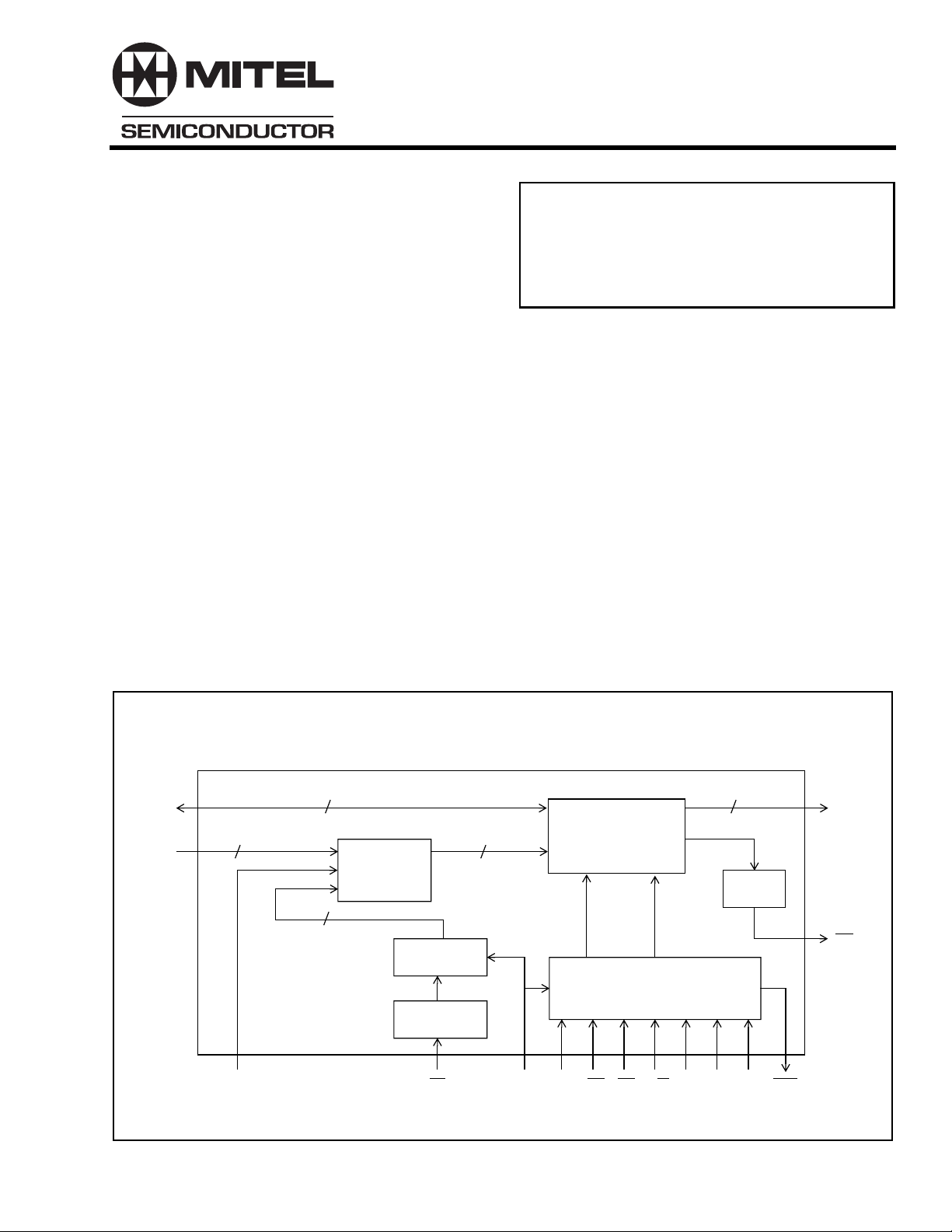
Figure 1 - Functional Block Diagram
2048 x 16
Static
Memory
WR
ENABLE
Control Interface
PRECHARGE
16
CRC
D0o/
D15o
CD
2-101
MT9080B CMOS
D8i
D9i
D10i
D11i
VSS
D12i
D13i
D14i
D15i
VSS
CK
VDD
VSS
IC
IC
FP
CS
DS
R/W
DTA
NC
VSS
D7i
D6i
D5i
D4i
VSS
D3i
D2i
D1i
VSS
VDD
D15o
D14o
D13o
D12o
VSS
D11o
D10o
D9o
D0i
8
6
4
12
10
14
16
18
20
22
24
26
28
30
32
34
36
38
MxMyMz
NC
ME
VSS
ODE
2
84
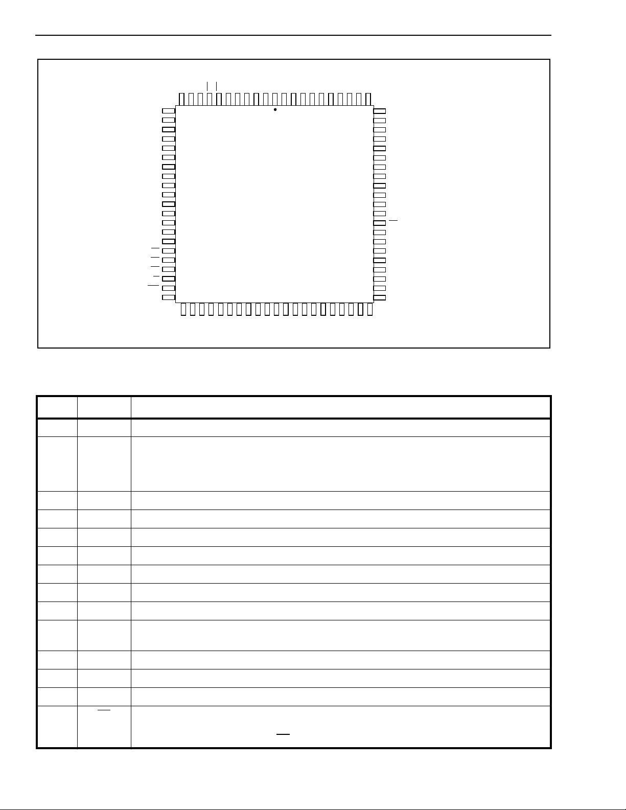
84 PIN PLCC
40
NC
44
42
IC
IC
NC
VSS
VDD
82
80
46
48
A0A1A2A3A4A5A6
D8o
78
50
VSS
76
74
D7o
D6o
72
D5o
D4o
70
VSS
D3o
68
D2o
D1o
66
D0o
VSS
64
VDD
62
CD
A15
60
A14
A13
58
A12
A11
56
A10
A9
A8
54
52
A7
Figure 2 - Pin Connections
Pin Description
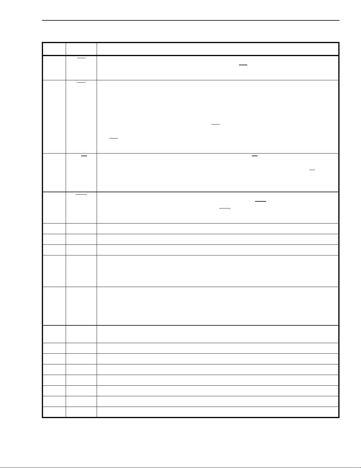
Pin # Name Description
1VSSGround.
2-5 D0i-D3i Input/Microport Data Bus. This is part of a 16 bit data bus. The data bus is bidirectional in
Connect Memory mode where it is typically interfaced to a microprocessor. In all other
modes the data bus is an input. Data to be switched through the device is clocked in at this
port.
6VSSGround.
7-10 D4i-D7i Input/Microport Data Bus. See description for pins 2-5 above.
11 V
SS
12-15 D8i-D11i Input/Microport Data Bus. See description for pins 2-5 above.
16 V
SS
17-20 D12i-D15i Input/Microport Data Bus. See description for pins 2-5 above.
21 V
SS
22 CK Clock. Master clock input which is used to clock data into and out of the de vice. It also cloc ks
Ground.
Ground.
Ground.
the internal 11 bit counter.
23 V
24 V
DD
SS
+5V supply input.
Ground.
25,26 IC Internal Connection. Should be tied to VSS for normal operation.
27 FP Frame Pulse. An active low signal that serves as a synchronous clear for the internal 11 bit
counter in all modes except Shift Register mode. The counter is cleared on a rising edge of
CK. In the Shift Register mode, FP serves to align channel boundaries.
2-102
CMOS MT9080B
Pin Description
Pin # Name Description
28 CS Chip Select. Active Low input. Selects the device for microport access in connect memory,
data memory, external and shift register modes. Tying CS high will disable output data
drivers (D0-D15o) in all modes except connect memory and shift register modes.
29 DS Data Strobe. Active low input. Indicates to the SMX that valid data is present on the
microport data bus during a write operation or that the SMX must output data on a read
operation.
In Connect Memory modes, a low level applied to this input during a write operation indicates
to the SMX that valid data is present on the microport data bus. During a read operation the
low going signal indicates to the SMX that it must output data on the microport data bus.
In Data Memory and External modes, when DS is high, the output data bus D0o-D15o will be
disabled. The input data bus D0i-D15i is not affected.
The DS input has no effect on the input and output busses in Counter or Shift Register
modes.
30 R/W Read/Write Enable. Data is written into the device when R/W is low and read from it when it
is high. This control input is disabled in data memory and shift register modes. It should be
tied to VSS or VDD in these modes. In counter and external modes, the state of R/W pin is
clocked in with the rising edge of CK. The actual read or write operation will be implemented
on the next rising clock edge.
31 DTA Data Transfer Acknowledge. Open drain output which is pulled low to acknowledge
completion of microport data transfer. On a read of the SMX,DT A low indicates that the SMX
has put valid data on the data bus. On a write, DTA low indicates that the SMX has
completed latching the data in.
32 NC No Connection.
33 V
SS
Ground.
34 NC No Connection.
35 ODE Output Data Enab le. Control input which enab les the output data bus. Pulling this input low
will place the data bus in a high impedance state. The level on this pin is latched by a rising
edge of CK. The output drivers will be enabled or disabled with the rising edge in the next
timeslot (see Fig. 24 for applicable timing in different modes).
36 ME Message Enable. When tied high the data latched in on the address bus is clocked out on
D0o-D15o. When ME is tied low, the contents of the addressed memory location will be
output on the bus. The level on this pin is latched in with the rising edge of the clock. The
actual mode change is implemented on the rising edge in the next timeslot. Refer to Figures
25 and 26 for more timing information.
37 Mx Mode X. One of three inputs which permit the selection of different operating modes for the
device. Refer to Table 1 for description of various modes.
38 My Mode Y. See description for pin 37.
39 Mz Mode Z. See description for pin 37.
40 NC No Connection.
41, 42 IC Internal Connection. Leave open for normal operation.
43 V
44 V
SS
DD
Ground.
Supply Voltage. +5V.
45 NC No Connection.
2-103

MT9080B CMOS
Pin Description
Pin # Name Description
46-61 A0-A15 Address Bus. These inputs have three different functions. Inputs A0-A10 are used to
address internal memory locations during read or write operations in all modes except Shift
Register mode. In Shift Register mode, the levels latched in on A0-A10 program the delay
through the device. When the ME pin is tied high, the data latched in on A0-A15 is clocked
out on to the data bus (D0o-D15o).
62 CD Change Detect. Open drain output which is pulled low when a change in the memory
contents from one frame to the next is detected by a Cyclic Redundancy Check (CRC).
Changes in memory contents resulting from microprocessor access do not cause CD to go
low. The output is reset to its normal high impedance state when the DS input is strobed,
while the device has been selected (CS is low).
63 V
64 V
DD
SS
Supply Voltage. +5V.
Ground.
65-68 D0o-D3o Output Data Bus. These three state outputs are part of a 16 bit data bus which is used to
clock out data from the device. Data is clocked out with the rising edge of the clock. See
Figures 24 to 26 for timing information. The bus is activ ely driven when ODE is tied high. It is
disabled when ODE is tied low. Tying CS high will also disable the output data bus in all
modes except Connect Memory and Shift Register Modes.
69 V
SS
Ground.
70-73 D4o-D7o Output Data Bus. See description for pins 65-68.
74 V
SS
Ground.
75-78 D8o-D11o Output Data Bus. See description for pins 65-68.
79 V
SS
Ground.
80-83 D12o-D15oOutput Data Bus. See description for pins 65-68.
84 V
DD
Supply Voltage. +5V.
2-104
CMOS MT9080B
Functional Description
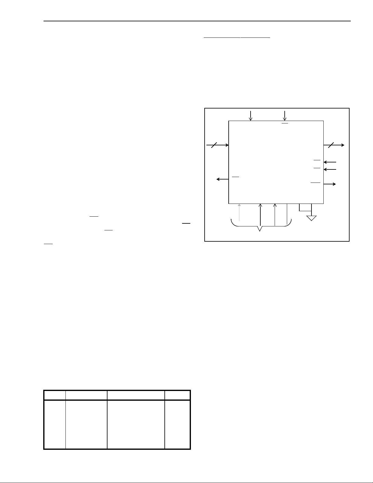
The SMX is a flexible memory module suitable for
use in the construction of timeslot interchange
circuits used in PCM voice or data switches. The
device can be configured as a data memory or a
connection memory.
The SMX has separate 16 bit input and output data
busses. A 16 bit address bus and a full
microprocessor interface is also provided.
Data is clocked into and out of the device with the
signal applied at the CK (clock) input. Depending on
the mode of operation, the memory locations for the
read or write operation can be addressed
sequentially by the internal counter or randomly via
the external address bus. A messaging sub-mode,
which permits the data latched in on the address bus
to be multiplexed on to the output data bus, is also
available (see ME pin description).
The SMX ensures integrity of the stored data by
performing a Cyclic Redundancy Check (CRC) on a
per frame basis. When a change in the memory
contents is detected from one frame to the next, the
Change Detect (CD) pin is pulled low. The output will
be reset to its normal high impedance state when DS
input is strobed while CS is low (i.e., while the device
has been selected for microprocessor access). The
CD output is not pulled low when the memory
contents have been modified by a processor access
to the device.
Modes Of Operation
The SMX can be programmed to operate in one of
eight modes as summarized in Table 1. The different
modes are used to realize specific switch
implementations. For example, to implement a 1024
channel switch, two SMXs are required. One is
operated in Data Memory mode, while the second is
operated in Connect Memory mode. A 2048 channel
switch can be realized using three SMXs. Two of the
devices are operated, alternatively, in Counter and
External modes, the third serves as the Connection
Memory. A detailed description of the
implementation is presented in the Applications
section of this data sheet. An outline of the device
functionality in each mode is presented below.
Mode MXMYM
1
0
2
0
3
0
4
0
5
1
6
1
7
1
8
1
Z
0
0
0
1
1
0
0
1
1
Data Memory - 1
1
Data Memory - 2
0
Connect Memory - 1
1
Connect Memory - 2
0
Counter Mode
1
External Mode
0
Shift Register Mode
1
Data Memory - 3
Table 1. SMX Modes of Operation
Name Abbr.
DM-1
DM-2
CM-1
CM-2
CNT
EXT
SR
DM-3
Data Memory Mode-1
Data Memory Mode-1 is designed for use in the
construction of a 1024 Channel Switch Matrix. Data
on the D0-D15 input bus is clocked into the SMX and
stored in memory locations addressed by the internal
11 bit counter. Data is clocked out according to the
addresses asserted on the address bus. The pin
configuration of the device in this mode is illustrated
in Figure 3
Data
Input
16
CK
-D15
D0
i
i
CD
A0-A15 ME ODE ZYZ
From Control Interface
FP
MODE
D0
-D15
o
CS
DS
DTA
o
Data
Output
16
Figure 3 - Data Memory Modes 1 and 2 Pinout
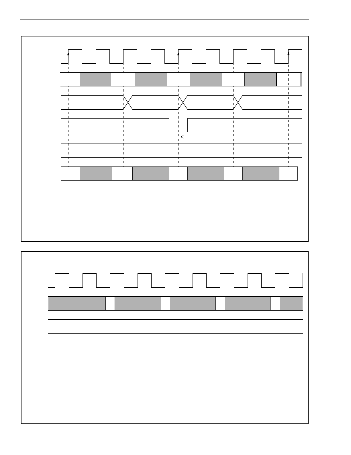
The timing for the read and write operation is
illustrated in Figure 4. The first half of each clock
period is used for precharging the internal bus. Data
is latched in and out of the device with rising edge of
the CK clock. Correct operation of the device in this
mode requires 2048 clock cycles in a single frame
defined by the frame pulse. Consequently, for
switching of 64 kbit/s PCM voice channels, the clock
frequency must be 16.384 Mbit/s with a frame rate of
8 kHz.
The address supplied on the address bus is latched
in with the first positive clock edge in a channel
timeslot. The contents of the memory location
addressed will be clocked out on D0-D15o with the
first positive clock edge in the next timeslot (see
Figure 4).
In Data Memory Mode-1, the delay through the
switch depends on the number of channel timeslots
between the input channel and the output channel. If
the time difference between the input channel and
output channel is less than two channels, data
clocked into the device in the current frame will be
clocked out in the next frame. If the difference is
greater than or equal to two channels, data will be
clocked out in the same frame. This concept is
further illustrated in Figure 5.
2-105
MT9080B CMOS
➀②
CK
External
Address
Bus A0-A15
Data Output
D0-D15o
FP
Address
generated by
Internal 11
Bit Counter
Data Input
D0-D15i
Data is clocked out of the memory location addressed by external address bus. The address is latched in with CK edge
marked ➀. Data is clocked out with CK edge marked②.
CH X CH Y CH Z
1022
PWP R
CH X CH Y CH Z
1023
P = Precharge
R = Read Memory
W = Write Memory
Counter Reset
0
➂➃
1
2101023
CK
Input
Data
Output
Timeslots
Data is latched into the device with the last rising edge of CK in the timeslot (e.g., edge ➂ in diagram). It is stored in the
memory location address by the internal 11 bit counter with the next rising clock edge (edge ➃ in diagram).
Figure 4 - Data Memory Mode Functional Timing
➀②
PW R
1 4
12345
Data on the input bus of the SMX is latched into the device with last rising edge of the clock within a timeslot. It is
written into the internal memory with the following positive edge.
Data is clocked out of the memory location and latched onto the output data bus with first positive clock edge in the
timeslot.
Switching channel 1 to channel 1 or channel 2 will result in one frame delay. Note that channel 2 is clocked out by CK
edge labelled ➀ while channel 1 is written into the memory with edge②. However, if channel 1 is switched to channel
3, there will be only one channel delay.
P
2 3
P = Precharge
R = Read Memory
W = Write Memory
2-106
Figure 5 - Throughput Delay in Data Memory Mode-1
CMOS MT9080B
This mode provides minimum delay through the SMX
for any switching configuration.
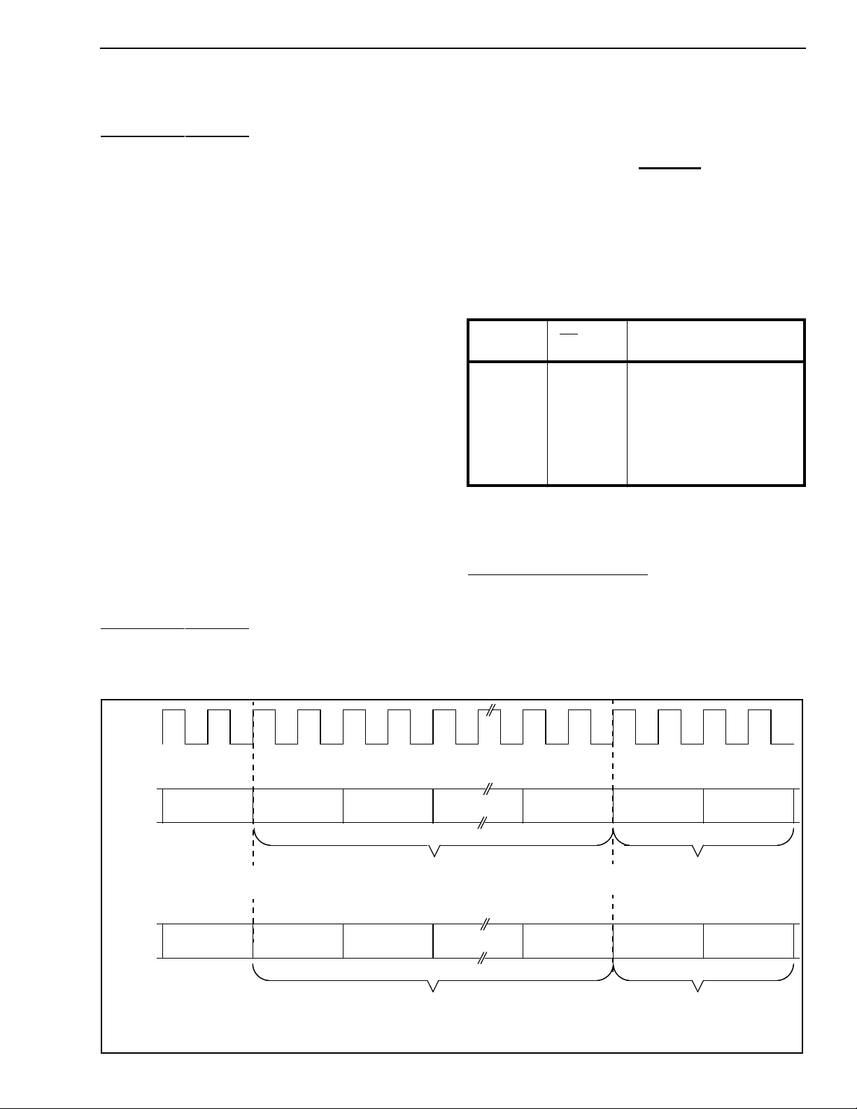
Data Memory Mode-2
Data Memory Mode-2 is designed for use in
constructing a 1024 by 1024 channel double buff ered
switch. This mode is similar in most respects to Data
Memory Mode-1. The double buffering is achiev ed by
dividing the internal 2048 memory into two equal
blocks. In a single frame, data is written into the first
block and read from the second. In the next frame,
the data will be written into the second and read from
the first (see Figure 6). Frame sequence integrity of
the data will be maintained for all switching
configurations if the output frame is delayed by one
channel with respect to the input frame. In this case,
data clocked into the device during any of the
channels in the current frame will be clocked out in
the next frame. However, if the input and output
frames are aligned, then data switched from any
input channel to output channels 0 or 1 will be
clocked out one frame after the next - consequently
frame sequence integrity is not maintained for
channels 0 or 1. Frame sequence integrity will be
maintained for data switched to any of the other
output channels. (See SMX/PAC Application Note,
MSAN-135, for more information.)
acceptable clock frequency or frame rate. In this
mode, the size of the switching matrix depends on
the clock and frame rates provided as per the
following relationship:
F
=
CK
2 X F
FP
S
where S is the number of channels in the switching
matrix FFP is the frame pulse frequency in Hz, and
FCK is the clock frequency in Hz. The following table
shows how the size of a switching matrix can be
varied by selecting a suitable combination of clock
and frame rates.
CK (MHz) FP (kHz)
16.384
16.384
16.384
12.288
12.288
8.192
8.192
4
8
16
4
8
4
8
Number of channels in
the switching matrix
2,048
1,024
512
1,536
768
1,024
512
It is not possible to switch between Data Memory
Mode-3 and other modes on per-timeslot basis.
It is possible to switch between Data Memory
Mode-1 and Mode-2 on a per timeslot basis.
Data Memory Mode-3
This mode is similar to Data Memory Mode-1.
However, there is no restriction on the minimum
CK
FRAME 1
1
Written to Block 0 Written to Block 1
FRAME 1
Data
Input
Data
Output
FRAME 0
1023
Written to
Block 1
FRAME 0
1023
0
Connect Memory Mode -1
In Connect Memory Mode-1, the input data bus is
bidirectional. Internal memory locations can be
randomly accessed via the microprocessor bus. The
pinout of the device in this mode is illustrated in
Figure 7.
FRAME 2
1023
102301 01
0
1
FRAME 2
Read from
Block 0
Note: No input and output channel alignment is implied in the example shown above. It is assumed that the frame pulse for the
connection memory used to generate adresses for the read operation has a specific phase relationship with respect to the Data
Memory frame pulse.
Read from Block 1 Read from Block 0
Figure 6 - Data Memory Mode-2 Functional Timing
2-107
MT9080B CMOS
Connect Memory Mode-2
16
Microprocessor
Interface
CK
D0-D15
A0-A15
CS
DS
W
R/
DTA
CD
ME Z Y X
FP
D0o-D15
MODE
0/1 1 0
16
o
ODE
Figure 7 - Connect Memory Modes Pinout
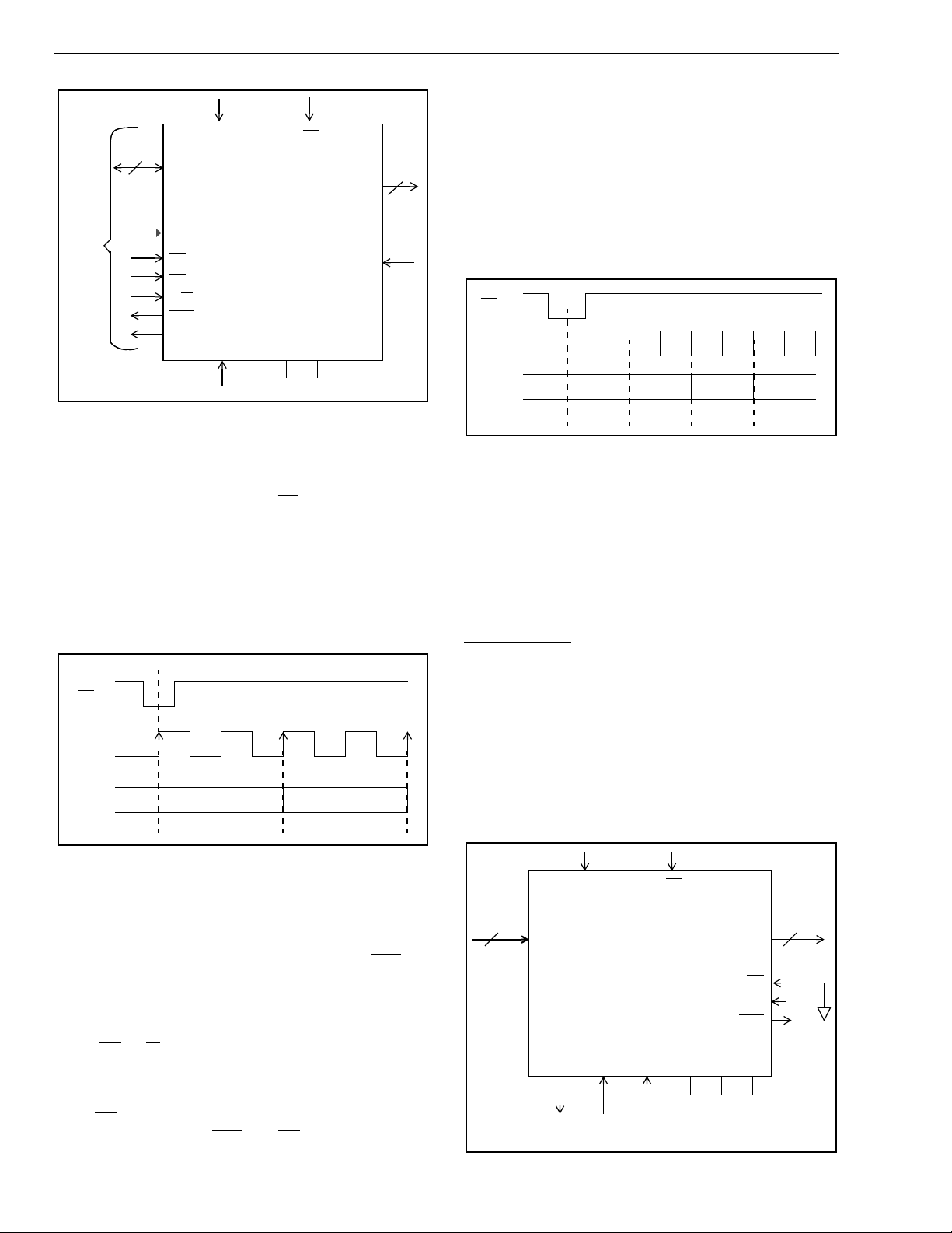
Data is clocked out on D0o-D15o from memory
locations addressed sequentially by the internal
counter. This counter is incremented every second
clock period and is reset with FP. The frequency of
the clock signal used should be twice the data rate.
A timing diagram showing the relationship between
the data output and the clock signal is presented in
Figure. 8. With a clock rate of 16.384 MHz, the
maximum number of addresses that can be
generated in an 8 kHz frame period is 1024.
Connect Memory Mode-2 is designed specifically for
2048 channel switching applications. Data is clocked
out on D0o-D15o with every rising clock edge from
memory locations addressed sequentially by the
internal counter (see Figure 9). This counter is
incremented with each clock period and is reset with
FP or when a count of 2047 is reached.
FP
CK
DATA
OUTPUT
2047 0 1 2
Fig. 9 - Connect Memory Mode-2 Functional
Timing
The clock frequency should be 16.384 MHz for a
connection memory designed to support a 2048
channel switch.
Microprocessor access is similar to Connect Memory
Mode-1.
Counter Mode
FP
CK
Data
Out
1023 0
Fig. 8 - Connect Memory Mode-1 Functional
Timing
Microprocessor access timing is shown in Figures 28
and 29. During a microprocessor read cycle, DS low
indicates to the SMX that the processor is ready to
receive data. The SMX responds by pulling DTA low
when there is valid data present on the bus. The
processor latches the data in and sets DS high. The
SMX completes the bus cycle by disabling the DTA.
DS should be kept low until afterDT A is issued by the
SMX. CS, R/W and the address lines should also be
asserted for the duration of the access. A MPU write
cycle is similar to the read cycle. Data will be latched
into the device approximately three clock (CK) cycles
after DS goes low. When the device has latched
the data in, it will pull DTA low. DS can subsequently
be set high.
This mode is designed for 2048 channel switching
applications. In the counter mode all read and write
addresses are generated sequentially by the internal
11 bit counter. The 11 bit counter is incremented with
each clock pulse. It will wrap around when it reaches
a count of binary 2047 or when it is reset by FP. The
active input/output pins in this mode are illustrated in
Figure 10.
16
CK
-D15
D0
i
i
CD R/WMEXYZ
FP
D0o-D15
ODE
DTA
100
All other inputs should
be tied Low
CS
o
16
Fig. 10 - Counter Mode Pinout
2-108
 Loading...