MITEL MT9076AB, MT9076AP Datasheet
MT9076
T1/E1/J1 3.3V Single Chip Transceiver
Preliminary Information
Features
• Combined T1/E1/J1 framer and LIU, with PLL
and 3 HDLCs
• In T1/J1 mode the LIU can recover signals
attenuated by up to 43dB (7000ft of 22 AWG
cable)
• In E1 mode the LIU can recover signals
attenuated by up to 43dB (2200m of 0.65mm
cable)
• Low jitter digital PLL (intrinsic jitter < 0.02UI)
• HDLCs can be assigned to any timeslot
• Comprehensive alarm detection, performance
monitoring and error insertion functions
• 2.048Mbit/s or 8.192Mbit/s ST-BUS streams
• Support for Inverse Mux for ATM (IMA)
• Support for V5.1 and V5.2 Access Networks
• 3.3V operation with 5V tolerant inputs
• Intel or Motorola non-multiplexed 8-bit
microprocessor port
• JTAG boundary scan
Applications
• E1/T1 add/drop multiplexers
• Access networks
• Primary rate ISDN nodes
• Digital Cross-connect Systems (DCS)
DS5289 ISSUE 1 January 2000
Ordering Information
MT9076AP 68 Pin PLCC
MT9076AB 80 Pin LQFP
-40 to +85°C
Description
The MT9076 is a highly featured single chip solution
for terminating T1/E1/J1 trunks. It contains a longhaul LIU, an advanced framer, a high performance
PLL, and 3 HDLCs.
In T1 mode, the MT9076 supports D4, ESF and
SLC-96 formats meeting the latest recommendations
including AT&T PUB43801, TR-62411; ANSI T1.102,
T1.403 and T1.408; Telcordia GR-303-CORE.
In E1 mode, the MT9076 supports the latest ITU-T
Recommendations including G.703, G.704, G.706,
G.732, G.775, G.796, G.823, G.964 (V5.1), G.965
(V5.2) and I.431. It also supports ETSI ETS 300 011,
ETS 300 166, ETS 300 233, ETS 300 324 (V5.1) and
ETS 300 347 (V5.2).
DSTi
CSTi
Tdi
Tdo
Tms
Tclk
Trst
IRQ
D7~D0
AC4
AC0
R/W/WR
CS
DS/RD
DSTo
CSTo
ST-BUS
Interface
ST Loop
IEEE
1149.1
Interface
Microprocessor
ST-BUS
Interface
RxDLCLK RxDL
TxDL TxDLCLK
Data Link,
HDLC0
HDLC1
Alarm Detection, 2 Frame Slip Buffer
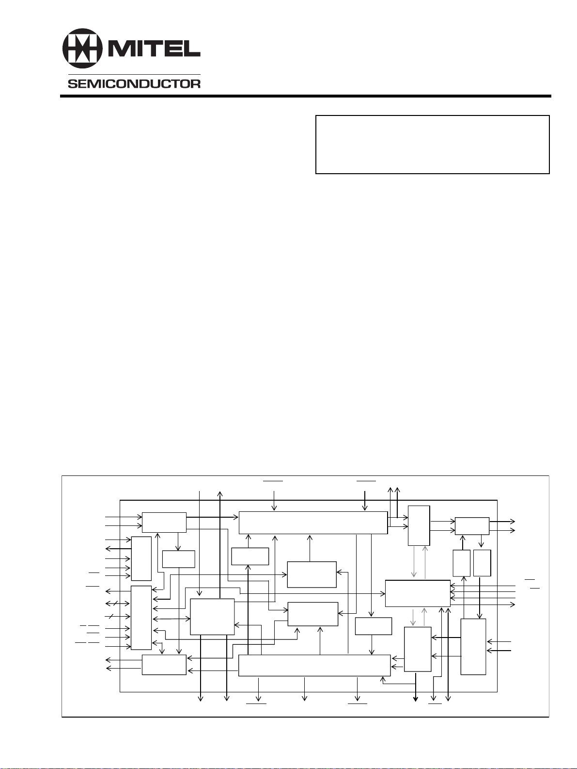
Figure 1 - MT9076 Functional Block
TxMF
Transmit Framing, Error,
Test Signal Generation and Slip Buffer
PL Loop
National
Bit Buffer
CAS
Buffer
Receive Framing, Performance Monitoring,
TxAO TxB TxA
DG Loop
RxFP
Pulse
Generator
Jitter Attenuator
& Clock Control
Recovery
Clock,Data
Exclk
F0b C4bRxMF/TxFP LOS
Line
Driver
RM
Loop
MT
Rx Equalizer
& Data Slicer
Loop
TTIP
TRING
S/FR
BS/LS
OSC1
OSC2
RTIP
RRING
1
MT9076 Preliminary Information
FR/Exclki
DS/RD
DSTi
CSTi
DSTo
CSTo
VDD4
VSS4
OSC2
OSC1
VSS3
S/
VDD3
TxDLCK
TxDL
IC3
IC2
LOS
RESET
INT/
VDD5
R/
INT/
R/
NC
NC
CS
IRQ
D0
D1
D2
D3
VSS5
IC4
MOT
D4
D5
D6
D7
W/WR
AC0
NC
CS
RESET
IRQ
D0
D1
D2
D3
VSS5
IC4
MOT
VDD5
D4
D5
D6
D7
W/WR
AC0
8 6 4 2 68 66 64 62
10
12
14
16
AC3
CSTi
AC4
GNDARx
CSTo
68 PIN PLCC
RTIP
VDD1
RRING
VDDArx
VSS3
OSC1
OSC2
VSS4
VDD4
80 PIN LQFP
TXA
VSS1
VDD3
TXB
RxDCLK
FR/Exclki
TXDL
S/
18
20
22
24
26
28 30 32 34 36 38 40 42
AC1
AC2
NC
DS/RD
DSTo
DSTi
62
64
66
68
70
72
74
76
78
80
RxDL
TxMF
RxMF/TxFP
IC3
IC2
TCDLCK
60
58
56
54
52
50
48
46
44
LS
BS/
LOS
42444648505254565860
NC
NC
2018161412108642
TxAO
Trst
Tclk
Tms
Tdo
Tdi
GNDATX
TRING
TTIP
VDDATX
VDD2
VSS2
IC1
RxFP
F0b
C4b
Exclk
40
38
36
34
32
30
28
26
24
22
NC
NC
TxAO
Trst
Tclk
Tms
Tdo
Tdi
GNDATX
TRING
TTIP
VDDATX
VDD2
VSS2
IC1
RxFP
F0b
C4b
Exclk
NC
NC
AC1
AC3
AC2
AC4
RTIP
RRING
VDARx
GNDARx
VSS1
VDD1
TXA
TXB
RXDLCK
TxMF
RXDL
NC
BS/LS
RxMF/TxFP
NC
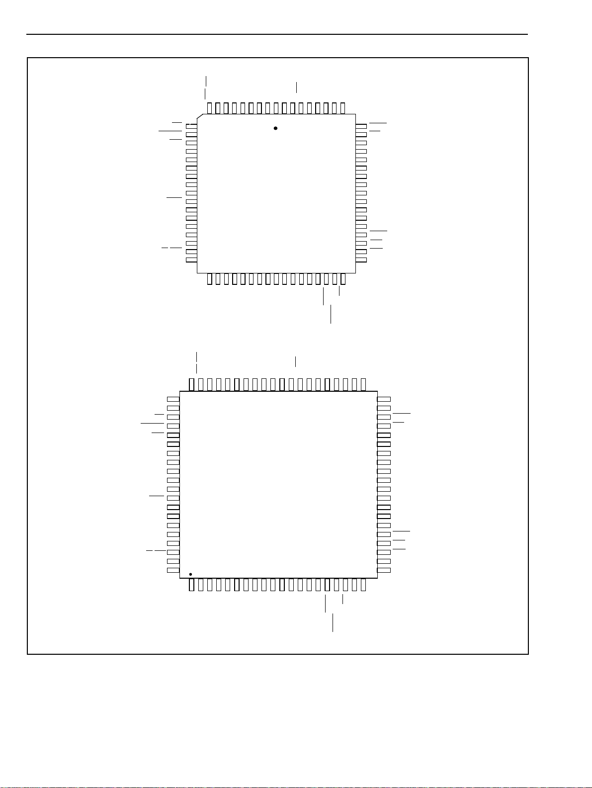
Figure 2 - Pin Connections
2
Preliminary Information MT9076
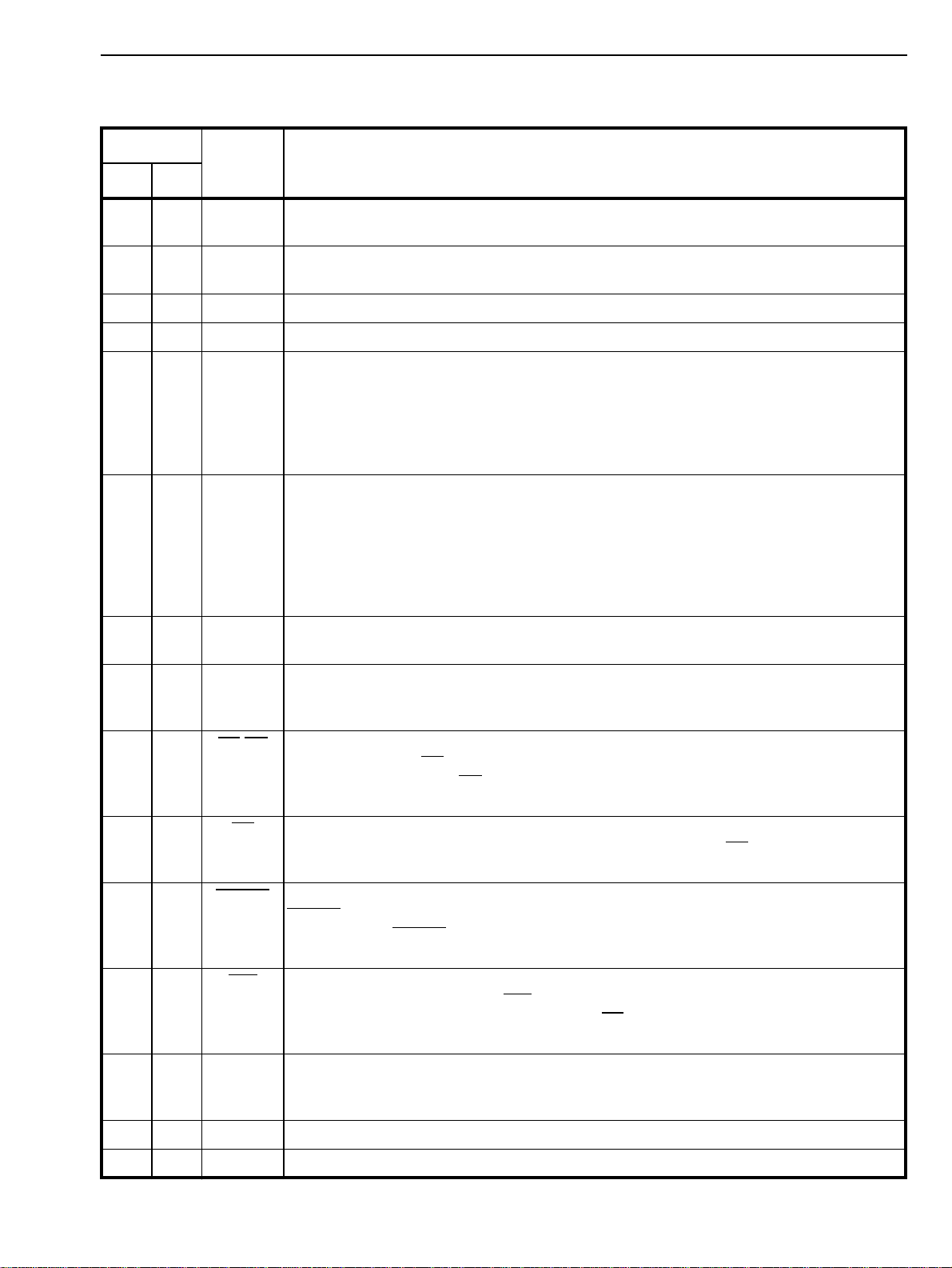
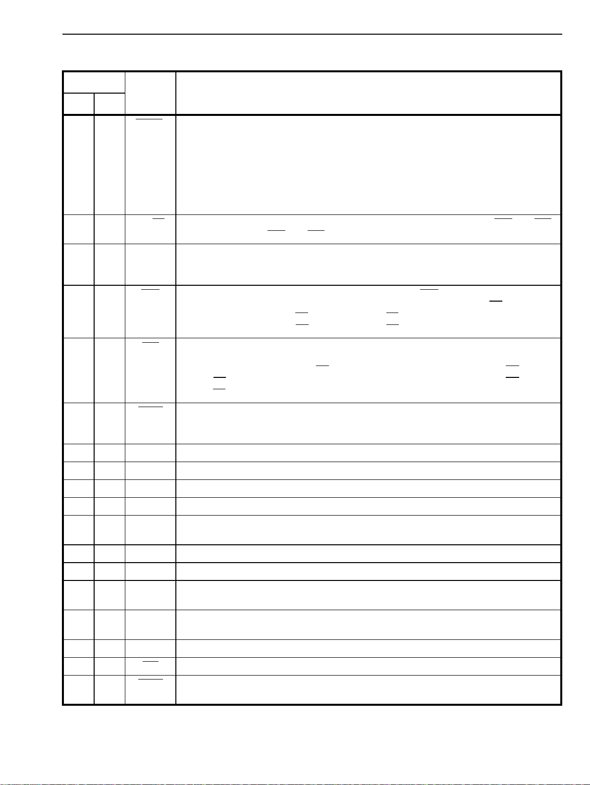
Pin Description
Pin #
Name Description
PLCC LQFP
1 51 OSC1 Oscillator (3V Input). This pin is either connected via a 20.000 MHz crystal to OSC2
where a crystal is used, or is directly driven when a 20.000 MHz. oscillator is employed.
2 52 OSC2 Oscillator (3V Output). Connect a 20.0 MHz crystal between OSC1 and OSC2. Not
suitable for driving other devices.
353V
454V
5 55 CSTo Control ST-BUS (5V tolerant Output). CSTo carries serial streams for CAS and CCS
6 56 CSTi Control ST-BUS (5V tolerant Input). CSTi carries serial streams for CAS and CCS
7 57 DSTo Data ST-BUS (5V tolerant Output). A 2.048 Mbit/s serial stream which contains the
8 58 DSTi Data ST-BUS (5V tolerant Input). A 2.048 Mbit/s serial stream which contains the
959DS/RD Data/Read Strobe (5V tolerant Input).
SS4
DD4
Negative Power Supply . Digital ground.
Positive Power Supply . Digital supply (+3.3V ± 5%).
respectively a 2.048 Mbit/s ST-BUS status stream which contains the 30 receive
signaling nibbles (ABCDZZZZ or ZZZZABCD). The most significant nibbles of each ST-
BUS time slot are valid and the least significant nibbles of each ST-BUS time slot are
tristated when control bit MSN (page 01H, address 1AH, bit 1) is set to 1. If MSN=0, the
position of the valid and tristated nibbles are reversed.
respectively a 2.048 Mbit/s ST-BUS control stream which contains the 30 transmit
signaling nibbles (ABCDXXXX or XXXXABCD) when RPSIG=0. When RPSIG=1 this
pin has no function. The most significant nibbles of each ST-BUS time slot are valid and
the least significant nibbles of each ST-BUS time slot are ignored when control bit MSN
(page 01H, address 1AH, bit 1) is set to 1. If MSN=0, the position of the valid and
ignored nibbles is reversed.
24/30 PCM(T1/E1) or data channels received on the PCM 24/30 (T1/E1) line.
24/30 (T1/E1) PCM or data channels to be transmitted on the PCM 24/30 (T1/E1)
line.
In Motorola mode (DS), this input is the active low data strobe of the processor
interface. In Intel mode (RD), this input is the active low read strobe of the processor
interface.
10 63 CS Chip Select (5V tolerant Input). This active low input enables the non-multiplexed
parallel microprocessor interface of the MT9076. When CS is set to high, the
microprocessor interface is idle and all bus I/O pins will be in a high impedance state.
11 64 RESET RESET (5V tolerant Input). This active low input puts the MT9076 in a reset condition.
RESET should be set to high for normal operation. The MT9076 should be reset after
power-up. TheRESET pin must be held low for a minimum of 1µsec. to reset the device
properly .
12 65 IRQ Interrupt Request (5V tolerant Output). A low on this output pin indicates that an
interrupt request is presented. IRQ is an open drain output that should be connected to
VDD through a pull-up resistor. An active low CS signal is not required for this pin to
function.
13 -1666-69 D0 - D3 Data 0 to Data 3 (5V tolerant Three-state I/O). These signals combined with D4-D7
form the bidirectional data bus of the parallel processor interface (D0 is the least
significant bit).
17 70 VSS5 Negative Power Supply. Digital ground.
18 71 IC4 Internal Connection (3V Input). Tie to VSS (Ground) for normal operation.
3

MT9076 Preliminary Information
Pin Description (continued)
Pin #
Name Description
PLCC LQFP
19 72 INT/MOT Intel/Motorola Mode Selection (5V tolerant Input). A high on this pin configures the
processor interface for the Intel parallel non-multiplexed bus type. A low configures the
processor interface for the Motorola parallel non-multiplexed type.
20 73 VDD5 Positive Power Supply. Digital supply (+3.3V ± 5%).
21 -2474-77 D4 - D7 Data 4 to Data 7 (5V tolerant Three-state I/O). These signals combined with D0-D3
form the bidirectional data bus of the parallel processor interface (D7 is the most
significant bit).
25 78 R/W/WR Read/Write/Write Strobe (5V tolerant Input). In Motorola mode (R/W), this input
controls the direction of the data bus D[0:7] during a microprocessor access. When R/W
is high, the parallel processor is reading data from the MT9076. When low, the parallel
processor is writing data to the MT9076. For Intel mode (WR), this active low write
strobe configures the data bus lines as output.
26 -3079,
31 6 GNDARx Receive Analog Ground. Analog ground for the LIU receiver.
32
33
34 9 VDDARx Receive Analog Power Supply. Analog supply for the LIU receiver (+3.3V ± 5%).
35 10 VDD1 Positive Power Supply. Digital supply (+3.3V ± 5%).
36 11 VSS1 Negative Power Supply. Digital ground.
37 12 TxA Transmit A (5V tolerant Output). When the internal LIU is disabled (digital framer
38 13 TxB Transmit B (5V tolerant Output). When the internal LIU is disabled and control bit
39 14 RxDLCLK Data Link Clock (5V tolerant Output). A gapped clock signal derived from the
AC0 - AC4 Address/Control 0 to 4 (5V tolerant Inputs). Address and control inputs for the
2-5
7
8
RTIP
RRING
non-multiplexed parallel processor interface. AC0 is the least significant input.
Receive TIP and RING (3V Input). Differential inputs for the receive line signal - must
be transformer coupled (See Figure 6). In digital framer mode these pins accept digital
3 volt signals from a physical layer device. They may accept a split phase unipolar
signal (RTIP and RRING employed) or an NRZ signal (RTIP only used).
only mode), if control bit NRZ=1, an NRZ output data is clocked out on pin TxA with the
rising edge of Exclk (TxB has no function when NRZ format is selected). If NRZ=0, pins
TxA and TxB are a complementary pair of signals that output digital dual-rail data
clocked out with the rising edge of Exclk.
NRZ=0, pins TxA and TxB are a complementary pair of signals that output digital dualrail data clocked out with the rising edge of Exclk.
extracted line clock, available for an external device to clock in RxDL data (at 4, 8, 12,
16 or 20 kHz) on the rising edge.
40 15 RxDL Receive Data Link (5V tolerant Output). A serial bit stream containing received line
data after zero code suppression. This data is clocked out with the rising edge of Exclk.
41 16 TxMF Transmit Multiframe Boundary (5V tolerant Input). An active low input used to set
the transmit multiframe boundary (CAS or CRC multiframe). The MT9076 will generate
its own multiframe if this pin is held high. This input is usually pulled high for most
applications.
4
Preliminary Information MT9076
Pin Description (continued)
Pin #
Name Description
PLCC LQFP
42 17 RxMF/
TxFP
Receive Multiframe Boundary / Transmit Frame Boundary (5V tolerant Output). If
the control bit Tx8KEN (page 02H address 10H bit 2) is low, this negative output pulse
delimits the received multiframe boundary. The next frame output on the data stream
(DSTo) is basic frame zero on the T1 or PCM 30 link. In E1 mode this receive
multiframe signal can be related to either the receive CRC multiframe (page 01H,
address 17H, bit 6, MFSEL=1) or the receive signaling multiframe (MFSEL=0). If the
control bit Tx8KEN is set high, this positive output pulse delimits the frame boundary
(the first bit transmit in the frame) for the digital output stream on pins TXA and TXB.
43 18 BS/LS Bus/Line Syncronization Mode Selection (5V tolerant Input). If high, C4b and F0b
will be inputs; if low, C4b and F0b will be outputs.
44 22 Exclk 2.048 MHz in E1 mode or 1.544MHz in T1 mode, Extracted Clock (5V tolerant
Output). The clock extracted from the received signal and used internally to clock in
data received on RTIP and RRING.
45 23 C4b 4.096 MHz System Clock (5V tolerant Input/Output). C4b is the clock for the ST-BUS
sections and transmit serial PCM data of the MT9076. In the free-run (S/FR/Exclki=0) or
line synchronous mode (S/FR/Exclki=1 and BS/LS=0) this signal is an output, while in
bus synchronous mode (S/FR/Exclki=1 and BS/LS=1) this signal is an input clock.
46 24 F0b Frame Pulse (5V tolerant Input/Output). This is the ST-BUS frame synchronization
signal, which delimits the 32 channel frame of CSTi, CSTo, DSTi, DSTo and the
PCM30 link. In the free-run (S/FR/Exclki=0) or line synchronous mode (S/FR/Exclki=1
and BS/LS=0) this signal is an output, while in bus synchronous mode (S/FR/Exclki=1
and BS/LS=1) this signal is an input.
47 25 RxFP Receive Frame Pulse/Receive CCS Clock (5V tolerant Output). An 8kHz pulse
signal, which is low for one extracted clock period. This signal is synchronized to the
receive DS1 or PCM 30 basic frame boundary.
48 26 IC1 Internal Connection. Must be left open for normal operation.
49 27 V
50 28 V
SS2
DD2
51 29 VDD
525330
31
TTIP
TRING
54 32 GND
Negative Power Supply. Digital ground.
Positive Power Supply. Digital supply (+3.3V ± 5%).
Transmit Analog Power Supply. Analog supply for the LIU transmitter (+3.3V ±5%).
ATx
Transmit TIP and RING(Output). Differential outputs for the transmit line signal - must
be transformer coupled (See Figure 6).
Transmit Analog Ground . Analog ground for the LIU transmitter.
ATx
55 33 Tdi IEEE 1149.1a Test Data Input (3V Input). If not used, this pin should be pulled high.
56 34 Tdo IEEE 1149.1a Test Data Output (5V tolerant Output). If not used, this pin should be
left unconnected.
57 35 Tms IEEE 1149.1a Test Mode Selection (3V Input). If not used, this pin should be pulled
high.
58 36 Tclk IEEE 1149.1a Test Clock Signal (3V Input). If not used, this pin should be pulled high.
59 37 Trst IEEE 1149.1a Reset Signal (3V Input). If not used, this pin should be held low.
60 38 TxAO Transmit All Ones (Input). High - TTIP, TRING will transmit data normally. Low - TTIP,
TRING will transmit an all ones signal.
5

MT9076 Preliminary Information
Pin Description (continued)
Pin #
Name Description
PLCC LQFP
61 43 LOS Loss of Signal or Synchronization (5V tolerant Output). When high, and LOS/LOF
(page 01H address 19H bit 0) is zero, this signal indicates that the receiv e portion of the
MT9076 is either not detecting an incoming signal (bit LLOS on page 03H address 16H
is one) or is detecting a loss of basic frame alignment condition (bit TSYNC (T1), SYNC
(E1) on page 03H address 10H is one). If LOS/LOF=1, a high on this pin indicates a
loss of signal condition.
62 44 IC2 Internal Connection (3V Input). Tie to VSS (Ground) for normal operation.
63 45 IC3 Internal Connection (3V Input). Tie to VSS (Ground) for normal operation.
64 46 TxDLCLK Transmit Data Link Clock (5V tolerant Output). A gapped clock signal derived from a
gated 2.048 Mbit/s clock for transmit data link at 4, 8, 12, 16 or 20 kHz. The transmit
data link data (TxDL) is clocked in on the rising edge of TxDLCLK. TxDLCLK can also
be used to clock DL data out of an external serial controller.
65 47 TxDL Transmit Data Link (5V tolerant Input). An input serial stream of transmit data link
data at 4, 8, 12, 16 or 20 kbit/s.
66 48 S/FR/
Exclki
67 49 VDD3 Positive Power Supply. Digital supply (+3.3V ± 5%).
68 50 VSS3 Negative Power Supply. Digital ground.
Synchronization/ Freerun / Extracted Clock (5V tolerant Input). If low, and the
internal LIU is enabled, the MT9076 is in free run mode. Pins 45 C4b and 46 F0b are
outputs generating sytem clocks. Slips will occur in the receive slip buffer as a result of
any deviation between the MT9076's internal PLL (which is free - running) and the
frequency of the incoming line data. If high, and the internal LIU is enabled, the MT9076
is in Bus or Line Synchronization mode depending on the BS/LS pin. If the internal LIU
is disabled, in digital framer mode, this pin (Exclki) tak es an input cloc k 1.544Mhz (T1) /
2.048Mhz (E1) that clocks in the received digital data on pins RXA and RXB with its
rising edge.
Device Overview
The MT9076 is a T1/E1/J1 single chip transceiver that incorporates an advanced framer, a long-haul LIU (Line
Interface Unit), a low jitter PLL (Phase Locked Loop) and 3 HDLCs (High-level Data Link Controller). The T1,
E1 and J1 operating modes are selectable under software control.
Standards Compliance
In T1 mode, the MT9076 meets or supports the latest recommendations including Telcordia GR-303-CORE,
AT&T PUB43801, TR-62411, ANSI T1.102, T1.403 and T1.408. In T1 ESF mode the CRC-6 calculation and
yellow alarm can be configured to meet the requirements of a J1 interface.
In E1 mode, the MT9076 meets or supports the latest ITU-T Recommendations for PCM 30 and ISDN primary
rate including G.703, G.704, G.706, G.732, G.775, G.796, G.823, G.964 (V5.1), G.965 (V5,2) and I.431. It also
meets or supports ETSI ETS 300 011, ETS 300 166, ETS 300 233, ETS 300 324 (V5.1) and ETS 300 347
(V5.2).
Microprocessor Port
The MT9076 registers are accessible via an 8-bit parallel Motorola or Intel non-multiplexed microprocessor
interface.
6

Preliminary Information MT9076
LIU
The MT9076 LIU interfaces the digital framer functions to either the DS1 (T1 mode) or PCM 30 (E1 mode)
transformer-isolated four wire line.
In T1 mode, the LIU can pre-equalize the transmit signal to meet the T1.403 and T1.102 pulse templates after
attenuation by 0 - 655 feet of 22 AWG PIC cable, alternatively it can provide line build outs of 7.5dB, 15dB and
22.5dB. In T1 mode the receiver can recover signals attenuated by up to 43dB at 772kHz.
In E1 mode, the LIU transmits signals that meet the G.703 2.048 Mbit/s pulse template and the receiver can
recover signals attenuated by up to 43dB at 1024kHz.
Digitial Framer Only Mode
To accommodate some special applications, the MT9076 suppor ts a digital framer only mode that provides
direct access to the transmit and receive data in digital format, i.e. by-passing the analog LIU front-end. In
digital framer only mode, the MT9076 supports unipolar non-return to zero or bipolar return to zero data.
PLL and Slip Buffers
The MT9076 PLL attenuates jitter from 2.5 Hz with a roll-off of 20 dB/decade. The intrinsic jitter is less than
0.02 UI. The device can operate in one of three timing modes: System Bus Synchronous Mode, Line
Synchronous Mode, or Free-run Mode. In all three timing modes the low jitter output of the PLL provides timing
to the transmit side of the LIU.
In T1 mode, the receive and transmit paths both include two-frame slip buffers. The transmit slip buffer features
programmable delay and serves as a Jitter Attenuator (JA) FIFO and a rate converter between the ST-BUS and
the 1.544 Mbit/s T1 line rate.
In E1 mode, the receive path includes a two-frame slip buffer and the transmit path contains a 128 bit Jitter
Attenuator (JA) FIFO with programmable depth.
Interface to the System Backplane
On the system side the MT9076 framers can interface to a 2.048Mbit/s or 8.192Mbit/s ST-BUS backplane.
There is an asynchronous mode for Inverse MUX for ATM (IMA) applications, this enables the framer to
interface to a 1.544Mbit/s (T1) or 2.048Mbit/s (E1) serial bus with asynchronous transmit and receive timing.
Framing Modes
The MT9076 framers operate in termination mode or transparent mode. In the receive transparent mode, the
received line data is channelled to the DSTo pin with arbitrary frame alignment. In the transmit transparent
mode, no framing or signaling is imposed on the data transmitted from the DSTi pin onto the line.
In T1 mode, the framers operate in any of the following framing modes: D4, Extended Superframe (ESF) or
SLC-96.
In E1 mode, the framers run three framing algorithms: basic frame alignment, signaling multiframe alignment
and CRC-4 multiframe alignment. The Remote Alarm Indication (RAI) bit is automatically controlled by an
internal state machine.
7

MT9076 Preliminary Information
Access to the Maintenance Channel
The T1 ESF Facility Data Link (FDL) bits can be accessed in the following three ways: Through the data link
pins TxDL, RxDL, RxDLC and TxDLC; through internal registers for Bit Oriented Messages; through an
embedded HDLC.
In E1 mode, the Sa bits (bits 4-8 of the non-frame alignment signal) can be accessed in four ways: Through
data link pins TxDL, RxDL, RxDLC and TxDLC, through single byte transmit and receive registers; through five
byte transmit and receive national bit buffers; through an embedded HDLC.
Robbed Bit Signaling/Channel Associated Signaling
Robbed bit signaling and channel associated signaling information can be accessed two ways: Via the
microport; via the CSTi and CSTo pins. Signaling information is frozen upon loss of multiframe alignment.
In T1 mode, the MT9076 supports AB and ABCD robbed bit signaling. Robbed bit signaling can be enabled on
a channel by channel basis.
In E1 mode the MT9076 supports Channel Associated Signaling (CAS) multiframing.
HDLCs
The MT9076 provides three embedded HDLCs with 128 byte deep transmit and receive FIFOs.
In T1 mode, the embedded HDLCs can be assigned to any channel and can operate at 56 kbit/s or 64 kbit/s. In
T1 ESF mode, HDLCO can be assigned to the 4 kbit/s FDL.
In E1 mode, the embedded HDLCs can be assigned to any timeslot and can operate at 64kbit/s. HDLCO can
be assigned to timeslot 0 Sa bits (bits 4-8 of the non-frame alignment signal) and can operate at 4,8,12,16 or
20kbit/s.
Performance Monitoring and Debugging
The MT9076 has a comprehensive suite of performance monitoring and debugging features. These include
error counters, loopbacks, deliberate error insertion and a 215 –1 QRS/PRBS generator/detector.
Interrupts
The MT9076 provides a comprehensive set of maskable interrupts. Interrupt sources consist of
synchronization status, alarm status, counter indication and overflow, timer status, slip indication, maintenance
functions and receive signaling bit changes.
8

Preliminary Information MT9076
MT9076 Detailed Feature List
Standards Compliance and Support
T1/J1 Mode E1 Mode
ANSI:
T1.102,T1.231, T1.403, T1.408
AT&T:
TR 62411, PUB43801
Telcordia:
GR-303-CORE
TTC:
JT-G703, JT-G704, JT-G706
Line Interface Unit (LIU)
• T1 and E1 modes use the same 1:2.4 transmit and receive transformers
• Internal register allows termination imepedance to be changed under software control.
• Programmable pulse shapes and pulse amplitudes
• Automatic or manual receiver equalization
• Receive signal peak amplitude is reported with 8-bit resolution
• Output pin to indicate Loss Of Signal/ Loss Of Frame synchronization
• LIU output is disabled at power-up until enabled by software
• Input pin to force transmission of AIS
ETSI:
ETS 300 011, ETS 300 166, ETS 300 233,
ETS 300 324, ETS 300 347
ITU:
G.703, G.704, G.706, G.732 G.775,
G.796, G.823, I.431, G.964, G.965
T1/J1 Mode E1 Mode
• Reliably recovers signals with cable
attenuation up to 43dB @ 772 kHz
• Transmit pulse meets T1.403 and T1.102
pulse templates
• Indicates analog Los Of Signal if the received
signal is more than 20 dB or 40dB below
nominal for more than 1ms
• Receiver tolerates jitter as required by AT&T
TR62411
• Transmit Pre-equalization and Line Build Out
options:
0-133 feet
133-266 feet
266-399 feet
399-533 feet
533-655 feet
-7.5dB
-15dB
-22.5dB
• Reliably recovers signals with cable
attenuation up to 43 dB @ 1024 kHz
• Transmit pulse meets G.703 pulse template
• Indicates analog Los Of Signal if the received
signal is more than 20dB or 40dB below
nominal for more than 1ms
• Receiver tolerates jitter as required by ETSI
ETS 300 011
9

MT9076 Preliminary Information
Digital Framer Mode
• The LIU can be disabled and bypassed to allow the MT9076 to be used as a digital framer
• Single phase NRZ or two phase NRZ modes are software selectable
• Line coding is software selectable
Phase Lock Loop
• Locks to a 4.096 MHz input clock, or to the 1.544MHz / 2.048MHz extracted clock
• IMA mode locks to 1,544MHz or 2,048MHz external clock
• Attenuates jitter from less than 2.5 Hz with a roll off of 20 dB/decade
• Attenuates jitter in the transmit or receive direction
• Intrinsic jitter less than 0.02 UI
• Meets the jitter characteristics as specified in AT&T TR62411
• Meets the jitter characteristics as specified in ETS 300 011
• Can be operated in Free-run, Line Synchronous or System Bus Synchronous modes
Access and Control
• MT9076 registers can be accessed via an 8-bit non-multiplexed parallel microprocessor port
• The parallel port can be configured for Motorola or Intel style control signals
Backplane Interfaces
• 2.048Mbit/s or 8.192Mbit/s ST-BUS
• IMA mode, 1.544Mbit/s (T1) or 2.048Mbit/s (E1) serial bus with asynchronous transmit and receive
timing for Inverse MUX for ATM (IMA) applications. Slip buffers are bypassed and signaling is disabled.
• CSTo/CSTi pins can be used to access the receive/transmit signaling data
• RxDL pin can be used to access the entire B8ZS/HDB3 decoded receive stream including framing bits
• TxDL pin can be used to transmit data on the FDL (T1) or the Sa bits (E1)
T1/J1 Mode E1 Mode
• PCM-24 channels 1-24 are mapped to STBUS channels 0-23 respectively
• The framing-bit is mapped to ST-BUS
channel 31
• PCM-30 timeslots 0-31 are mapped to STBUS channels 0-31 respectively
10

Preliminary Information MT9076
Data Link
T1/J1 Mode E1 Mode
• Three methods are provided to access the
datalink:
1. TxDL and RxDL pins support transmit and
receive datalinks
2. Bit Oriented Messages are supported via
internal registers
3. An internal HDLC can be assigned to transmit/
receive over the FDL in ESF mode
Access and Monitoring for National (Sa) Bits (E1 mode only)
• In addition to the datalink functions, the Sa bits can be accessed using:
• Single byte register
• Five byte transmit and receive national bit buffers
• A maskable interrupt is generated on the change of state of any Sa bit
Three Embedded Floating HDLCs (HDLC0, HDLC1, HDLC2)
• Successive writes/reads can be made to the transmit/receive FIFOs at 160 ns or 80ns intervals
• Flag generation and Frame Check Sequence (FCS) generation and detection, zero insertion and
deletion
• Continuous flags, or continuous 1s are transmitted between frames
• Transmit frame-abor t
• Transmit end-of-packet after a programmable number of bytes (up to 65,536 bytes)
• Invalid frame handling:
• Frames yielding an incorrect FCS are tagged as bad packets
• Frames with fewer than 25 bits are ignored
• Frames with fewer than 32 bits between flags are tagged as bad packets
• Frames interrupted by a Frame-Abort sequence remain in the FIFO and an interrupt is generated
• Access is provided to the receive FCS
• FCS generation can be inhibited for terminal adaptation
• Recognizes single byte, dual byte and all call addresses
• Independent, 16-128 byte deep transmit and receive FIFOs
• Receive FIFO maskable interrupts for near full (programmable levels) and overflow conditions
• Transmit FIFO maskable interrupts for nearly empty (programmable levels) and underflow conditions
• Maskable interrupts for transmit end-of-packet and receive end-of-packet
• Maskable interrupts for receive bad-frame (includes frame abort)
• Transmit-to-receive and receive-to-transmit loopbacks are provided
• Transmit and receive bit rates and enables are independent
• Frame aborts can be sent under software control and they are automatically transmitted in the event of
a transmit FIFO underrun
• Two methods are provided to access the
datalink:
1. TxDL and RxDL pins support transmit and
receive datalinks over the Sa4~Sa8 bits
2. An internal HDLC can be assigned to transmit/
receive data via the Sa4~Sa8 bits
• In transparent mode, if the Sa4 bit is used for
an intermediate datalink, the CRC-4
remainder can be updated to reflect changes
to the Sa4 bit
11

MT9076 Preliminary Information
T1/J1 Mode E1 Mode
HDLC0
• Assignable to the ESF Facility Data Link or
any channel
• Operates at 4 kbps, 56 kbps or 64 kbps
HDLC1, HDLC2
• Assignable to any channel
• Operates at 56 kbps or 64 kbps
Slip Buffers
T1/J1 Mode E1 Mode
Transmit Slip Buffer
• Two-frame slip buffer capable of performing a
controlled slip
• Intended for rate conversion and jitter
attenuation in the transmit direction
• Programmable delay • Indication of slip direction
• Transmit slips are independent of receive
slips
• Indication of slip direction
HDLC0
• Assigned to timeslot-0, bits Sa4~Sa8 or any
other timeslot
• Operates at 4, 8, 12, 16 or 20 kbps
depending on which Sa bits are selected for
HDLC0 use
HDLC1, HDLC
• Assigned to any timeslot except timeslot-0
• Operates at 64 kbps
Receive Slip Buffer
• Two-frame slip buffer capable of performing a
controlled slip
• Wander tolerance of 208 UI peak-to-peak
Receive Slip Buffer
• Two-frame slip buffer capable of performing a
controlled slip
• Wander tolerance of 142 UI (92 µs) peak
• Indication of slip direction
Jitter Attenuator FIFO
• A jitter attenuator FIFO is available on the transmit side in E1 mode and in IMA mode. The depth of the
JA FIFO can be configured to be from16 bits deep to 128 bits deep in 16 bit increments
Inverse Mux for ATM (IMA) Mode
T1/J1 Mode E1 Mode
• Transmit and receive datastreams are
independently timed
• The transmit clock synchronizes to a
1,544MHz clock
• Transmit and receive slip buffers are
bypassed
• Transmit and receive datastreams are
independently timed
• Receive slip buffer is bypassed
• CAS and HDLCs are disabled
• Robbed bit signaling and HDLCs are disabled
12

Preliminary Information MT9076
Framing Algorithm
T1/J1 Mode E1 Mode
• Synchronizes with D4 or ESF protocols
• Supports SLC-96 framing
• Framing circuit is off-line
• Transparent transmit and receive modes
• In D4 mode the Fs bits can optionally be
cross checked with the Ft bits
• The start of the ESF multiframe can be
determined by the following methods:
• Free-run
• Software reset
• Synchronized to the incoming multiframe
• An automatic reframe is initiated if the
framing bit error density exceeds the
programmed threshold
• In transparent mode, no reframing is forced
by the device
• Software can force a reframe at any time
• In ESF mode the CRC-6 bits can be
optionally confirmed before forcing a new
frame alignment
• During a reframe the signaling bits are frozen
and error counting for Ft, Fs, ESF framing
pattern and CRC-6 bits is suspended
• If J1 CRC-6 is selected the Fs bits are
included in the CRC-6 calculation
• J1 CRC-6 and J1 Yellow Alarm can be
independently selected
• Supports robbed bit signaling
• MT9076 contains 3 distinct and independent
framing algorithms
1. Basic frame alignment
2. Signaling multiframe alignment
3. CRC-4 multiframe alignment
• Transparent transmit and receive modes
• Automatic interworking between interfaces
with and without CRC-4 processing
capabilities is supported
• An automatic reframe is forced if 3
consecutive frame alignment patterns or
three consecutive non-frame alignment bits
are received in error
• In transparent mode, no reframing is forced
by the device
• Software can force a reframe at any time
• Software can force a multiframe reframe at
any time
• E-bits can optionally be set to zero until CRC
synchronization is achieved
• Optional automatic RAI
• Supports CAS multiframing
• Optional automatic Y-bit to indicate CAS
multiframe alignment
Line Coding
T1/J1 Mode E1 Mode
• B8ZS or AMI line coding
• Pulse density enforcement
• Forced ones insertion
• HDB3 or AMI line coding
13

MT9076 Preliminary Information
Channel Associated Signaling
• ABCD or AB bits can be automatically inserted and extracted
• Transmit ABCD or AB bits can be passed via the micropor t or via the CSTi pin
• Receive ABCD or AB bits are accessible via the microport or via the CSTo pin
• Most significant or least significant CSTi/CSTo nibbles can be selected to carr y signaling bits
• Unused nibble positions in the CSTi/CSTo bandwidth are tri-stated
• An interrupt is provided in the event of changes in any of the signaling bits
• Receive signaling bits are frozen if signaling multiframe alignment is lost
T1/J1 Mode E1 Mode
• Signaling bits can be debounced by 6 ms • Signaling bits can be debounced by14 ms
Alarms
T1/J1 Mode E1 Mode
D4 Yellow Alarm, two types
1. Bit position 2 is zero for virtually every DS0
over 48ms
2. Two consecutive ones in the S-bit position of
the twelfth frame
ESF Yellow Alarm, two types
1. Reception of 0000000011111111 in seven
or more codewords out of ten (T1)
2. Reception of 1111111111111111 in seven
or more codewords out of ten (J1)
Alarm Indication Signal (AIS)
• Declared if fewer than six zeros are detected
during a 3 ms interval
Loss Of Signal (LOS
• Analog Loss Of Signal is declared if the
received signal is more than 20 dB or 40 dB
below nominal for at least 1 ms
• Digital Loss Of Signal is declared if 192 or 32
consecutive zeros are received
• Output pin indicates LOS and/or loss of
frame alignment
)
Remote Alarm Indication (RAI)
• Bit 3 of the receive NFAS
Alarm Indication Signal (AIS
• Unframed all ones signal for at least a double
frame or two double frames
)
Timeslot 16 Alarm Indication Signal
• All ones signal in timeslot 16
Loss Of Signal (LOS)
• Analog Loss Of Signal is declared if the
received signal is more than 20 dB or 40 dB
below nominal for at least 1 ms
• Digital Loss Of Signal is declared if 192 or 32
consecutive zeros are received
• Output pin indicates LOS and/or loss of
frame alignment
Remote Signaling Multiframe Alarm
• Y-bit of the multiframe alignment signal
14

Preliminary Information MT9076
Maskable Interrupts
T1/J1 Mode E1 Mode HDLC Interrupts
• Change of state of terminal
synchronization
• Change of state of multiframe
synchronization
• Change of received bit
oriented message
• Change of state of reception
of AIS
• Change of state of reception
of LOS
• Reception of a severely
errored frame
• Transmit slip
• Receive slip
• Receive framing bit error
• Receive CRC-6 error
• Receive yellow alarm
• Change of receive frame
alignment
• Receive line code violation
• Receive PRBS error
• Pulse density violation
• Framing bit error counter
overflow
• CRC-6 error counter overflow
• Out of frame alignment
counter overflow
• Change of frame alignment
counter overflow
• Line code violation counter
overflow
• PRBS error counter overflow
• PRBS multiframe counter
overflow
• Multiframes out of alignment
counter overflow
• Loop code detected
• One second timer
• Five second timer
• Receive new bit oriented
message (debounced)
• Signaling (AB or ABCD) bit
change
• Change of state of basic
frame alignment
• Change of state of multiframe
synchronization
• Change of state of CRC-4
multiframe synchronization
• Change of state of reception
of AIS
• Change of state of reception
of LOS
• Reception of consecutively
errored FASs
• Receive remote signaling
multiframe alarm
• Receive slip
• Receive FAS error
• Receive CRC-4 error
• Receive E-bit
• Receive AIS in timeslot 16
• Line code violation
• Receive PRBS error
• Receive auxiliary pattern
• Receive RAI
• FAS error counter overflow
• CRC-4 error counter overflow
• Out of frame alignment
counter overflow
• Receive E-bit counter
overflow
• Line code violation counter
overflow
• PRBS error counter overflow
• PRBS multiframe counter
overflow
• Change of state of any Sa bit
or Sa nibble
• Jitter attenuator within 4 bits
of overflow/underflow
• One second timer
• Two second timer
• Signaling (CAS) bit change
• Go ahead pattern received
• End of packet received
• End of packet transmitted
• End of packet read from
receive FIFO
• Transmit FIFO low
• Frame abort received
• Transmit FIFO underr un
• Receive FIFO full
• Receive FIFO overflow
15

MT9076 Preliminary Information
Error Counters
• All counters can be preset or cleared under software control
• Maskable occurrence interrupt
• Maskable overflow interrupt
• Counters can be latched on one second intervals
T1/J1 Mode E1 Mode
• PRBS Error Counter (16-bit)
• CRC Multiframe Counter (16-bit)
• Framing Bit Error Counter (8-bit)
• Out of Frame Alignment Counter (4-bit)
• Change of Frame Alignment Counter (4-bit)
• Multiframes Out of Sync Counter (8-bit)
• Line Code Violation / Excessive Zeros
Counter (16-bit)
• CRC-6 Error Counter (16-bit)
Error Insertion
T1/J1 Mode E1 Mode
• Bipolar Violations
• CRC-6 Errors
• Ft Errors
• Fs Errors
• Payload Errors
• Loss of Signal Error
Loopbacks
• Errored FAS Counter (8-bit)
• E-bit Counter (10-bit)
• Line Code Violation / Excessive Zeros
Counter (16-bit)
• CRC-4 Error Counter (16-bit)
• PRBS Error Counter (8-bit)
• CRC Multiframe Counter (8-bit)
• Bipolar Violations
• CRC-4 Errors
• FAS Errors
• NFAS Errors
• Payload Errors
• Loss of Signal Error
• Digital loopback
• Remote loopback
• ST-BUS loopback
• Payload loopback
• Metallic loopback
• Local timeslot loopback
• Remote timeslot loopback
Per Timeslot Control
The following features can be controlled on a per timeslot basis:
• Clear Channel Capability (only used in T1/J1)
• Choice of sourcing transmit signaling bits from microport or CSTi pin
• Remote timeslot loopback
• Local timeslot loopback
• PRBS insertion and reception
• Digital milliwatt pattern insertion
• Per channel inversion
• Transmit message mode
16

MT9076
1.0 MT9076 Line Interface Unit (LIU)..................................................................................17
1.1 Receiver .................................................................................................................................................17
1.2 Transmitter .............................................................................................................................................18
1.3 20 Mhz Clock..........................................................................................................................................21
1.4 Phase Lock Loop (PLL)..........................................................................................................................22
2.0 Clock Jitter Attenuation Modes....................................................................................23
2.1 Jitter Attenuator FIFO.............................................................................................................................24
2.2 IMA Mode...............................................................................................................................................24
2.2.1 T1 Mode ......................................................................................................................................... 24
2.2.2 E1 Mode......................................................................................................................................... 24
3.0 The Digital Interface ......................................................................................................24
3.1 T1 Digital Interface .................................................................................................................................24
3.2 Frame and Superframe Structure in T1 mode........................................................................................25
3.2.1 Multiframing.................................................................................................................................... 25
3.3 E1 Digital Interface.................................................................................................................................27
3.3.1 Basic Frame Alignment .................................................................................................................. 28
3.3.2 CRC-4 Multiframing in E1 mode..................................................................................................... 29
3.3.3 CAS Signaling Multiframing in E1 mode......................................................................................... 30
4.0 MT9076 Access and Control.........................................................................................30
4.1 The Control Port Interface......................................................................................................................30
4.2 Control and Status Register Access.......................................................................................................31
4.3 Identification Code..................................................................................................................................31
4.4 ST-BUS Streams....................................................................................................................................31
5.0 Reset Operation (Initialization).....................................................................................32
6.0 Transmit Data All Ones (TxAO) Operation ..................................................................33
7.0 Data Link Operation ......................................................................................................33
7.1 Data Link Operation in E1 mode ............................................................................................................33
7.2 Data Link Operation in T1 mode ............................................................................................................33
7.2.1 External Data Link.......................................................................................................................... 35
7.2.2 Bit - Oriented Messaging................................................................................................................ 35
8.0 Floating HDLC Channels ..............................................................................................35
8.1 Channel Assignment ..............................................................................................................................35
8.2 HDLC Description...................................................................................................................................36
8.2.1 HDLC Frame structure ................................................................................................................... 36
8.2.2 Data Transparency (Zero Insertion/Deletion)................................................................................. 36
8.2.3 Invalid Frames................................................................................................................................ 36
8.2.4 Frame Abort.................................................................................................................................... 37
xvii

MT9076
8.2.5 Interframe Time Fill and Link Channel States ................................................................................ 37
8.2.6 Go-Ahead....................................................................................................................................... 37
8.3 HDLC Functional Description.................................................................................................................37
8.3.1 HDLC Transmitter........................................................................................................................... 37
8.3.2 HDLC Receiver............................................................................................................................... 38
9.0 Slip Buffers .................................................................................................................... 40
9.1 Slip Buffer in T1 Mode............................................................................................................................40
9.2 Slip Buffer in E1 mode............................................................................................................................42
10.0 Framing Algorithm ........................................................................................................ 43
10.1 Frame Alignment in T1 Mode.................................................................................................................43
10.2 Frame Alignment in E1 mode.................................................................................................................44
10.2.1 Notes for Synchronization State Diagram (Figure 16).................................................................... 46
10.3 Reframe..................................................................................................................................................46
10.3.1 E1 Mode........................................................................................................................................ 46
10.3.2 T1 Mode ......................................................................................................................................... 46
11.0 MT9076 Channel Signaling........................................................................................... 46
11.1 Channel Signaling in T1 Mode...............................................................................................................46
11.2 Channel Signaling in E1 Mode...............................................................................................................47
12.0 Loopbacks .....................................................................................................................48
13.0 Performance Monitoring............................................................................................... 49
13.1 Error Counters........................................................................................................................................49
13.2 T1 Counters............................................................................................................................................49
13.2.1 Framing Bit Error Counter (FC7-0)................................................................................................. 49
13.2.2 Out Of Frame / Change Of Frame Alignment Counter (OOF3-0/COFA3-0) .................................. 49
13.2.3 Multiframes out of Sync Counter (MFOOF7-MFOOF0).................................................................. 50
13.2.4 CRC-6 Error Counter (CC15-0)...................................................................................................... 50
13.2.5 Line Code Violation Error Counter (LCV15-LCV0)......................................................................... 50
13.2.6 PRBS Error Counter (PS7-0).......................................................................................................... 50
13.2.7 CRC Multiframe Counter for PRBS (PSM7-0)................................................................................ 50
13.3 E1 Counters ...........................................................................................................................................50
13.4 Errored FAS Counter (EFAS7-EFAS0)..................................................................................................50
13.5 E-bit Counter (EC15-0)...........................................................................................................................51
13.6 Line Code Violation Error Counter (LCV15-LCV0).................................................................................51
13.7 CRC-4 Error Counter (CC15-0)..............................................................................................................51
13.8 PRBS Error Counter (PS7-0) .................................................................................................................51
13.9 CRC Multiframe Counter for PRBS (PSM7-0)........................................................................................51
xviii

MT9076
14.0 Error Insertion................................................................................................................52
15.0 Per Time Slot Control Words........................................................................................52
15.1 Clear Channel Capability........................................................................................................................52
15.2 Microport signaling .................................................................................................................................52
15.3 Per Time Slot Looping............................................................................................................................52
15.4 PRBS Testing.........................................................................................................................................53
15.5 Digital Milliwatt........................................................................................................................................53
15.6 Per Channel Inversion............................................................................................................................53
15.7 Transmit Message..................................................................................................................................54
16.0 Alarms ............................................................................................................................54
16.1 Automatic Alarms ...................................................................................................................................54
17.0 Detected Events.............................................................................................................55
17.1 T1 mode .................................................................................................................................................55
17.1.1 Severely Errored Frame Event....................................................................................................... 55
17.1.2 Loop Code Detect........................................................................................................................... 55
17.1.3 Pulse Density Violation Detect ....................................................................................................... 55
17.1.4 Timer Outputs................................................................................................................................. 55
17.2 E1 mode.................................................................................................................................................55
17.2.1 Consecutive Frame Alignment Patterns (CONFAP)....................................................................... 55
17.2.2 Receive Frame Alignment Signals ................................................................................................. 55
17.2.3 Receive Non Frame Alignment Signal............................................................................................ 55
17.2.4 Receive Multiframe Alignment Signals........................................................................................... 55
18.0 Interrupts........................................................................................................................55
18.1 Interrupts on T1 Mode............................................................................................................................56
18.2 Interrupts on E1 Mode............................................................................................................................56
19.0 Digital Framer Mode......................................................................................................57
19.1 T1 Mode .................................................................................................................................................57
19.1.1 E1 mode......................................................................................................................................... 57
20.0 Control and Status Registers.......................................................................................58
20.1 T1 Mode .................................................................................................................................................58
20.1.1 Master Control 1 (Page 01H) (T1).................................................................................................. 58
20.1.2 Master Control 2 (Page 02H) (T1).................................................................................................. 69
20.1.3 Master Status 1 (Page03H) (T1) .................................................................................................... 75
20.1.4 Master Status 2 (Page04H) (T1).................................................................................................... 80
20.1.5 Per Channel Transmit signaling (Pages 5 and 6) (T1) 88
20.2 Per Time Slot Control Words (Pages 7 and 8) (T1) ...............................................................................90
20.2.1 Per Channel Receive signaling (T1 and E1 mode) (Pages 9 and 0AH)......................................... 91
20.3 E1 Mode.................................................................................................................................................92
xix

MT9076
20.3.1 Master Control 1 (Page 01H) (E1).................................................................................................. 92
20.4 Master Control 2 (Page-2)....................................................................................................................103
20.4.1 Master Control 2 (Page 02H) (E1)................................................................................................ 103
20.5 Master Status 1 (Page03H) (E1)..........................................................................................................109
20.6 Master Status 1 (Page03H) (E1)..........................................................................................................110
21.0 Master Status 2 (Page-4)............................................................................................117
21.1 Master Status 2 (Page 04H) (E1).........................................................................................................117
21.2 Per Channel Transmit signaling (Pages 5 and 6) (E1)........................................................................124
21.3 Per Time Slot Control Words (Pages 7 and 8) (E1).............................................................................125
21.4 Per Channel Receive signaling (Pages 9 and 0AH) (E1).....................................................................126
22.0 HDLC Control and Status (Page B for HDLC0, Page C for HDLC1 and Page D for
HDLC2) .........................................................................................................................127
23.0 Transmit National Bit Buffer (Page 0EH)...................................................................137
24.0 Receive National Bit Buffer (Page 0FH).....................................................................137
25.0 AC/DC Electrical Characteristics............................................................................... 138
xx
Preliminary Information MT9076
1.0 MT9076 Line Interface Unit (LIU)
1.1 Receiver
The receiver portion of the MT9076 LIU consists of an input signal peak detector, an optional equalizer with
separate high pass sections, a smoothing filter, data and clock slicers and a clock extractor. Receive
equalization gain can be set manually (i.e., software) or it can be determined automatically by peak detectors.
The output of the receive equalizer is conditioned by a smoothing filter and is passed on to the clock and data
slicer. The clock slicer output signal drives a phase locked loop, which generates an extracted clock (Exclk).
This extracted clock is used to sample the output of the data comparator.
In T1 mode, the receiver portion of the LIU can recover clock and data from the line signal for loop lengths of 0
- 6000 ft. and tolerate jitter to the maximum specified by AT&T TR 62411(Figure 3).
The LOS output pin function is selectable to indicate any combination of loss of signal and/or loss of basic
frame synchronization condition.
The LLOS (Loss of Signal) status bit indicates when the receive signal level is lower than the analog threshold
for at least 1 millisecond, or when the number of consecutiv e received zeros exceeds the digital loss threshold.
In E1 mode, the analog threshold is either of -20 dB or -40 dB. The digital loss threshold is either 32 or 192.
In T1 mode, the receive LIU circuit requires a terminating resistor of 17.4Ω across the device side of the
receive 2.4:1 transformer.
In E1 mode, the receive LIU circuit requires a terminating resistor of either 20.8Ω or 13Ω across the device side
of the receive 2.4:1 transformer.
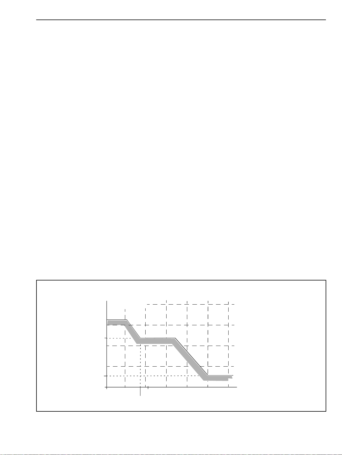
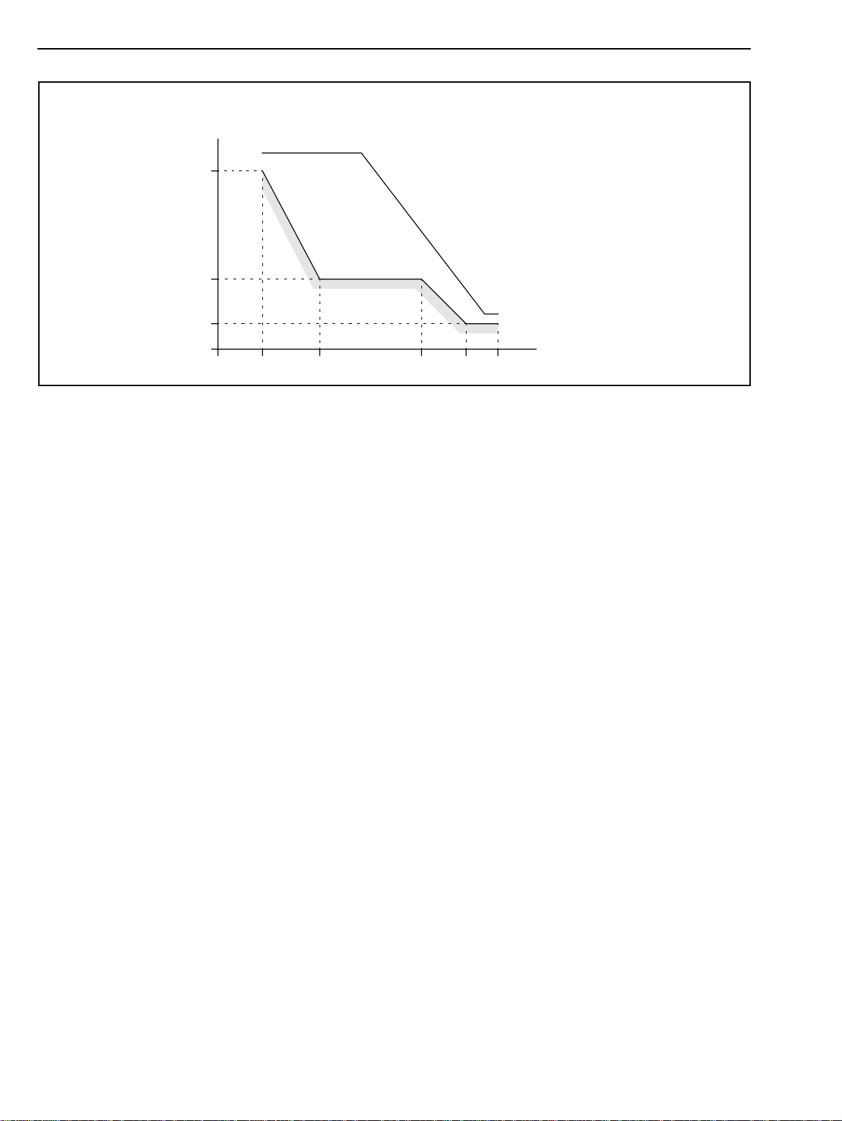
The jitter tolerance of the clock extractor circuit exceeds the requirements of TR 62411 in T1 mode (see Figure
3) and G.823 in E1 mode (see Figure 4).
Peak to Peak
Jitter Amplitude
(log scale)
138UI
100UI
28UI
10UI
1.0UI
0.4UI
1.0Hz 10Hz 1.0kHz 10kHz 100kHz
0.1Hz 100Hz
4.9Hz
Jitter Frequency
(log scale)
Figure 3 - Input Jitter Tolerance as Recommended by TR-62411 (T1)
17
MT9076 Preliminary Information
Peak to Peak
Jitter Amplitude
(log scale)
18UI
MT9076
Tolerance
1.5UI
0.2UI
1.667Hz 20Hz 2.4kHz 18kHz 100kHz
Jitter Frequency
(log scale)
Figure 4 - Input Jitter Tolerance as Recommended by G.823 and ETSI 300 011 (E1)
1.2 Transmitter
The transmit portion of the MT9076 LIU consists of a high speed digital-to-analog converter and
complementary line drivers.
When a pulse is to be transmitted, a sequence of digital values (dependent on transmit equalization) are read
out of a ROM by a high speed clock. These values drive the digital-to-analog converter to produce an analog
signal, which is passed to the complementary line drivers.
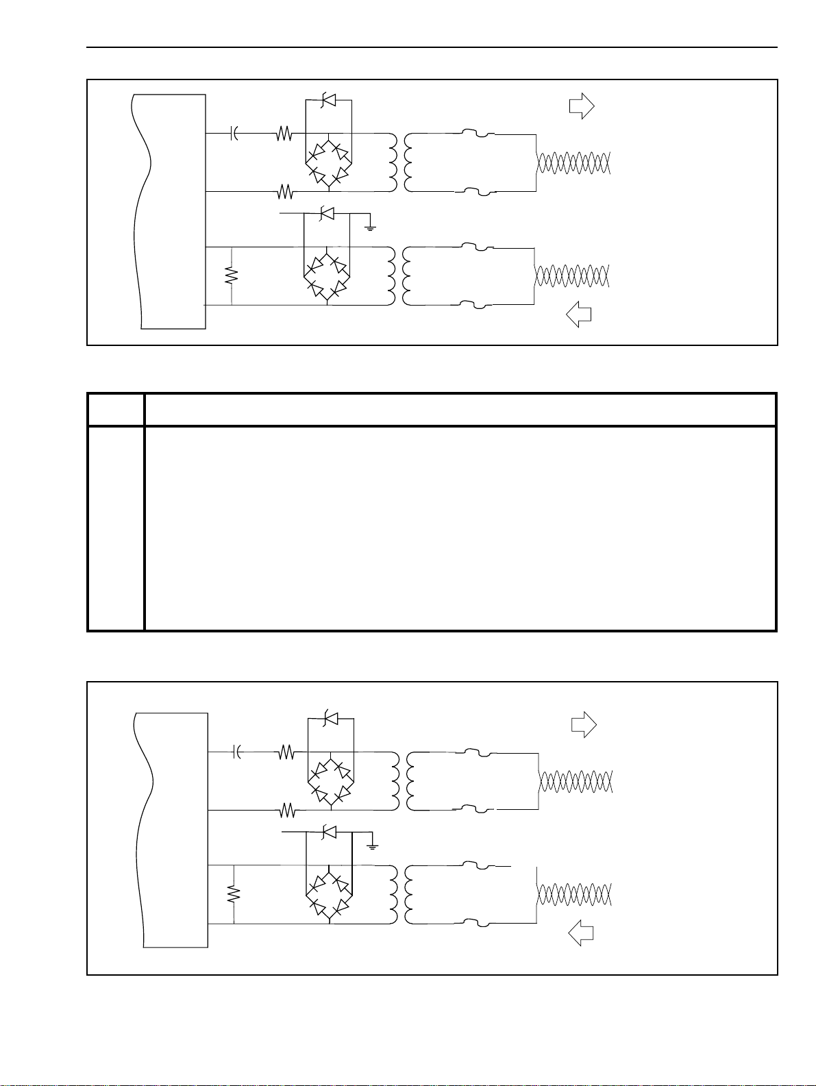
The complementary line drivers are designed to drive a 1:2.4 step-up transformer in T1 mode (see Figure 4 for
T1 mode) and either a 1:2 or 1:2.4 step-up transformer in E1 mode (see Figure 5 for E1 mode). A 0.47uF
capacitor is required between the TTIP and the transmit transformer. Resistors RT (as shown in Figure 4) are
for termination for transmit return loss. The values of RT may be optimized for T1 mode, E1 120Ω lines, E1 75Ω
lines or set at a compromise value to serve multiple applications. Program the Tx LIU Control Word (page 02H,
address 11H) to adjust the pulse amplitude accordingly.
Alternatively, the pulse level and shape may be discretely programmed by writing to the Custom Pulse Level
registers (page 2, addresses 1CH to 1FH) and setting the Custom Transmit Pulse bit high (bit 3 of the Tx LIU
Control Word). In this case the output of each of the registers directly drives the D/A converter going to the line
driver. Tables 1 and 2 show recommended transmit pulse amplitude settings.
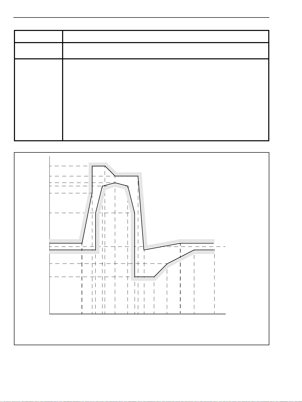
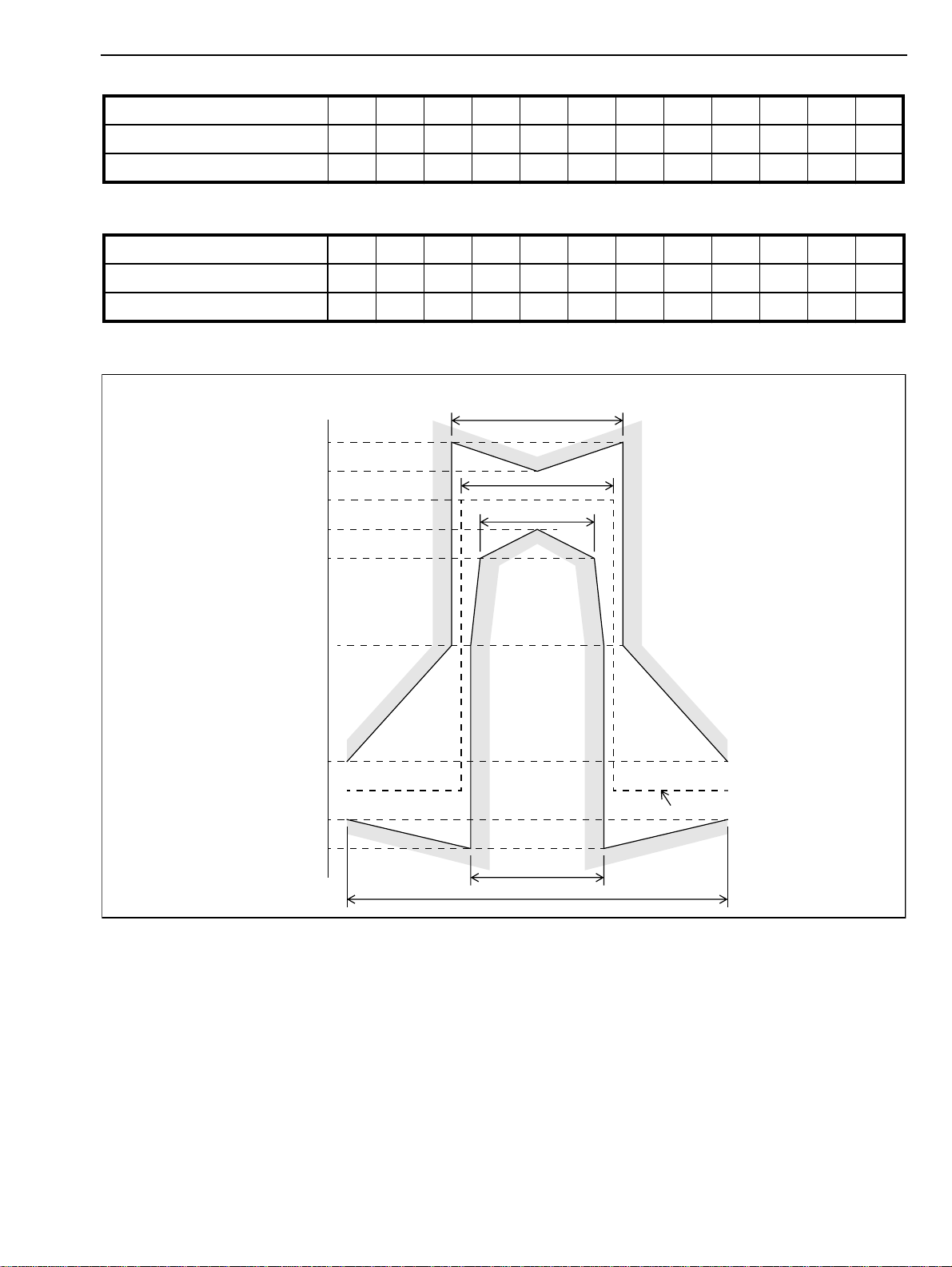
In T1 mode, the template for the transmitted pulse (the DSX-1 template) is shown in Figure 8. The nominal
peak voltage of a mark is 3 volts. The ratio of the amplitude of the transmit pulses generated by TTIP and
TRING lie between 0.95 and 1.05.
In E1 mode, the template for the transmitted pulse, as specified in G.703, is shown in Figure 8. The nominal
peak voltage of a mark is 3 volts for 120 Ω twisted pair applications and 2.37 volts for 75 Ω coax applications.
The ratio of the amplitude of the transmit pulses generated by TTIP and TRING lie between 0.95 and 1.05.
18
Preliminary Information MT9076
TTIP
TRING
RTIP
RRING
0.47uF
+3.3 V
17.36 Ω
R
T
R
T
1:2.4
1:2.4
Fuse
Tx
Fuse
RT: 2.4 Ω
Fuse
Fuse
Rx
Figure 5 - Analog Line Interface (T1)
Name Functional Description
TXL2-0 Transmit Line Build Out 2 - 0. Setting these bits shapes the transmit pulse as detailed in the table
below:
TXL2 TXL1 TXL0 Line Build Out
0 0 0 0 to 133 feet/ 0 dB
0 0 1 133 to 266 feet
0 1 0 266 to 399 feet
0 1 1 399 to 533 feet
1 0 0 533 to 655 feet
1 0 1 -7.5 dB
1 1 0 -15 dB
1 1 1 -22.5 dB
After reset these bits are zero.
TTIP
TRING
RTIP
RRING
0.47uF
20.83 Ω
RT
+3.3V
Table 1 - Transmit Line Build Out (T1)
1:2.4 (WR=0)
1:2 (WR=1)
RT
1:2.4
Fuse
Fuse
Fuse
Fuse
Figure 6 - Analog Line Interface (E1)
Tx
RT: Termination resistor. Please check
Table 2 for specific
resistor values.
Rx
19
MT9076 Preliminary Information
Name Functional Description
WR Winding Ratio. Set this pin low if a 1:2.4 transformer is used on the transmit side. Set this
pin high if a 1:2 transformer is used.
TX2-0 Transmit pulse amplitude. Select the TX2 –TX0 bits according to the line type, value of
termination resistors (RT), and transformer turns ratio used
TX2 TX1 TX0 Line Impedance(Ω) RT (Ω) Transformer Ratio
WR=0 WR=1 WR=0 WR=1
0 0 0 120 0 0 1:2.4 1:2
0 0 1 120 0 0 1:1 1:1
0 1 0 120 10.4 15 1:2.4 1:2
0 1 1 120 / 75 8.4 12.1 1:2.4 1:2
1 0 0 75 0 0 1:2.4 1:2
1 0 1 75 0 0 1:1 1:1
1 1 1 75 6.5 9.1 1:2.4 1:2
1 1 1 75 / 120 8.4 12.1 1:2.4 1:2
After reset these bits are zero.
Table 2 - Transmit Pulse Amplitude (E1)
1.20
1.05
0.95
0.90
0.80
0.50
0.05
0
-0.05
NORMALIZED AMPLITUDE
-0.26
-0.45
NOTE: 1 Unit Interval = 648 nanoseconds
20
-0.39
-0.27
-0.23
--0.12
--0.15
Time, in unit intervals (UI)
Figure 7 - Pulse Template (T1.403)(T1)
0
0.15
0.23
0.27
0.34
0.46
0.61
0.77
0.93
1.16
Preliminary Information MT9076
Time (Nanoseconds) -499 -253 -175 -175 -78 0 175 220 499 752 --- ---
Time U.I. -.77 -.39 -.27 -.27 -.12 0 .27 .34 .77 1.16 --- ---
Normalized Amplitude .05 .05 .8 1.2 1.2 1.05 1.05 -.05 .05 .05 --- ---
Table 3 - Maximum Curve for Figure 8
Time (Nanoseconds) -499 -149 -149 -97 0 97 149 149 298 395 603 752
Time U.I. -.77 -.23 -.23 -.15 0 .15 .23 .23 .46 .61 .93 1.16
Normalized Amplitude -.05 -.05 .5 .9 .95 .9 .5 -.45 -.45 -.26 -.05 -.05
Table 4 - Minimum Curve for Figure 8
Percentage of Nominal
Peak Voltage
120
269nS
110
100
90
80
50
20
-10
-20
244nS
194nS
0
Nominal Pulse
219nS
488nS
Figure 8 - Pulse Template (G.703)(E1)
1.3 20 Mhz Clock
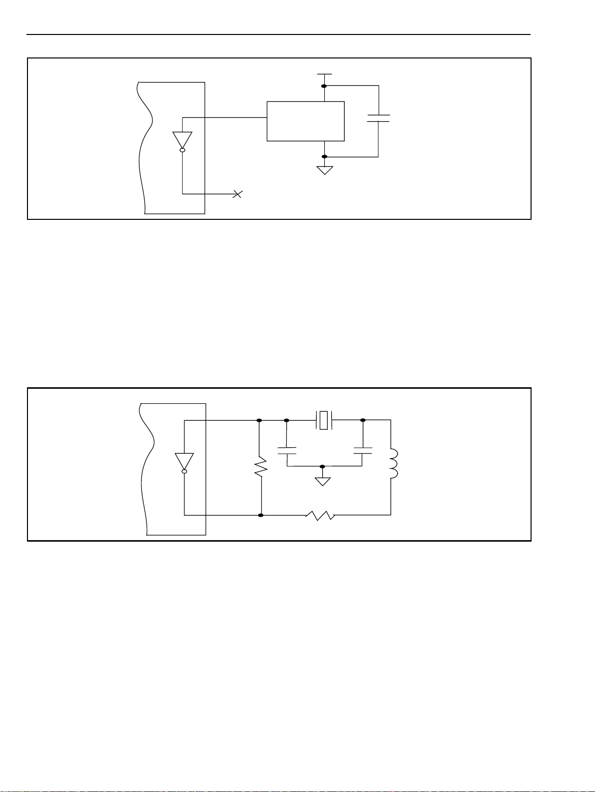
The MT9076 requires a 20 Mhz a clock. This may provided by a 50 ppm oscillator as per Figure 10.
21
MT9076 Preliminary Information
+3.3V
OSC1
OSC2
20MHz
OUT
(open)
Vdd
GND
.1µF
Figure 9 - Clock Oscillator Circuit
Alternatively, a crystal oscillator may be used. A complete oscillator circuit made up of a crystal, resistors and
capacitors is shown in Figure 10. The crystal specification is as follows.
Frequency: 20MHz
Tolerance: 50ppm
Oscillation Mode: Fundamental
Resonance Mode: Parallel
Load Capacitance: 32pF
Maximum Series Resistance: 35
Ω
Approximate Drive Level: 1mW
20MHz
OSC1
56pF
1MΩ
OSC2
39pF
1µH*
100Ω
Note: the 1µH inductor is optional
Figure 10 - Crystal Oscillator Circuit
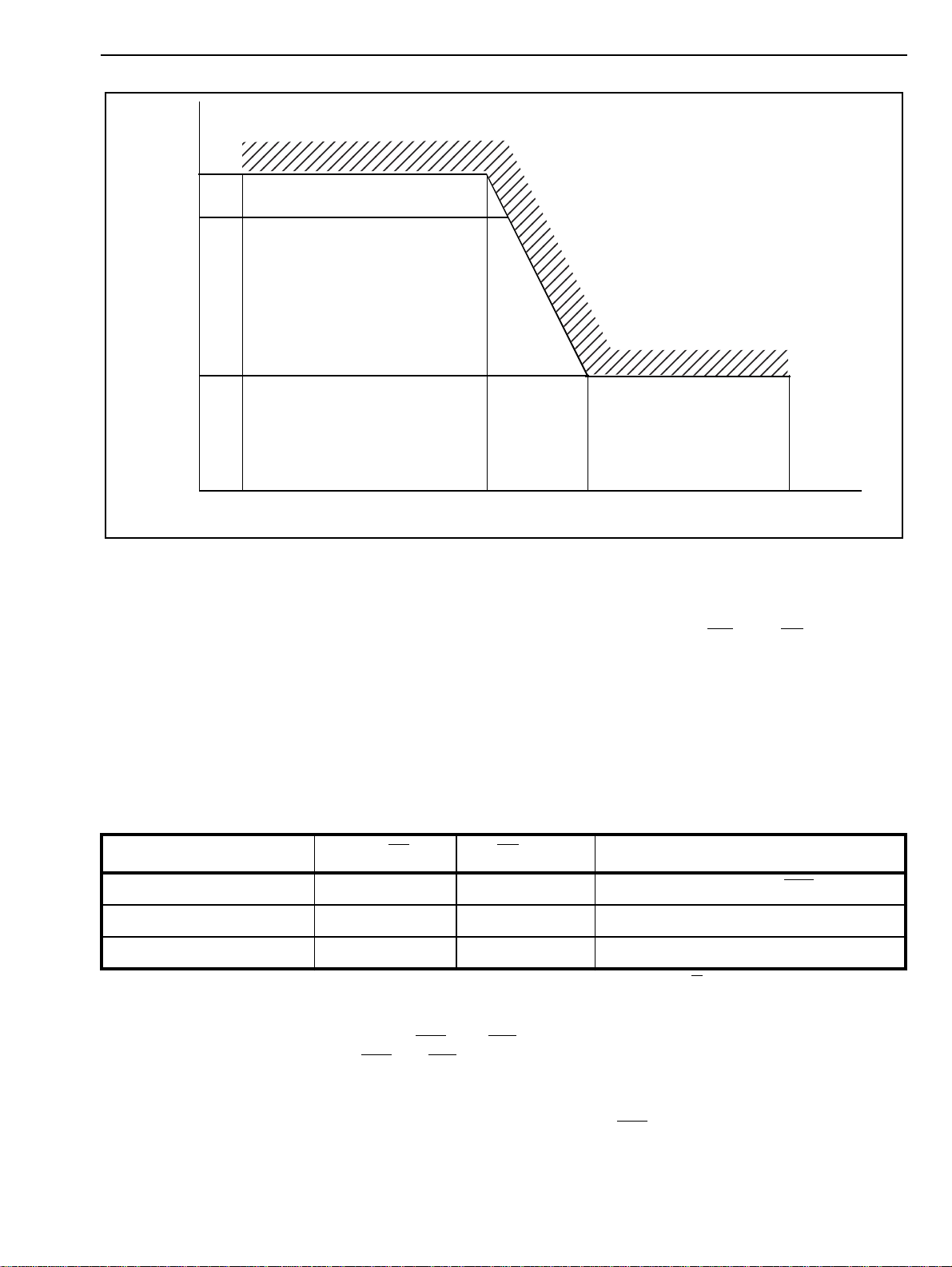
1.4 Phase Lock Loop (PLL)
The MT9076 contains a PLL, which can be locked to either an input 4.096 Mhz clock or the extracted line
clock.The PLL will attenuate jitter from less than 2.5 Hz and roll-off at a rate of 20 dB/decade. Its intrinsic jitter
is less than 0.02 UI. The PLL will meet the jitter transfer characteristics as specified by AT&T document
TR 62411and the relevant recommendations as shown in Figure 12.
22
Preliminary Information MT9076
dB
-0.5
0
-20 dB/decade
JITTER ATTENUATION (dB)
19.5
10 40 400 10K
Frequency (Hz)
Figure 11 - TR 62411 Jitter Attenuation Curve
2.0 Clock Jitter Attenuation Modes
MT9076 has three basic jitter attenuation modes of operation, selected by the BS/LS and S/FR/Exclki control
pins.
• System Bus Synchronous Mode
• Line Synchronous Mode
• Free-run mode
Depending on the mode selection above, the PLL can either attenuate transmit clock jitter or the receive clock
jitter. Table 5 shows the appropriate configuration of each control pin to achieve the appropriate mode and
Jitter attenuation capability of the MT9076.
Mode Name BS/LS S/FR/Exclki Note
System Bus Synchronous 1 1 PLL locked to C4b.
Line Synchronous 0 1 PLL locked to Exclk.
Free-Run x 0 PLL free - running.
Table 5 - Selection of clock jitter attenuation modes using the M/S and MS/FR pins
In System Bus Synchronous mode, pins C4b and F0b are always configured as inputs, while in the Line
Synchronous and Free-Run modes C4b and F0b are configured as outputs.
Referring to the mode names given in Table 5 the basic operation of the jitter attenuation modes are:
•In
System Bus Synchronous
mode an external clock is applied to C4b. The applied clock is dejittered by
the internal PLL before being used to synchronize the transmitted data. The clock extracted (with no
jitter attenuation performed) from the receive data can be monitored on pin Exclk.
23

MT9076 Preliminary Information
•In
Line Synchronous
and then output on pin C4b. Pin Exclk provides the extracted receive clock before it has been dejittered.
The transmit data is synchronous to the clean receive clock.
•In
Free-Run
is output on pin C4b. The clock signal extracted from the receive data is not dejittered and is output
directly on Exclk.
2.1 Jitter Attenuator FIFO
In System Bus Synchronous operation, a data buffer is required between the jittered input clock and the clean
transmit clock. In normal T1 mode, the transmit slip buffer performs this function. In T1 IMA mode, the transmit
slip buffer is unused, instead a jitter attenuator FIFO is employed. In an E1 mode System Bus Synchronous
configuration, the jitter attenuator FIFO is always used. In this case the C4b signal clocks the data into the
FIFO, the PLL de-jitters the C4b clock and the resulting clean C4b signal clocks the data out of the FIFO.
The JA meets the jitter transfer characteristics as proposed by ETSI ETS 300 011, G.735 and the relevant
recommendations as shown in Figure 12. The JA FIFO depth can be selected to be from 16 to 128 words deep ,
in multiples of 16 (2-bit) words. Its read pointer can be centered by changing the JFC bit (address 13H of page
02H) to provide maximum jitter tolerance. If the read pointer should come within 4 bits of either end of the
FIFO, the read clock frequency will be increased or decreased by 0.0625 UI to correct the situation. The
maximum time needed to centre is T
this time the JA will not attenuate jitter.
mode the transmit data is synchronized to the internally generated clock. The internal clock
mode, the clock extracted from the receive data is dejittered using the internal PLL
= 3904∗Depth ns, where Depth is the selected JA FIFO depth. During
max
2.2 IMA Mode
2.2.1 T1 Mode
In T1 IMA Mode, neither the transmit nor the receive slip buffers are activated. Channel Associated signaling
(CAS) and HDLC operation is not supported. The input pin C4b accepts a 1.544 MHz clock and it clocks
incoming data from DSTi into a jitter attenuator FIFO. This clock is dejittered with the internal PLL. The
dejittered clock clocks data out of the FIFO for transmission onto the line. Receive clock (1.544 MHz) and data
is extracted from the line and routed to pins Exclk and DSTo respectively. The receive clock Exclk is not
dejittered before being driven off chip. For operation in IMA mode, the MT9076 should be programmed in
System Bus Synchronous mode (BS/LS and S/FR/Exclki set high).
2.2.2 E1 Mode
In E1 IMA Mode neither the transmit nor the receive slip buffers are activated. The input pin C4b accepts a
2.048 MHz clock and it clocks incoming data from DSTi into a jitter attenuator FIFO. This clock is dejittered with
the internal PLL. The dejittered clock clocks data out of the FIFO for transmission onto the line. Receive clock
(2.048 MHz) and data is extracted from the line and routed to pins Exclk and DSTo respectively. The receive
clock Exclk is not dejittered before being driven off chip. For operation in IMA mode, the MT9076 should be
programmed in System Bus Synchronous mode (BS/LS and S/FR/Exclki set high).
3.0 The Digital Interface
3.1 T1 Digital Interface
In T1 mode, DS1 frames are 193 bits long and are transmitted at a frame repetition rate of 8000 Hz, which
results in an aggregate bit rate of 193 bits x 8000/sec= 1.544 Mbits/sec. The actual bit rate is 1.544 Mbits/sec
+/-50 ppm optionally encoded in B8ZS format. The Zero Suppression control register (page 1, address 15H,)
selects either B8ZS encoding, forced one stuffing or alternate mark inversion (AMI) encoding. Basic frames are
divided into 24 time slots numbered 1 to 24. Each time slot is 8 bits in length and is transmitted most significant
bit first (numbered bit 1). This results in a single time slot data rate of 8 bits x 8000/sec. = 64 kbits/sec.
24
Preliminary Information MT9076
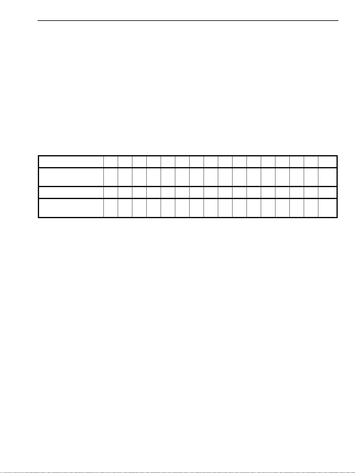
It should be noted that the Mitel ST-BUS has 32 channels numbered 0 to 31. When mapping to the DS1
payload only the first 24 time slots and the last (time slot 31, for the overhead bit) of an ST-BUS are used (see
Table 6). All unused channels are tristate.
When signaling information is written to the MT9076 in T1 mode using ST-BUS control links (as opposed to
direct writes by the microport to the on - board signaling registers), the CSTi channels corresponding to the
selected DSTi channels streams are used to transmit the signaling bits.
Since the maximum number of signaling bits associated with any channel is 4 (in the case of ABCD), only half
a CSTi channel is required for sourcing the signaling bits. The choice of which half of the channel to use is
selected by the control bit MSN (page 01H address 14H). The same control bit selects which half of the CSTo
channel will contain receive signaling information (the other nibble in the channel being tristate). Unused
channels are tristate.
The most significant bit of an eight bit ST-BUS channel is numbered bit 7 (see Mitel Application Note MSAN-
126). Therefore, ST-BUS bit 7 is synonymous with DS1 bit 1; bit 6 with bit 2: and so on.
DS1 Timeslots 12345678910111213141516
Voice/Data Channels
(DSTi/o and CSTi/o)
Ds1 Timeslots 17 18 19 20 21 22 23 24 ------- Voice/Data Channels
(DSTi/o and CSTi/o)
3.2 Frame and Superframe Structure in T1 mode
3.2.1 Multiframing
In T1 mode, DS1 trunks contain 24 bytes of serial voice/data channels bundled with an o verhead bit. The frame
overhead bit contains a fixed repeating pattern used to enable DS1 receivers to deliniate frame boundaries.
Overhead bits are inserted once per frame at the beginning of the transmit frame boundary. The DS1 frames
are further grouped in bundles of frames, generally 12 (for D4 applications) or 24 frames (for ESF - extended
superframe applications) deep. Table 7 and 8 illustrate the D4 and ESF frame structures respectively.
For D4 links the frame structure contains an alternating 101010... pattern inser ted into every second overhead
bit position. These bits are intended for determination of frame boundaries, and they are referred to as Ft bits.
A separate fixed pattern, repeating every superframe, is interleaved with the Ft bits. This fixed pattern
(001110), is used to deliniate the 12 frame superframe. These bits are referred to as the Fs bits. In D4 frames
# 6 and #12, the LSB of each channel byte may be replaced with A bit (frame #6) and B bit (frame #12)
signaling information.
0123456779101112131415
16 17 18 19 20 21 22 23 24x25x26x27x28x29x30x31
Sbit
Table 6 - ST-BUS vs. DS1 to Channel Relationship(T1)
For ESF links the 6 bit framing pattern 001011, inserted into every 4th overhead bit position, is used to
deliniate both frame and superframe boundaries. Frames #6, 12, 18 and 24 contain the A, B, C and D signaling
bits, respectively. A 4 kHz data link is embedded in the overhead bit position, interleaved between the framing
pattern sequence (FPS) and the transmit CRC-6 remainder (from the calculation done on the previous
superframe), see Table 8.
The SLC-96 frame structure is similar to the D4 frame structure, except a facility management overlay is
superimposed over the erstwhile Fs bits, see Table 9.
The protocol appropriate for the application is selected via the Framing Mode Selection Word, address 10H of
Master Control page 1. In T1 mode, MT9076 is capable of generating the overhead bit framing pattern and (for
ESF links) the CRC remainder for transmission onto the DS1 trunk. The beginning of the transmit multiframe
may be determined by any of the following criteria:
25

MT9076 Preliminary Information
(i) It may free - run with the internal multiframe counters;
(ii) The multiframe counters may be reset with the external hardware pin TxMF. If this signal is not
synchronous with the current transmit frame count it may cause the far end to go temporarily out of sync.
(iii) Under software control (by setting the TxSYNC bit in page 01 address 12H) the transmit multiframe
counters will be synchronized to the framing pattern present in the overhead bits multiplexed into channel
31 bit 0 of the incoming 2.048 Mb/s digital stream DSTi. Note that the overhead bits extracted from the
receive signal are multiplexed into outgoing DSTo channel 31 bit 0.
(iv) In SLC - 96 mode the transmit frame counters synchronize to the framing pattern clocked in on the TXDL
input
Frame # Ft Fs Signaling
11
20
30
40
51
61A
70
81
91
10 1
11 0
12 0 B
Table 7 - D4 Superframe Structure(T1)
Frame # FPS FDL CRC Signaling
1X
2 CB1
3X
40
5X
6 CB2 A
7X
80
9X
10 CB3
11 X
12 1 B
13 X
14 CB4
15 X
16 0
17 X
18 CB5 C
19 X
20 1
21 X
22 CB6
23 X
24 1 D
Table 8 - ESF Superframe Structure (T1)
26
 Loading...