MITEL MT90733AP Datasheet

CMOS
DS3 Framer (DS3F)
MT90733
Advance Information
Features
• DS3 payload access in either bit-serial or
nibble-para ll el m o de
• C-bit parity or M 13 op erating mode
• Separate interface f or C-bi ts
• Detect and genera te DS 3 AIS, and id le sign als
• Transmit referenc e ge nerat or for se rial
operation
• Transmit and rec eive FEAC chan ne l under
software control
• Transmit single errors: framing, FEBE, C-bit
parity, and P-bit parity
• FEBE, C-bit and P-bit performance counters
• Transmit-to-Receive and Receive-to-Transmit
loopbacks
Applications
• Sub rat e mul t iple x ing
• Wideban d dat a or vide o tran spor t
• DS3 moni tor an d test
• Channel extenders
ISSUE 1 May 1995
Ordering Information
MT90733AP 68 Pin PLCC
-40° to 85°C
Description
The MT90733 DS3 Framer (DS3F) is designed for
mapping broadband payloads into the DS3 frame format, which meets ANSI’s T1.107-1988 and supplement T1.107a-1990.
Although the C -bit parity format is re commended, the
DS3F can also operat e in the M13 m ode. In the C-bit
parity format, the DS3F provides a separate interfa ce
for selected C-bits. The DS 3F also provides software
access for transmitting and receiving the FEAC channel, and generates and dete cts DS3 AI S, DS3 idle, Pbit parity and C-bit parity. In addition, performance
counters are provided, as well as the ability to generate single framin g, FEBE, C-bit pa rity and P-bit parity
errors. The payload interface is selectable through
software as either a bit-serial or nibble-parallel format.
X1
X2
FE
D3RD
D3RC
CRD
CRCK
CRF
CRDCC
STUFC
STUFD
AD(7-0)
WR
RD
ALE
SEL
OENA
FORCEOE
CXD
CXCK
CXF
CXDCC
D3TD
D3TC
FORCECP
FORCEPP
FORCFEBE
Line Side
DS3
Receive
µP I/O
DS3
Send
DS3
Interpreter
Receive
Transmit
Terminal Side
Output
Transm it
Frame
Reference
Generato r
Input
Parallel
Serial
N.C.
RNIB3
N.C.
RNIB2
N.C.
RNIB1
RDS
RNIB0
RCS
RCN
RCG
N.C.
RFN
RFS
TDOUT
TCG
TFOUT
TCOUT
TFIN
TCIN
XFNO
N.C.
N.C.
XCN
XCK
XCK
XFSI
N.C.
XNIB3
XDS
XNIB2
N.C.
XNIB1
N.C.
N.C. XNIB0
U.S. Patent Number 504017 0
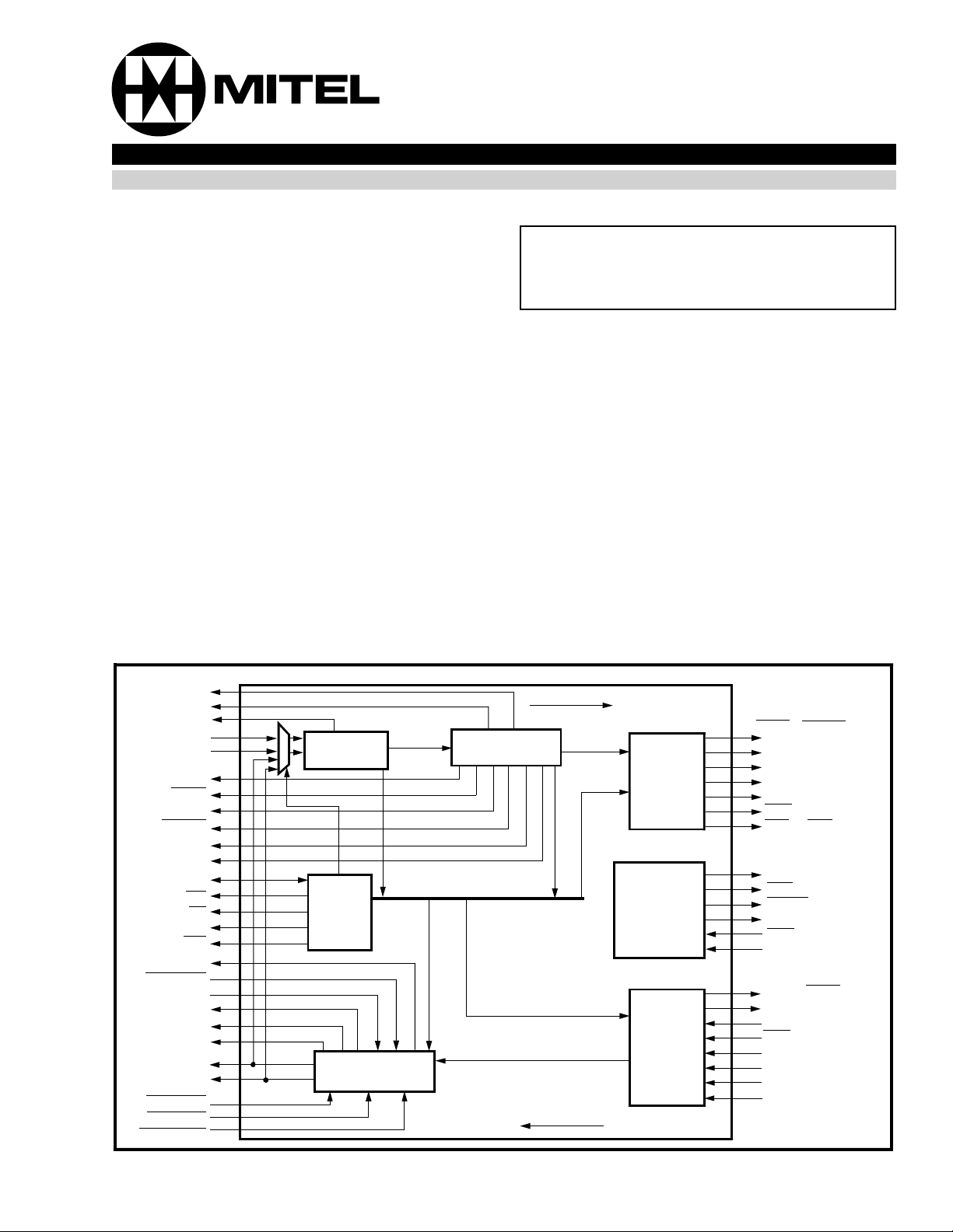
Figure 1 - Functional Block Diagram
5-23

MT90733 CMOS Advance Information
ALE
X1
RD
X2
WR
STUFD
STUFC
VDD
AD7
AD6
AD5
AD4
VSS
AD3
AD2
AD1
AD0
OENA
SEL
TEST
VSS
D3RC
VDD
D3TD
XFNO
D3TC
CXCK
VSS
XNC
CXF
CXDCC
10
9
8
7
6
5
4
3
2
1
6867666564
11
12
13
14
15
16
17
18
19
20
21
22
23
24
25
26
282930313233343536373839404142
27
VSS
RCS/RCN
CRF
CRCK
VDD
CRD
RNIB3
RNIB2
VDD
CXD
D3RD
CRDCC
RCG
RFS/RFN
FORCfEBE
VDD
XCK
61
XNIB0
60
63
62
59
XNIB1
58
XNIB2
57
FORCECP
XDS/XNIB3
56
FORCEPP
55
FORCEOE
54
VSS
53
TCIN
52
VDD
51
XFSI
50
TFIN
49
TCOUT
48
TFOUT
47
TCG
46
TDOUT
45
VSS
43
44
FE
RNIB1
RDS/RNIB0
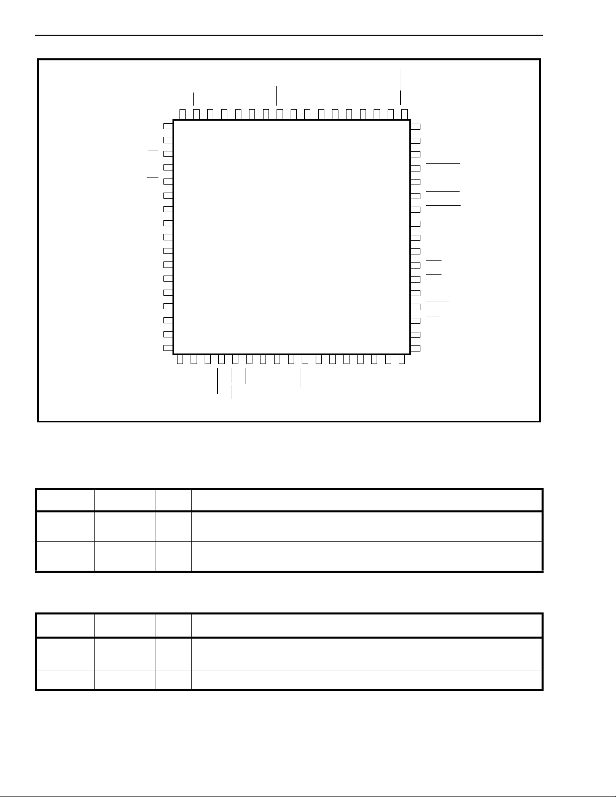
Figure 2 - Pin Connections
Pin Description
Power Supply & Ground
Pin # Name I/O/P Description
4, 17, 27
38, 51, 63
6, 22, 33
44, 53, 67
Note: I = In pu t; O = O u tp ut; P = Po w er
DS3 Receive Line Side Interface
Pin # Name I/O/P Description
5 D3RC I DS3 Receive Cloc k. A 44.736 MHz clock used for clocking in receive data,
29 D3RD I DS3 Receive Data. DS3 line side serial receive data.
Note: I = In pu t; O = O u tp ut; P = Po w er
VDD P Power Supp l y Input. +5v± 5%.
VSS P Ground.
and as the time base for the DS3F receiver.
5-24

Advance Information CMOS MT90733
DS3 Transmit Line Side Interface
Pin # Name I/O/P Description
1 D3TC O DS3 Transmit Clock. A 44.736 MHz clock that is derived from the transmit
clock (XCK) signal and is used for clocking out the line side DS3 data signal.
3 D3T D O DS 3 Transmit Data. DS3 line side serial transmit data.
Note: I = In pu t; O = O u tp ut; P = Po w er
Receive Terminal Side Interfac
e
Pin # Name I/O/P Description
31
RFS/RFN O Receive Fram ing Pulse for S eri al/Ni bble In terface. The fram ing pulse is
synchronous with the first bit 1 in the DS3 frame or nibble 1175.
32 RCG
O Receive Clock Gap Signal. The active low gap signal is synchro nous with
each overhead bit in the serial DS3 frame (first bit in the 85-bit group).
34 RCS/RCN O Receive Clock for Serial/Nibble Interface. Clock used for clocking out the
terminal side receive serial and nibble data .
39
40
41
42
Note: I = In pu t; O = O u tp ut; P = Po w er
Transmit Terminal Side Inter fac
RNIB3
RNIB2
RNIB1
RDS/RNIB0
O Receive Nibble/Serial Interface. Nibble data is clocked out on positive transi-
tions of the nibble clock (RCN). Serial data is clocked out on negative transitions of the receive clock (RCS).
e
Pin # Name I/O/P Description
2
XFNO
O Transmit Framing Pulse for Nibble Interface. An active low , one nibble clock
cycle wide (XCN) pulse that occurs during the second nibble time.
50
XFSI
I Transmit Framing Pulse for Serial Interface: A framing pulse input that must
be synchronous with bit 1 in the transmit serial data DS3 frame.
56
58
59
60
XDS/XNIB3
XNIB2
XNIB1
XNIB0
I Transmit Nibble/Serial Interface. Nibble data is clocked in on positive transi-
tions of the nibble clock (XCN). Serial data is clocked into the DS3F on positive transitions of the transmit clock (XCK).
62 XCK I Transmit Clock. A 44.736 Mbit/s cl oc k input with a stabili ty of ±20 ppm and a
duty cycle of 50 ±10%. XCK provides the tim e base for the transm itte r in the
DS3F.
66 XCN O Transmit Clock for Nibble Interface . Output clock signal derived from the
transmit clock (XCK).
Note: I = In pu t; O = O u tp ut; P = Po w er
5-25
 Loading...