MITEL MT90732AP Datasheet

CMOS
MT90732
E2/E3 Framer (E2/E3F)
Advance Information
Features
• Framer for CCITT Recommendations
- G.742 (8448 kbit/s)
- G.745 (8448 kbit/s)
- G.751 (34368 kbit/s)
- G.753 (34368 kbit/s)
• Line side interfac e
- Dual rail or NRZ
• HDB3 code c for dual rail I/O
• Terminal side interface
- Nibble-parallel
- Bit-serial
• Transmit reference generator for bit-serial I/O
• Microprocesso r or control leads
• I/O port for servic e bits
Applications
• Line term inals
• Wideban d dat a or vide o tran spor t
• Test e quipm ent
• Multiplexer systems
ISSUE 1 May 1995
Ordering Information
MT90732AP 68 Pin PLCC
-40°C to +85°C
Description
The MT90732 E2/E3 Framer (E2/E3F) is a CMOS
VLSI device that provides the functions needed to
frame a wideband payload to one of four CCITT
Recommendations. G. 742, G.745, G.751, or G.753.
The E2/E3 Framer interfaces to line circuitry with
either dual rail or NRZ signals. On the terminal side,
the interface can be either nibble-parallel or bitserial.
The MT90732 can be operated with or without a
microprocessor. When interfaced with a
microprocessor, the E2/E3 Framer provides an 8byte memory map for control, performance counters
and alarm st atus. The MT90732 provides a transmit
and receive interface port for accessing the
overhead bits from each of the four
recommendations. The overhead bits can also be
accessed by the microprocessor via the memory
map.
RDL
RCKL
RP/RDL
RN
RCK/RCKL
CV
RAIS
RLOC
BIP-4E
RLOF
ROD
ROC
ROF
FE
NRZ LINE
BIP-4
M0
M1
MICRO
SER
DAIS
TLBK
PLBK
TAIS
LPT
TLCINV
TLOC
FORCEFE
TOD
TOC
TOF
RESET
TP/TDL
TCK/TCKL
Line Side Terminal Side
U.S. Patent Number 5040170
TN
TCKL
TDL
Line
Decoder
Control
Line
Encoder
Data
Clock
Data
Clock
Framer
G.7XX
Send
Data
Clock
Frame
Clock
Data
Framing
Interpreter
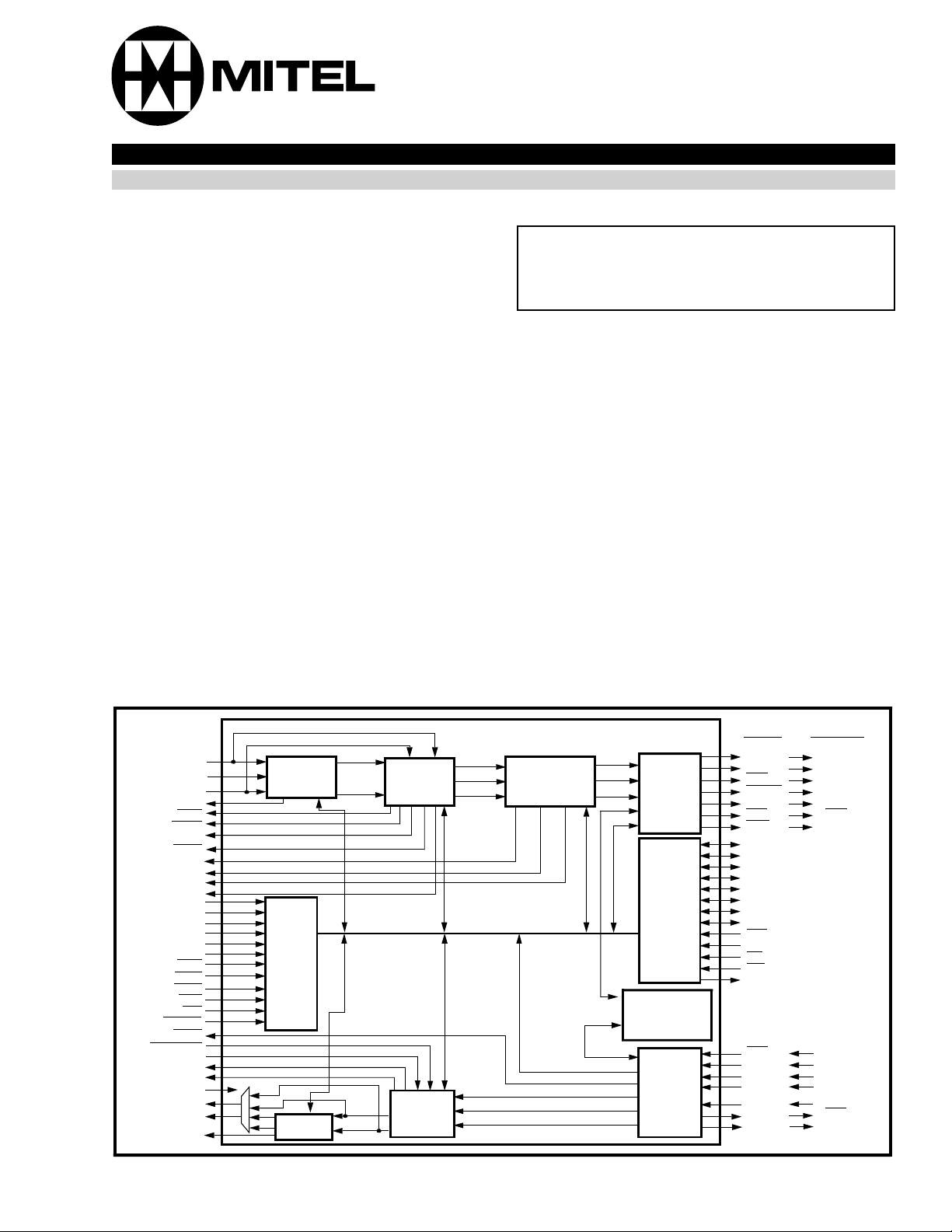
Figure 1 - Functiona l Block Diagram
Data
Clock
Frame
Output
Micro-
processor
I/O
Transmit
Reference
Generator
Input
SERIAL
RSD
TDOUT
TCG
TFOUT
RSC
RSF
RCG N.C.
AD7
AD6
AD5
AD4
AD3
AD2
AD1
AD0
SEL
ALE
RD
WR
RDY
XSF
N.C.
TCIN
XSD
XCK
N.C.
TCOUT
P ARALLEL
RNIB3
RNIB2
RNIB1
RNIB0
RNC
RNF
XNIB3
XNIB2
XNIB1
XNIB0
XCK
XNF
XNC
5-15

MT90732 CMOS Advance Information
/RSF
RCG
RNIB3/RSD
RNF
61
BIP-4E
60
59
XNC/TCOUT
58
XNF
57
XCK
56
XNIB0/XSD
55
XNIB1/TCIN
54
XNIB2
53
XNIB3/XSF
GND
52
VDD
51
TLCINV
50
DAIS
49
RDY
48
WR
47
RD
46
ALE
45
SEL
43
44
AD0
AD2
AD1
ROC
ROF
FE
NRZLINE
BIP-4
M0
M1
VDD
GND
MICRO
SER
TLBK
PLBK
TAIS
LPT
TLOC
FORCEFE
ROD
RLOF
RLOC
RAIS
CV
RCK/RCKL
RN
RP/RDL
VDD
GND
RNC/RSC
RNIB0/TFOUT
RNIB1/TCG
RNIB2/TDOUT
10
9
8
7
6
5
4
3
2
1
68676665646362
11
12
13
14
15
16
17
18
19
20
21
22
23
24
25
26
282930313233343536373839404142
27
TOF
TOD
TOC
RESET
TN
TP/TDL
TCK/TCKL
AD7
AD6
AD5
AD4
VDD
GND
AD3
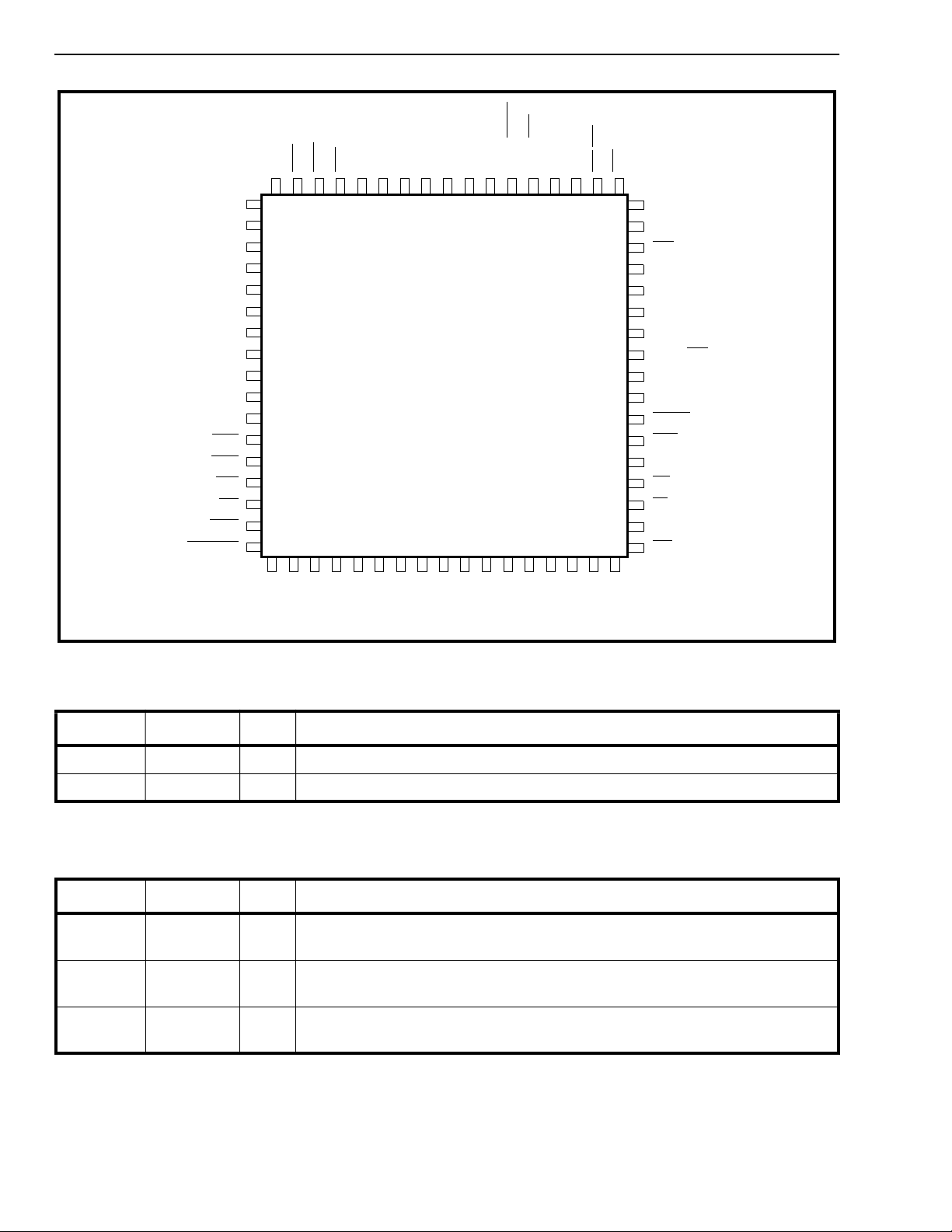
Figure 2 - Pin Connections
Pin Description
Power Supply and Ground
Pin # Name I/O/P Description
1,17,35,51 VDD P VDD. 5-volt supply voltage, +/- 5%
18,34,52,6 8 GND P Ground .
Note: I = Input; O = Output; P = Power
Line Side Receiv e
Pin # Name I/O/P Description
2 RP/RDL I Receive Pos itive Rail /Recei ve NRZ Data. Recei ve positive rail/NRZ dat a
generated from line interface circuit.
3RNIReceive Negative Rail Data. Receive negative rail dat a generat ed from line
interface circuit.
4 RCK/RCKL I Receive Clock Rail/Receive Clock NRZ. The receive clock is used for clock-
ing in the rail/NRZ data signals.
Note: I = Input; O = Output; P = Power
5-16

Advance Information CMOS MT90732
Line Side Transmit
Pin # Name I/O/P Description
31 TP/TDL O Transmit Positive Rail/Transmit NRZ Data. Transmit positive rail/NRZ data
sent out of E2/E 3 F ram e r.
32 TCK/TCKL O Transmit Clock Rail/Transmit Clock NR Z. The transm it clo ck is used for
clocking out the dual rail/NRZ data signals. The TCK/TCKL clock signal is
derived from the XCK clock.
33 TN O Transmit Negative Rail Data. Transmit negative rail data sent out of E2/E3
Framer.
Note: I = Input; O = Output; P = Power
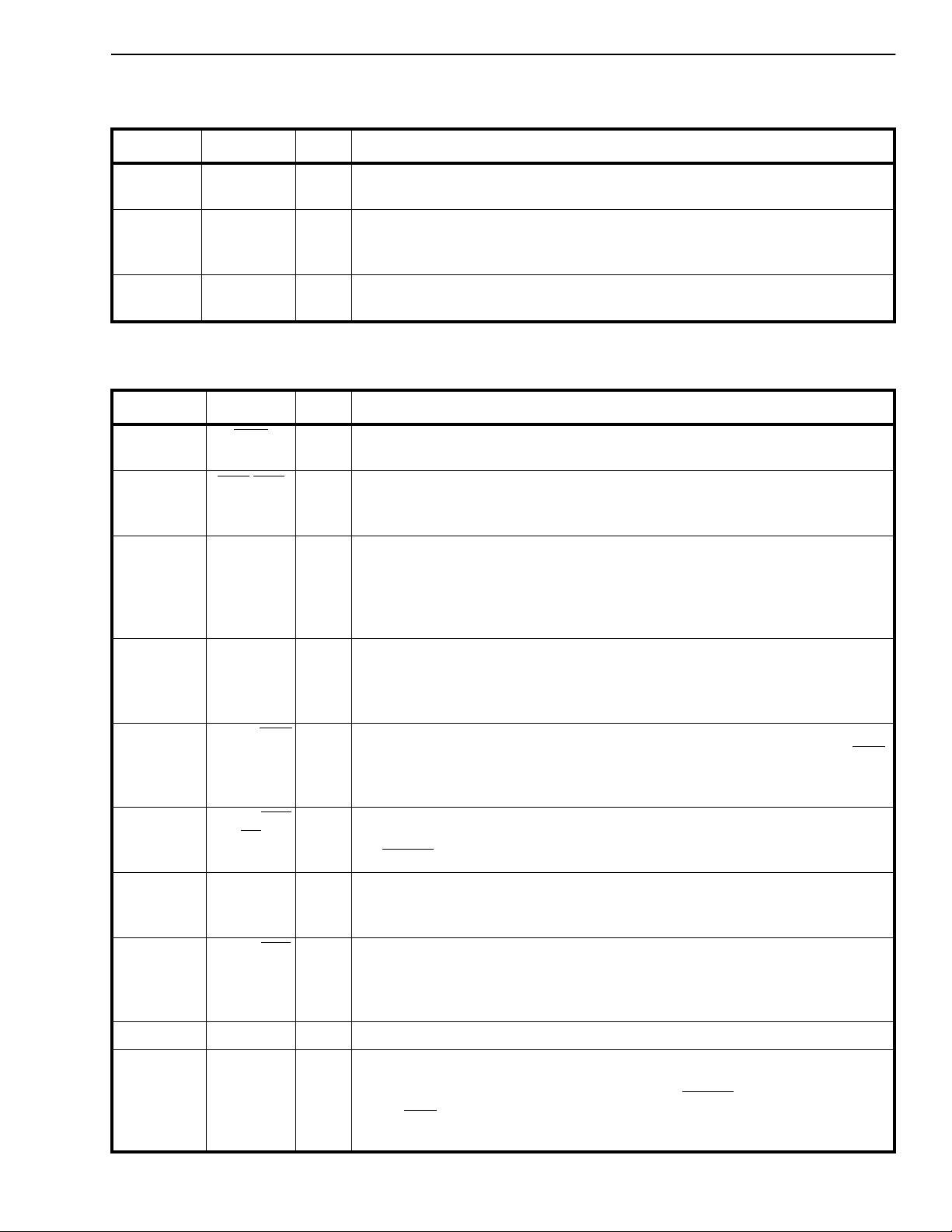
T erminal Interface
Pin # Name I/ O/P Description
61 RCG
62 RNF
63 RNIB3/RSD O Receive Nibble Bit 3/Receive Serial Data. Bit 3 is the most significa nt bit in
64 RNIB2/TDOUTO Receive Nibble Bit 2/Transmit Reference Generator Data Outpu t. In t h e
65 RNIB1/TCG
66 RNIB0/T FO
67 RNC/RSC O Receive Nibble Clock/Receive Serial Clock. The nibble and serial clocks are
/RSF O Receive Framing Pulse. Framing pulse is synchronous with the last nibble for
UT
O Receive Clock Gapped. An active low signal indi cates the receive framin g
and service bit locations in the serial mode only.
the nibble-parallel inte rface, and with the first bit in the frame for the bit-serial
interfac e.
the nibble and corresponds to the first bit received in the nibble. The framing
pattern, service bits, and BIP-4 nibble are not provided as parallel dat a. In the
serial mode receive data signal consists of all bits, including the framing pattern and service bits.
nibble-parallel m ode, it is Bit 2 of the received nibble.The reference generat or
is enabled in the serial mode. The output data signal (TDOUT) consists of all
ones in place of the frami ng bits and zeros elsewhere in the f ra me.
O Receive Nibble Bit 1/Transmit Reference Generator Clock Gap Signal. In
the nibble-parallel mod e, it is Bit 1 of the received nibble. The active low TCG
signal indicates the location of the framing pattern and the service b its in the
frame.
O Receive Nibble Bit 0/Transmit Reference Generator Framing Pulse. Bit 0
is the least significant bit in the nibble and is the last bit receive d. The active
low TFOUT
derived from the line side dual rail/N RZ clo ck signal (RCK/RCK L). RNC is
gapped during framing patt ern, service bit and BIP-4 bit times.
signal is synchronous with the first bit in the frame.
53 XNIB3/XSF
54 XNIB2 I Transmit Nibb le Bi t 2. Bit 2 in the 4-bit nibble.
55 XNIB1/TCI
N
I Transmit Nibble Bit 3/Transmit Serial Framing Pu lse. In the nibble-parallel
mode, bit 3 is the most significant bit in the nibble and corresponds to the first
bit transmitted in the nibble. When the terminal interface is serial, the negative
framing pulse is synchronous with the first bit in the frame.
I Transmit Nibble Bit 1/Transmit Reference Generator Clock I n. Bit 1 in the
transmit nibble. For a serial interface, the TCIN is used to derive the clock out
(TCOUT), data signal (TDOUT), framin g pulse (TFO UT
signal (TCG
external payload data into the serial frame.
).The reference generator signals are provided for multiplexing the
), and gapped clock
5-17
 Loading...