MITEL MT90710AP Datasheet

CMOS
MT90710
High-Speed Isochronous Multiplexer
Preliminary Information
Features
• Multiplexe s eight 2.048 M bit/ s, ST-BUS links
onto one seri al hig h-spee d 20 .48 Mbi t/s link
• 15.808 Mbit/s clear bandwidth transport
• Two 8 kbit/s and one 32 k bit/s o versa mpled
signalling cha nnels
• Embedded system timing and frame
synchronization
• Frame buffer co ntrol s ignals gener ated on-ch ip
• Check-su m gen erate d on multipl exe d fram e
• Remote synchronization indication
• Both mas ter an d slave t iming mode ope ration
• On-chip re ferenc e gene ration f or slave mode
synchronization
• 4B/5B data encoding/decoding
Applications
• Fibre distributed sytems
• Backpla ne conc ent rato rs
• Local Area Networks (LANs)
ISSUE 1 January 1995
Ordering Information
MT90710AP 84 Pin PLCC
0 °C to +70 °C
Description
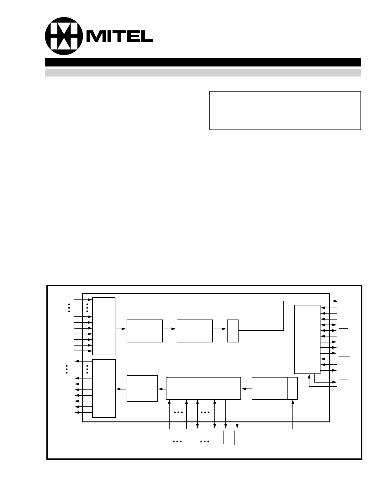
The High-Speed Isochronous Multiplexer integrated
circuit multiplexes up to eight Serial Telecom
(ST-BUS) links onto a single 20 MHz loop to facilitate
point-to-point data transport requirements. The
MT90710 connects easily with standard Fiber Optic
interfaces to form a complete electric to photonic
conversion circuit. Optical transmission allows large
bandwidth inter-shelf or, in distributed systems,
inter-node communication by eliminating multiple
data buses, cable inter-connect and attendant driver
interfaces. The final result is a simple physical
interface free of the radiated emissions and
background noise susceptibility problems
encountered in copper-wired environments.
STi0
STi5
STi6A
STi6B
STi7
DIN8K0
DIN8K1
DIN32K
STo0
STo5
STo6A
STo6B
STo7
DOUT8K0
DOUT8K1
DOUT32K
MUX
DEMUX
TRANSMIT
Overhead
Checksum
Frame Sync
RECEIVE
Overhead
Extract &
Insert
Error Check
To Transmit Driver
4B/5B &
NRZI
Encode
Frame Alignment & Buffer
External Memory Control
FBDATA0
FBADDR0
FBADDR7
FBDATA7
FBOE
Amplifier and Fiber
Driver Transducer
PISO
NRZI Decode
Sync Detect
4B/5B Decod e
From Receive Pin Diode,
Pre-amp and Post-amp
FBWE
Figure 1 - Functional Block Diagram
Circuits
Control
SIPO
RxDATA
Signals to
External PLL
TxDATA
MODE0
MODE1
MODE2
F0b
C4b
E20i
RLED
LLED
C20o
POR
RESET
C4REFo
C4o
C40i
5-3

MT90710 Preliminary Information
IC
VSS
TxDATA
DOUT32K
F0b
STo1
FBWE
STo4
STo3
VSS
VDD
STo0
MODE0
MODE1
MODE2
FBOE
RLED
STo2
RxDATANCVDD
VDD
POR
FBDATA7
C4b
FBDATA6
FBDATA5
DIN8K0
FBDATA4
DIN32K
VDD
VSS
FBDATA3
STi0
FBDATA2
DIN8K1
FBDATA1
LLED
FBDATA0
RESET
VDD
54
52
50
48
46
44
42
40
38
36
56
58
60
62
64
66
68
70
72
IC
74
76
78
NC
VSS
FBADDR0
FBADDR1
84 PIN PLCC
80
82
FBADDR2
FBADDR3
FBADDR4
FBADDR5
FBADDR6
84
STo6B
VSS
4
6
2
VDD
STo7
DOUT8K0
8
NC
C20o
DOUT8K1
STo6A
FBADDR7
NC
32
34
VSS
NC
30
E20i
28
STi7
STi6B
26
STi6A
STi5
24
STi4
STi3
22
VDD
VSS
20
STi2
STi1
18
C40i
NC
16
NC
NC
14
C4REFo
C4o
12
VSS
10
VDD
STo5
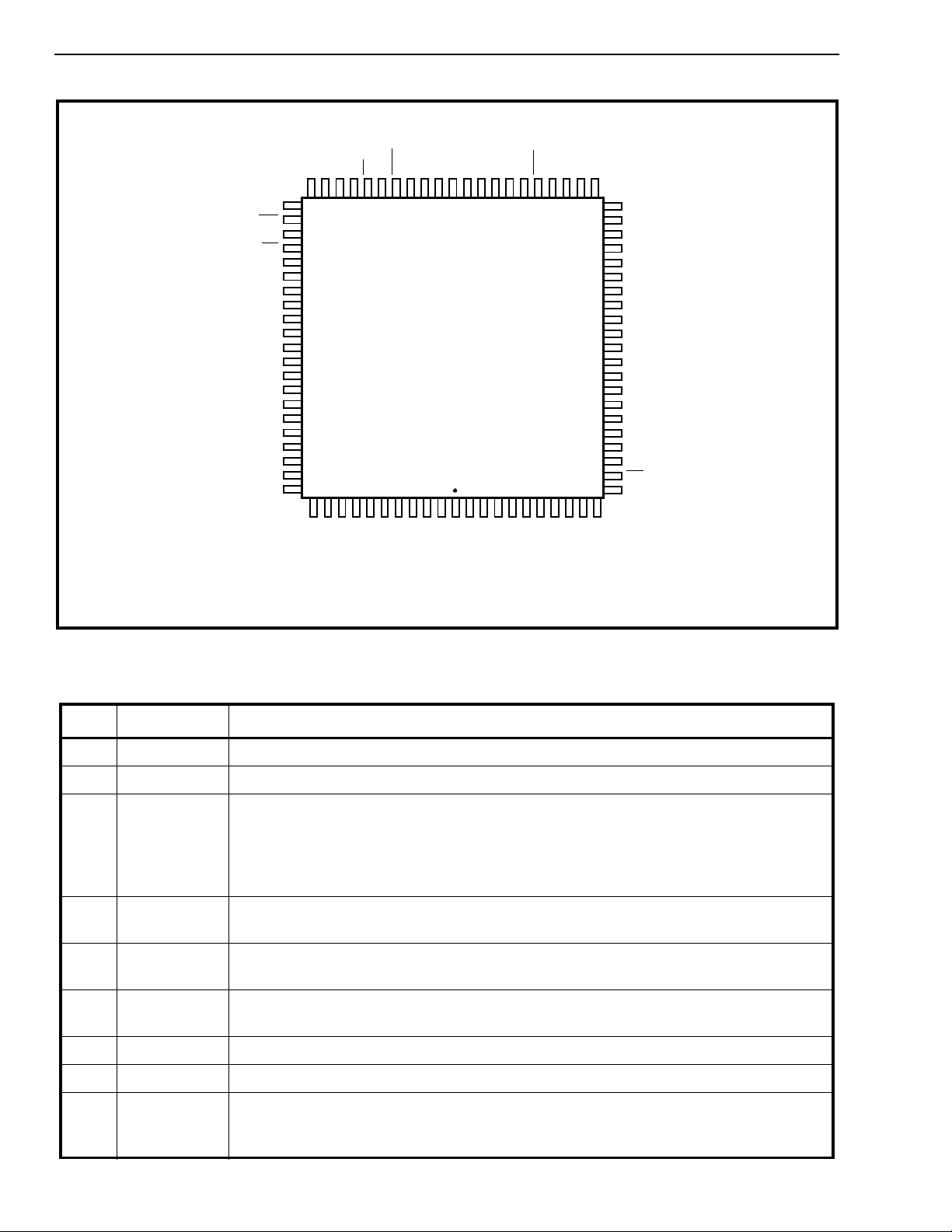
Figure 2 - Pin Connections
Pin Description
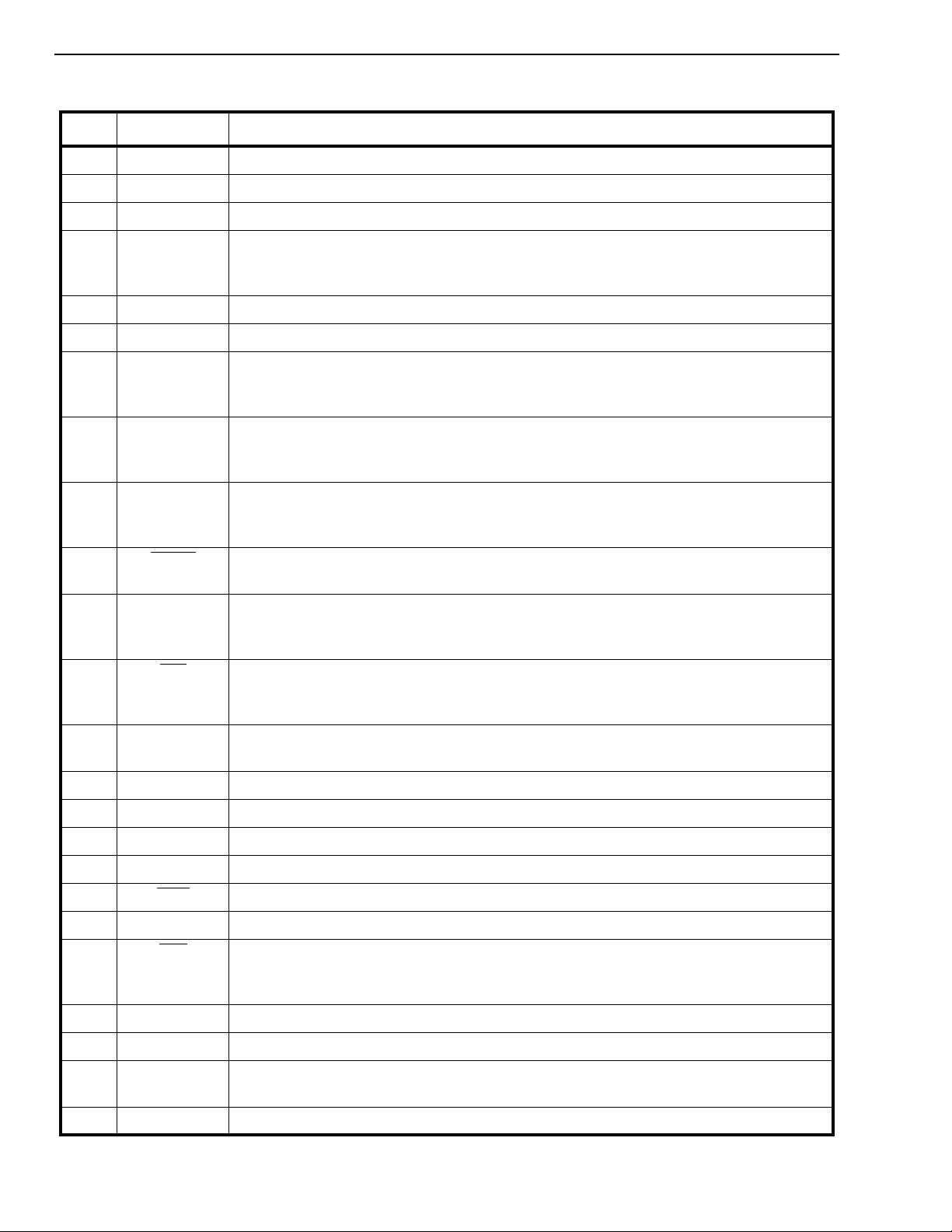
Pin # Name Description
1V
2V
SS
DD
3STo7Serial, 32 Channel , 2.048 Mb/s Lin k 7 (Outpu t Type 3). Only channels 9 - 31 are
4 DOUT8K0 Asynchron ou s 8 kHz Signal 0 (Outpu t Type 3). Sourced from the far-end DIN8K 0
5 DOUT8K1 Asynchron ou s 8 kHz Signal 1 (Outpu t Type 3). Sourced from the far-end DIN8K 1
6 C20o 20.48 MHz Clock (Output Type 3). Derived from transmit PLL 40.96 MHz clock divided
7NCNo Internal Connection.
8 FBADDR7 Frame Buffer RAM Addr ess Bit 7 (Outpu t Type 2).
9STo6ASerial, 32 Channel , 2.048 Mb/s Lin k 6A (Outpu t Type 3). Output is active only when
Power Supply Ground. Nominally 0 volts .
Positive Power Supply. Nominally 5 volts.
available for user data transfer (1.474 Mb/s). Channels 0 - 8 (0.576 Mb/ s) are reserved
for access to fiber overhead information. Output is active only when the receiver
detects the synchronization pattern on RxDA TA input stream; output is high impedance
during loss of synchronization.
input.
input.
by 2 (see pin 18). Made available for system use.
the receiver detects the synchronization pattern on RxDATA input stream; output is high
impedance during loss of synchronizat ion.
5-4

Preliminary Information MT90710
Pin Description
Pin # Name Description
10 STo5 Serial, 32 Channel, 2.048 Mb/s Lin k 5 (Outpu t Type 3). Output is active only when
the receiver detects the synchronization pattern on RxDATA input stream; output is high
impedance during loss of synchronizat ion.
11 V
12 V
DD
SS
13 C4o
Positive Po wer Supply. Nominally 5 volts.
Power Sup pl y Grou nd. Nominal ly 0 volts .
4.096 MHz Clock (Output Type 3). Used by the transmit PLL. This clock is the input
C40i (40.96MHz, see pin 18) master clock divided by 10 (inverted) and is fed back to
the external PLL circuit as a reference.
14 C4REF o 4.096 MHz Reference Cloc k (Ou tpu t Type 3). Used by transmit PLL. When in control-
ler mode this clock is derived from the system C4b
(4.096 MHz) clock input (see pin
57). When in peripheral mode this clock is extracted from the receive data on the fiber
port.
15,16,
NC No Internal Connection.
17
18 C40i Transmit 40.96 M H z Clock (In put Type 2). Derived from the transmit PL L. This is the
master clock used by the device.
19 STi1 Seri al , 32 Channel , 2.048 M b/s Lin k 1 (Inp ut Type 1).
20 STi2 Seri al , 32 Channel , 2.048 M b/s Lin k 2 (Inp ut Type 1).
21 V
22 V
SS
DD
Power Sup pl y Grou nd. Nominal ly 0 volts .
Positive Po wer Supply. Nominally 5 volts.
23 STi3 Seri al , 32 Channel , 2.048 M b/s Lin k 3 (Inp ut Type 1).
24 STi4 Seri al , 32 Channel , 2.048 M b/s Lin k 4 (Inp ut Type 1).
25 STi5 Seri al , 32 Channel , 2.048 M b/s Lin k 5 (Inp ut Type 1).
26 STi6A Serial, 32 Channel , 2.048 Mb/s Lin k 6A (Input Type 1).
27 STi6B Serial, 32 Channel , 2.048 Mb/s Lin k 6B (Input Type 1).
28 STi7 Seri al , 32 Channel , 2.048 M b/s Lin k 7 (Inp ut Type 1). Only channels 9 - 31 are avail-
able for user data transfer (1.47 2 Mb/s ). Data input on channel s 0 - 8 (0.576 Mb/s) is
ignored by the device. This bandwidth is reserved for fiber overhead information.
29 E20i Receiver 20.96 MHz Clock (Input Type 2). Extracted clo ck from the receive data
stream. Divided internally by 5 and phase corrected to frame synch pattern to produce
internal 2.048 MHz data clock for parsing the receive STi streams.
30 NC No Internal Connection.
31 V
SS
Power Sup pl y Grou nd. Nominal ly 0 volts .
32 NC No Internal Connection.
33 V
DD
Positive Po wer Supply. Nominally 5 volts.
34 NC No Internal Connection.
35 RxDATA Re ceiv e 4B/5B, NRZI Enc ode d Seria l Data (Input Type 1).
36 RLED " Rem o te Sync" LED Driver (Op en Col lector, Output Type 3). Drives the "Remote
Sync" LED on/off at approxi mately a 4 Hz rate when the remote interface is not syn-
chronized. Active only when the local interface is synchronized.
37 FBOE
Frame Buffer Ram Enab le (Ou tput Type 2). Generates a low going strobe during
valid RAM read access.
5-5

MT90710 Preliminary Information
Pin Description
Pin # Name Description
38 MODE2 Operatin g Mode Sele ct 2 (Input Type 1). See Table 1.
39 MODE1 Operatin g Mode S ele ct 1 (Inpu t Type 1). See Table 1.
40 MODE0 Operatin g Mode Sele ct 0 (Input Type 1). See Table 1.
41 STo0 Serial, 32 Channel, 2.048 Mb/s link 0 (O utput Type 3). Output is active only when
receiver detects the synchronization pattern on RxDATA input stream; output is high
impedance during loss of synchronizat ion.
42 V
43 V
DD
SS
Positive Power Supply. Nominally 5 volts.
Power Supply Ground. Nominally 0 volts .
44 STo2 Serial, 32 Channel, 2.048 Mb/s link 2 (O utput Type 3). Output active only when
receiver detects the synchronization pattern on RxDATA input stream; high impedance
output during loss of synchronization.
45 STo3 Serial, 32 Channel, 2.048 Mb/s link 3 (O utput Type 3). Output active only when
receiver detects the synchronization pattern on RxDATA input stream; high impedance
output during loss of synchronization.
46 STo4 Serial, 32 Channel, 2.048 Mb/s link 4 (O utput Type 3). Output active only when
receiver detects the synchronization pattern on RxDATA input stream; high impedance
output during loss of synchronization.
47 FBWE
Frame Buffer RAM Write Enable (Outpu t Type 2). Generates a low going strobe dur-
ing valid RAM write access.
48 STo1 Serial, 32 Channel, 2.048 Mb/s link 1 (O utput Type 3). Output active only when
receiver detects the synchronization pattern on RxDATA input stream; high impedance
output during loss of synchronization.
49 F0 b
System 8 kHz Reference Frame Pulse (Bi-directi on al; I npu t and Outpu t Types 3).
When in controller mode this is an input accepting the system referen ce pulse. In
peripheral mode this is an output supplying the system an 8 kHz reference frame pulse.
50 DOUT32K Asynchronous 32 kHz Signal 1 (Open Collector, Output Type 3). Sourced from the
far-end DIN32K input.
51 TxDATA Transmit 4B/5B, NRZI Encoded Serial Data (Output Type 3).
52 V
SS
Power Supply Ground. Nominally 0 volts .
53 IC Internally Connected (Output Type 1). Drives continuous logic 1. Leave open circuit.
54 V
DD
55 POR
Positive Power Supply. Nominally 5 volts.
Power On Reset (Input Type 2). Active low.
56 FBDATA 7 Frame Buffer Data Bit 7 (Bidirectional; Input Type 1 and Output Type 2). Data bit 7.
57 C4b
4.096 MHz Reference Clock (Bidirecti on al; Inpu t and Outp ut Types 3). Input used
by PLL in controller mode and derived from the system. In peripheral mod e this is an
output supplying the system 4. 096 MH z reference cloc k.
58 FBDATA 6 Frame Buffer Data Bit 6 (Bidirectional; Input Type 1 and Output Type 2). Data bit 6.
59 FBDATA5 Frame Buffer Data Bit 5 (Bidirectional; Input Type 1 and Output Type 2). Data bit 5.
60 DIN8K0 Asynchronous 8 kHz Signal 0 (Input Type 1). Transmitted to the far-end DOUT8K0
output.
61 FBDATA 4 Frame Buffer Data Bit 4 (Bidirectional; Input Type 1 and Output Type 2). Data bit 4.
5-6
 Loading...