MITEL MT9041BP Datasheet

MT9041B
T1/E1 System Synchronizer
Advance Information
Features
• Supports AT&T TR62411 and Bellcore
GR-1244-CORE Stratum 4 Enhanced and
Stratum 4 timing for DS1 Interfaces
• Supports ETSI ETS 300 011, TBR 4, TBR 12
and TBR 13 timing for E1 Interfaces
• Selectable 1.544MHz, 2.048MHz or 8kHz input
reference signals
• Provides C1.5, C2, C3, C4, C8 and C16 output
clock signals
• Provides 3 different styles of 8 KHz framing
pulses
• Attenuates wander from 1.9 Hz
Applications
• Synchronization and timing control for
multitrunk T1 and E1 systems
• ST-BUS clock and frame pulse sources
DS5059 ISSUE 3 Septemner 1999
Ordering Information
MT9041BP 28 Pin PLCC
-40 to +85 °C
Description
The MT9041B T1/E1 System Synchronizer contains
a digital phase-locked loop (DPLL), which provides
timing and synchronization signals for multitrunk T1
and E1 primary rate transmission links.
The MT9041B generates ST-BUS clock and framing
signals that are phase locked to either a 2.048MHz,
1.544MHz, or 8kHz input reference.
The MT9041B is compliant with AT&T TR62411 and
Bellcore GR-1244-CORE Stratum 4 Enhanced,
Stratum 4, and ETSI ETS 300 011. It will meet the
jitter tolerance, jitter transfer, intrinsic jitter, frequency
accuracy, capture range and phase change slope
requirements for these specifications.
REF
VDD VSS
Phase
Detector
Mode Select
Loop
Filter
MS FS1 FS2RST
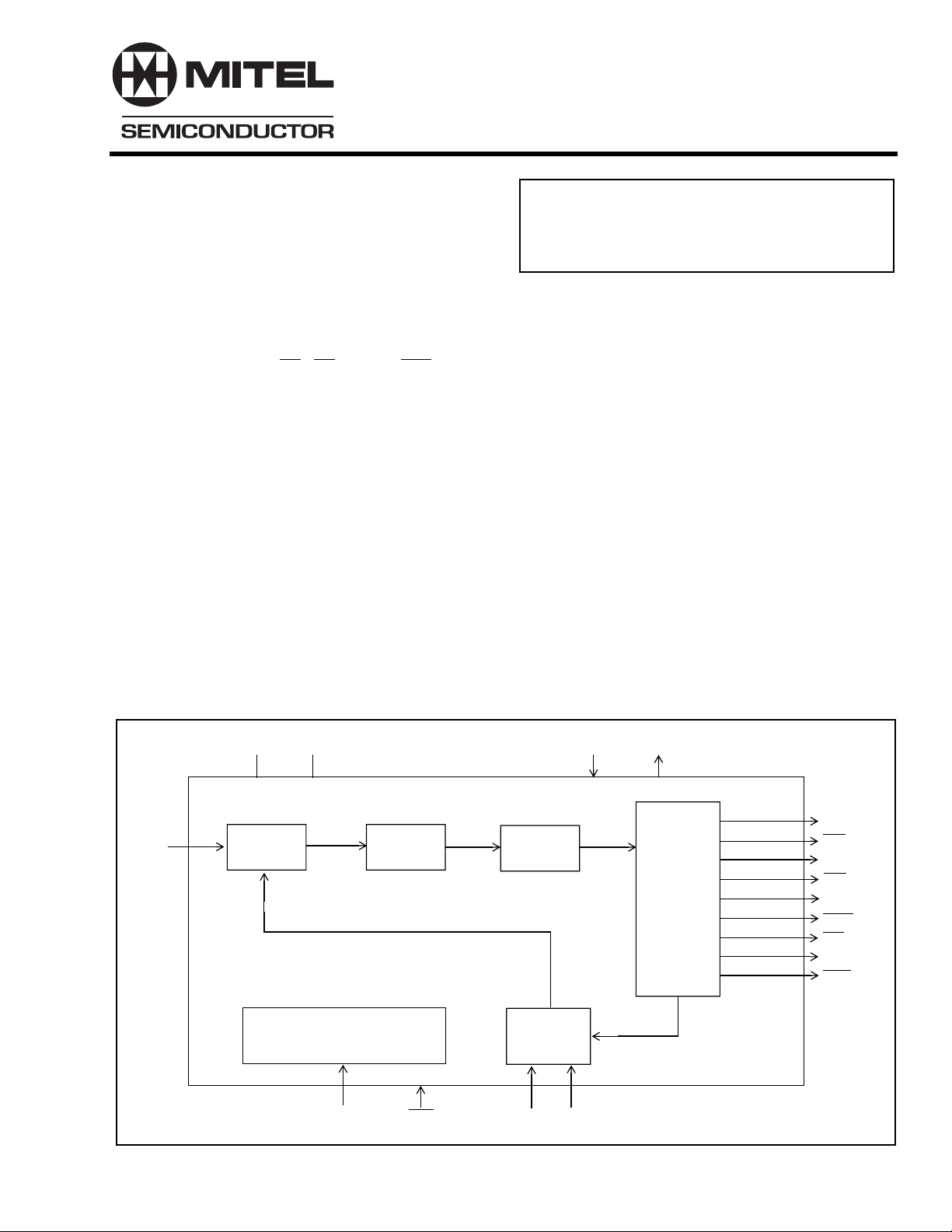
Figure 1 - Functional Block Diagram
DCO
Divider
OSCi OSCo
Output
Interface
Circuit
C1.5o
C3o
C2o
C4o
C8o
C16o
F0o
F8o
F16o
1

MT9041B Advance Information
VSS
IC0
NC
REF
RST
FS1
FS2
VSS
C8o
262728
25
IC0
24
IC0
23
MS
22
IC0
21
IC0
20
IC1
IC0
19
VDD
C16o
VDD
OSCo
OSCi
F16o
F0o
F8o
C1.5o
MT9041B
C2o
C3o
1
C4o
432
5
6
7
8
9
10
11
12 13 14 15 16 17 18
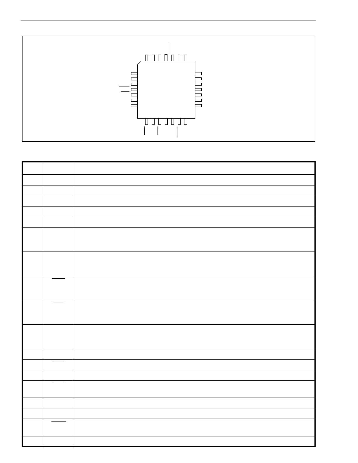
Figure 2 - Pin Connections
Pin Description
Pin # Name Description
1VSSGround. 0 Volts.
2 IC0 Internal Connect. Connect to Vss
3 NC No Connect. Connect to Vss
4 REF Reference (TTL Input). PLL reference clock.
5 V
6 OSCo Oscillator Master Clock (CMOS Output). For crystal operation, a 20MHz crystal is
Positive Supply Voltage. +5VDC nominal.
DD
connected from this pin to OSCi, see Figure 6. For clock oscillator operation, this pin is left
unconnected, see Figure 5.
7 OSCi Oscillator Master Clock (CMOS Input). For crystal operation, a 20MHz crystal is
connected from this pin to OSCo, see Figure 6. For clock oscillator operation, this pin is
connected to a clock source, see Figure 5.
8 F16o Frame Pulse ST-BUS 16.384Mb/s (CMO7S Output). This is an 8kHz 61ns active low
framing pulse, which marks the beginning of an ST-BUS frame. This is typically used for
ST-BUS operation at 16.384Mb/s. See Figure 11.
9 F0o Frame Pulse ST-BUS 2.048Mb/s (CMOS Output). This is an 8kHz 244ns active low
framing pulse, which marks the beginning of an ST-BUS frame. This is typically used for
ST-BUS operation at 2.048Mb/s and 4.096Mb/s. See Figure 11.
10 F8o Frame Pulse ST-BUS 8.192Mb/s (CMOS Output). This is an 8kHz 122ns active high
framing pulse, which marks the beginning of an ST-BUS frame. This is used for ST-BUS
operation at 8.192Mb/s. See Figure 11.
11 C1.5o Clock 1.544MHz (CMOS Output). This output is used in T1 applications.
12 C3o Clock 3.088MHz (CMOS Output). This optional output is used in T1 applications.
13 C2o Clock 2.048MHz (CMOS Output). This output is used for ST-BUS operation at 2.048Mb/s.
14 C4o Clock 4.096MHz (CMOS Output). This output is used for ST-BUS operation at 2.048Mb/s
and 4.096Mb/s.
15 V
Ground. 0 Volts.
SS
16 C8o Clock 8.192MHz (CMOS Output). This output is used for ST-BUS operation at 8.192Mb/s.
17 C16o Clock 16.384MHz (CMOS Output). This output is used for ST-BUS operation at 16.384Mb/
s.
18 V
2
Positive Supply Voltage. +5VDC nominal.
DD

Advance Information MT9041B
Pin Description (continued)
Pin # Name Description
19 IC0 Internal Connect. Connect to Vss
20 IC1 Internal Connect. Leave open Circuit
21 IC0 Internal Connect. Connect to Vss
22 IC0 Internal Connect. Connect to Vss
23 MS Mode/Control Select (TTL Input). This pin, determines the device’s state (Normal, or
Freerun) of operation. The logic level at this input is gated in by the rising edge of F8o. See
Table 3.
24 IC0 Internal Connect. Connect to Vss
25 IC0 Internal Connect. Connect to Vss
26 FS2 Frequency Select 2 (TTL Input). This input, in conjunction with FS1, selects which of three
possible frequencies (8kHz, 1.544MHz, or 2.048MHz) may be input to the REF input. See
Table 1.
27 FS1 Frequency Select 1 (TTL Input). See pin description for FS2.
28 RST Reset (Schmitt Input). A logic low at this input resets the MT9041B. To ensure proper
operation, the device must be reset after reference signal frequency changes and power-up.
The RST pin should be held low for a minimum of 300ns. While the RST pin is low, all frame
and clock outputs are at logic high. Following a reset, the input reference source and output
clocks and frame pulses are phase aligned as shown in Figure 10.
Functional Description
The MT9041B is a System Synchronizer, providing
timing (clock) and synchronization (frame) signals to
interface circuits for T1 and E1 Primary Rate Digital
Transmission links.
Figure 1 is a functional block diagram which is
described in the following sections.
Frequency Select MUX Circuit
The MT9041B operates on the falling edges of one
of three possible input reference frequencies (8kHz,
1.544MHz or 2.048MHz). The frequency select
inputs (FS1 and FS2) determine which of the three
frequencies may be used at the reference input
(REF). A reset (RST) must be performed after every
frequency select input change. Operation with FS1
and FS2 both at logic low is reserved and must not
be used. See Table 1.
FS2 FS1 Input Frequency
0 0 Reserved
0 1 8kHz
1 0 1.544MHz
1 1 2.048MHz
Table 1 - Input Frequency Selection
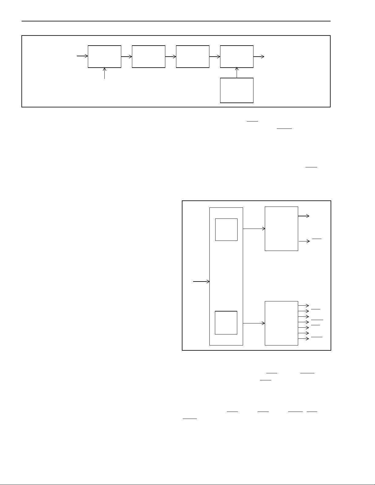
Digital Phase Lock Loop (DPLL)
The DPLL of the MT9041B consists of a Phase
Detector, Limiter, Loop Filter, Digitally Controlled
Oscillator, and a Control Circuit (see Figure 3).
Phase Detector - the Phase Detector compares the
primary reference signal (REF) with the feedback
signal from the Frequency Select MUX circuit, and
provides an error signal corresponding to the phase
difference between the two. This error signal is
passed to the Limiter circuit. The Frequency Select
MUX allows the proper feedback signal to be
externally selected (e.g., 8kHz, 1.544MHz or
2.048MHz).
Limiter - the Limiter receives the error signal from
the Phase Detector and ensures that the DPLL
responds to all input transient conditions with a
maximum output phase slope of 5ns per 125us. This
3

MT9041B Advance Information
REF Reference
Frequency Select MUX
Phase
Detector
Feedback Signal
from
Limiter Loop Filter
Figure 3 - DPLL Block Diagram
is well within the maximum phase slope of 7.6ns per
125us or 81ns per 1.326ms specified by Bellcore
GR-1244-CORE Stratum 4E.
Loop Filter - the Loop Filter is similar to a first order
low pass filter with a 1.9 Hz cutoff frequency for all
three reference frequency selections (8kHz,
1.544MHz or 2.048MHz). This filter ensures that the
jitter transfer requirements in ETS 300 011 and AT&T
TR62411 are met.
Control Circuit - the Control Circuit sets the mode
of the DPLL. The two possible modes are Normal
and Freerun.
Digitally Controlled Oscillator (DCO) - the DCO
receives the limited and filtered signal from the Loop
FIlter, and based on its value, generates a
corresponding digital output signal. The
synchronization method of the DCO is dependent on
the state of the MT9041B.
Digitally
Controlled
Oscillator
Control
Circuit
DPLL Reference
to
Output Interface Circuit
outputs. The C8o, C4o and C2o clocks are
generated by simply dividing the C16o clock by two,
four and eight respectively. These outputs have a
nominal 50% duty cycle.
The T1 Divider Circuit uses the 12.384MHz signal to
generate two clock outputs. C1.5o and C3o are
generated by dividing the internal C12 clock by four
and eight respectively. These outputs have a nominal
50% duty cycle.
C1.5o
C3o
From
DPLL
Tapped
Delay
Line
12MHz
T1 Divider
In Normal Mode, the DCO provides an output signal
which is frequency and phase locked to the selected
input reference signal.
In Freerun Mode, the DCO is free running with an
accuracy equal to the accuracy of the OSCi 20MHz
source.
Output Interface Circuit
The output of the DCO (DPLL) is used by the Output
Interface Circuit to provide the output signals shown
in Figure 4. The Output Interface Circuit uses two
Tapped Delay Lines followed by a T1 Divider Circuit
and an E1 Divider Circuit to generate the required
output signals.
Two tapped delay lines are used to generate a
16.384MHz and a 12.352MHz signals.
The E1 Divider Circuit uses the 16.384MHz signal to
generate four clock outputs and three frame pulse
C2o
C4o
C8o
C16o
F0o
F8o
F16o
Tapped
Delay
Line
E1 Divider
16MHz
Figure 4 - Output Interface Circuit Block
Diagram
The frame pulse outputs (F0o, F8o, F16o) are
generated directly from the C16 clock.
The T1 and E1 signals are generated from a
common DPLL signal. Consequently, the clock
outputs C1.5o, C3o, C2o, C4o, C8o, C16o, F0o and
F16o are locked to one another for all operating
states, and are also locked to the selected input
reference in Normal Mode. See Figures 11 and 12.
4

Advance Information MT9041B
All frame pulse and clock outputs hav e limited driving
capability, and should be buffered when driving high
capacitance (e.g. 30pF) loads.
Master Clock
The MT9041B can use either a clock or crystal as
the master timing source. For recommended master
timing circuits, see the Applications - Master Clock
section.
Control and Modes of Operation
The MT9041B can operate either in Normal or
Freerun modes.
As shown in Table 2, pin MS selects between
NORMAL and FREERUN modes.
MS Description of Operation
0 NORMAL
1 FREERUN
Table 2 - Operating Modes
Freerun Mode
Freerun Mode is typically used when a master clock
source is required, or immediately following system
power-up before network synchronization is
achieved.
In Freerun Mode, the MT9041B provides timing and
synchronization signals which are based on the
master clock frequency (OSCi) only, and are not
synchronized to the reference signal (REF).
The accuracy of the output clock is equal to the
accuracy of the master clock (OSCi). So if a ±32ppm
output clock is required, the master clock must also
be ±32ppm. See Applications - Crystal and Clock
Oscillator sections.
MT9041B Measures of Performance
The following are some synchronizer performance
indicators and their corresponding definitions.
Intrinsic Jitter
Normal Mode
Normal Mode is typically used when a slave clock
source synchronized to the network is required.
In Normal Mode, the MT9041B provides timing
(C1.5o, C2o, C3o, C4o, C8o and C16o) and frame
synchronization (F0o, F8o, F16o) signals, which are
synchronized to reference input (REF). The input
reference signal may have a nominal frequency of
8kHz, 1.544MHz or 2.048MHz.
From a reset condition, the MT9041B will take up to
25 seconds for the output signal to be phase locked
to the reference.
The reference frequencies are selected by the
frequency control pins FS2 and FS1 as shown in
Table 1.
Intrinsic jitter is the jitter produced by the
synchronizing circuit and is measured at its output. It
is measured by applying a reference signal with no
jitter to the input of the device, and measuring its
output jitter. Intrinsic jitter may also be measured
when the device is in a non-synchronizing mode, i.e.
free running mode, by measuring the output jitter of
the device. Intrinsic jitter is usually measured with
various bandlimiting filters depending on the
applicable standards.
Jitter Tolerance
Jitter tolerance is a measure of the ability of a PLL to
operate properly (i.e., remain in lock and or regain
lock), in the presence of large jitter magnitudes at
various jitter frequencies applied to its reference.
The applied jitter magnitude and jitter frequency
depends on the applicable standards.
Jitter Transfer
Jitter transfer or jitter attenuation refers to the
magnitude of jitter at the output of a device for a
given amount of jitter at the input of the device. Input
jitter is applied at various amplitudes and
frequencies, and output jitter is measured with
various filters depending on the applicable
standards.
5

MT9041B Advance Information
For the MT9041B, two internal elements determine
the jitter attenuation. This includes the internal 1.9Hz
low pass loop filter and the phase slope limiter. The
phase slope limiter limits the output phase slope to
5ns/125us. Therefore, if the input signal exceeds this
rate, such as for very large amplitude low frequency
input jitter, the maximum output phase slope will be
limited (i.e., attenuated) to 5ns/125us.
The MT9041B has nine outputs with three possible
input frequencies for a total of 27 possible jitter
transfer functions. However, the data sheet section
on AC Electrical Characteristics - Jitter Transfer
specifies transfer values for only three cases, 8kHz
to 8kHz, 1.544MHz to 1.544MHz and 2.048MHz to
2.048MHz. Since all outputs are derived from the
same signal, these transfer values apply to all
outputs.
It should be noted that 1UI at 1.544MHz is 644ns,
which is not equal to 1UI at 2.048MHz, which is
488ns. Consequently, a transfer value using different
input and output frequencies must be calculated in
common units (e.g. seconds) as shown in the
following example.
What is the T1 and E1 output jitter when the T1 input
jitter is 20UI (T1 UI Units) and the T1 to T1 jitter
attenuation is 18dB?
usually made with large input jitter signals (e.g. 75%
of the specified maximum jitter tolerance).
Frequency Accuracy
Frequency accuracy is defined as the absolute
tolerance of an output clock signal when it is not
locked to an external reference, but is operating in a
free running mode. For the MT9041B, the Freerun
accuracy is equal to the Master Clock (OSCi)
accuracy.
Capture Range
Also referred to as pull-in range. This is the input
frequency range over which the synchronizer must
be able to pull into synchronization. The MT9041B
capture range is equal to ±230ppm minus the
accuracy of the master clock (OSCi). For example, a
±32ppm master clock results in a capture range of
±198ppm.
Lock Range
This is the input frequency range over which the
synchronizer must be able to maintain
synchronization. The lock range is equal to the
capture range for the MT9041B.
A–
------ -
OutputT 1 InputT1
OutputT 120
OutputE1 OutputT1
OutputE1 OutputT1
Using the above method, the jitter attenuation can be
calculated for all combinations of inputs and outputs
based on the three jitter transfer functions provided.
Note that the resulting jitter transfer functions for all
combinations of inputs (8kHz, 1.544MHz, 2.048MHz)
and outputs (8kHz, 1.544MHz, 2.048MHz,
4.096MHz, 8.192MHz, 16.384MHz) for a given input
signal (jitter frequency and jitter amplitude) are the
same.
Since intrinsic jitter is always present, jitter
attenuation will appear to be lower for small input
jitter signals than for large ones. Consequently,
accurate jitter transfer function measurements are
×10 2.5UI T 1()==
20
×10=
18–
-------- 20
1UIT1()
----------------------
×=
1UIE 1()
-------------------
644ns()
488ns()
3.3UI T 1()=×=
Phase Slope
Phase slope is measured in seconds per second and
is the rate at which a given signal changes phase
with respect to an ideal signal. The given signal is
typically the output signal. The ideal signal is of
constant frequency and is nominally equal to the
value of the final output signal or final input signal.
Phase Continuity
Phase continuity is the phase difference between a
given timing signal and an ideal timing signal at the
end of a particular observation period. Usually, the
given timing signal and the ideal timing signal are of
the same frequency. Phase continuity applies to the
output of the synchronizer after a signal disturbance
due to a reference switch or a mode change. The
observation period is usually the time from the
disturbance, to just after the synchronizer has settled
to a steady state.
In the case of the MT9041B, the output signal phase
continuity is maintained to within ±5ns at the
instance (over one frame) of mode changes. The
total phase shift may accumulate up to ±200ns over
6
 Loading...