MITEL MT8979AP, MT8979AC, MT8979AE Datasheet
ISO-CMOS ST-BUS FAMILY
MT8979
CEPT PCM 30/CRC-4 Framer & Interface
Features
• Single chip pr imary rate 20 48 kb it/s CEPT
transceiver with CRC-4 option
• Meets CCITT Recommendation G.704
• Selectable HDB3 or AMI line code
• Tx and Rx fr ame an d mult ifram e
synchronization signals
• Two frame elastic buffer with 32 µsec jitter
buffer
• Frame alignm ent an d CRC error coun ters
• Insertion and dete ction of A, B, C, D sign alling
bits with o ptiona l debo unce
• On-chip attenuation ROM with option for ADI
codecs
• Per channel , overa ll and remote loop aro und
• ST-BUS compatible
Applications
• Primary rate ISDN netw ork node s
• Multiplexing equipment
• Private network: PBX to PBX links
• High speed comp uter t o com pute r links
ISSUE 7 May 1995
Ordering Information
MT8979AC 28 Pin Cerami c DIP
MT8979A E 28 Pin Pl astic D IP
MT8979A P 44 Pin PLC C
-40° to 85°C
Descript io n
The MT8979 is a single chip CEPT digital trunk
transceiver that meets the requirements of CCITT
Recommendation G.704 for digital multiplex
equipment.
The MT8979 is fabricated in Mitel’s low power
ISO-CMOS technology.
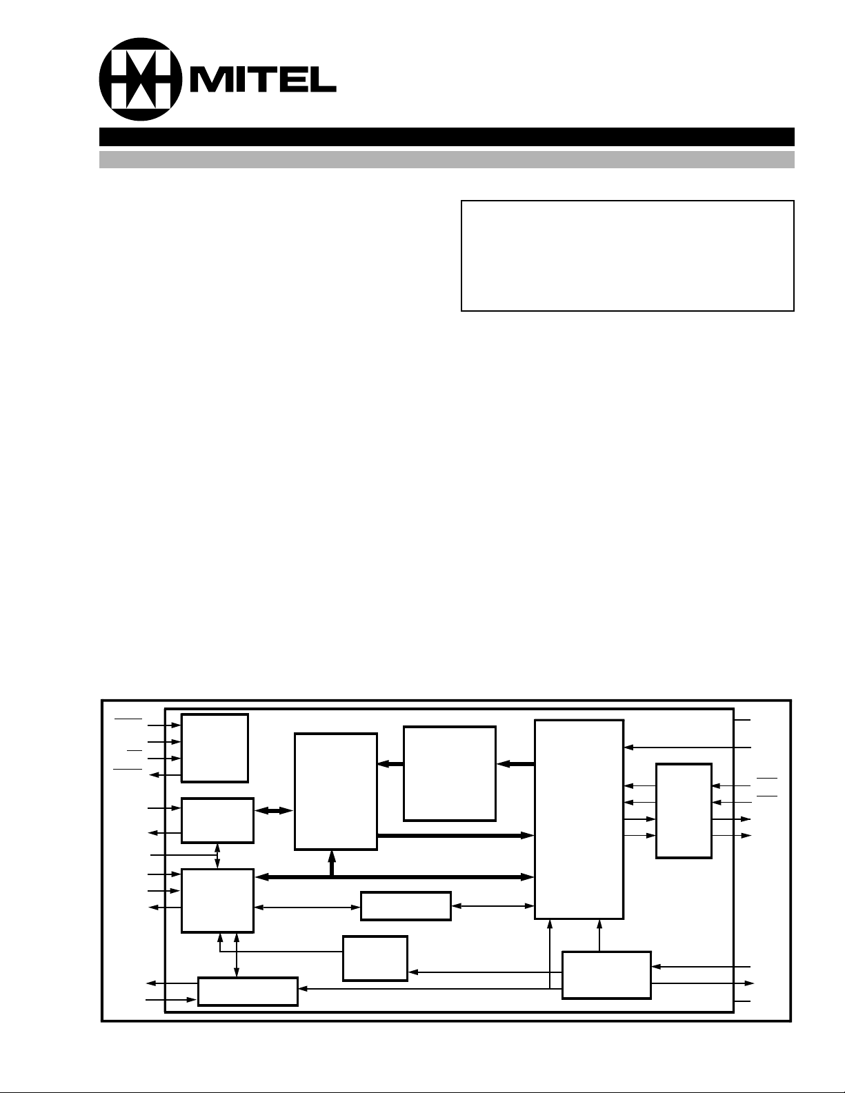
TxMF
C2i
F0i
RxMF
DSTi
DSTo
ADI
CSTi0
CSTi1
CSTo
XCtl
XSt
ST-BUS
Timing
Circuitry
PCM/Data
Interface
Serial
Control
Interface
Control Logic
2 Frame
Digital
Attenuator
ROM
ABCD Bit RAM
Phase
Detector
Elastic Buf fe r
with Slip
Control
Figure 1 - Functiona l Block Diagram
CEPT
Link
Interface
Counter
CEPT
Remote
&
Digital
Loopbacks
V
DD
RxD
RxA
RxB
TxA
TxB
E2i
E8Ko
V
SS
4-161
MT8979 ISO-CMOS
TxA
TxB
DSTo
NC
RxA
RxB
RxD
CSTi1
NC
NC
ADI
CSTi0
E8Ko
VSS
Pin Description
Pin #
Name Description
DIP PLCC
1
2
3
4
5
6
7
8
9
10
11
12
13
14
28 PIN CERDIP/PDIP
28
27
26
25
24
23
22
21
20
19
18
17
16
15
VDD
IC
F0i
E2i
NC
RxMF
TxMF
C2i
NC
DSTi
NC
CSTo
XSt
XCtl
NC
NC
RxA
RxB
RxD
NC
CSTi1
NC
NC
NC
ADI
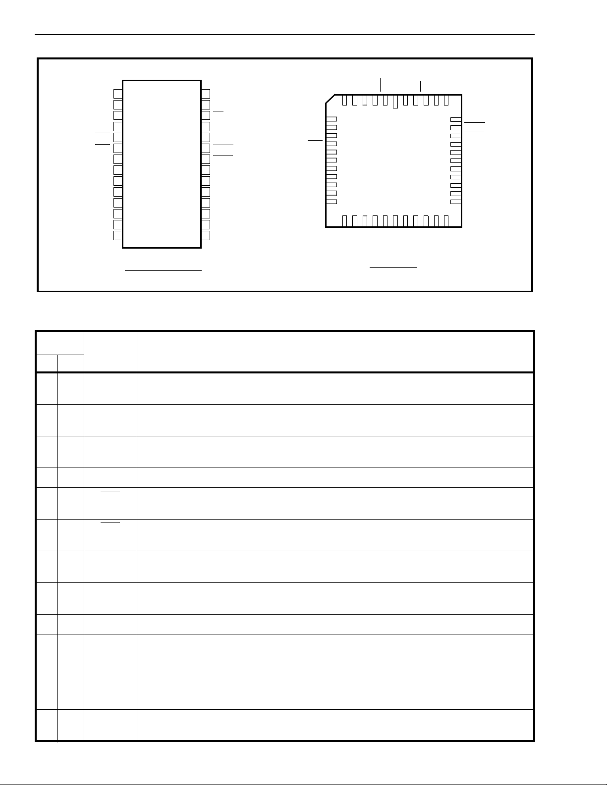
Figure 2 - Pin Connections
VSS
DSTo
NC
65432 44434241
7
8
9
10
11
12
13
14
15
16
17
VSS
E8Ko
CSTi0
VDD
TxB
TxA
ICNCF0iNCE2i
1
231819 2021 22 24252627 28
NC
44 PIN PLCC
VSS
XSt
XCtl
NC
CSTo
40
39
38
37
36
35
34
33
32
31
30
29
NC
NC
RxMF
TxMF
NC
NC
C2i
NC
NC
NC
NC
NC
DSTi
1 2 TxA Transmit A (Output): A split phase unipolar signal suita ble for use with TxB and an
external line driver and transformer to construct the bipolar line signal .
2 3 TxB Transmit B (Output:) A split phase unipolar signal suitabl e for use with TxA and an
external line driver and transformer to construct the bipolar line signal .
3 5 DSTo Data ST-BUS (Output): A 2048 kbit/s serial output stream which contains the 30 PCM or
data channels received from the CEPT line.
4 4 NC No Connecti on .
59 RxA
Receive A (Input): Received split phase unipolar signal decoded from a bipolar line
receiver.
610 RxB
Receive B (Input): Received split phase unipolar signal decoded from a bipolar line
receiver.
7 11 RxD Received Data (In put): Input of the unipolar data generat ed from the line receive r. This
data may be NRZ or RZ.
8 13 CSTi1 Control ST-BUS Inpu t #1: A 2048 kbit/s stre am that cont ains channel associated
signalling, frame alignment and diagnostic functions.
9 NC No Connecti on .
10 NC No Connecti on .
11 17 ADI Alternate Digit Inversion (Input): If this input is high, the CE PT timeslo ts which are
specified on CSTi0 as voice channels are ADI coded and decoded. When this bit is low it
disables ADI coding for all channels. This feature allows either ADI or non-ADI codecs to
be used on DSTi and DSTo.
12 19 CSTi0 Control ST-BUS Inpu t #0: A 2048 kbit/s stream that contai ns 30 per channel control
words and two Master Control Words.
4-162

Pin Description (Continued)
ISO-CMOS MT8979
Pin #
Name Description
DIP PLCC
13 20 E8Ko E xtracted 8 kHz Clock (Output): An 8 kHz output generated by dividing the extracted
2048 kHz clock by 256 and aligning it with the received CEPT frame. The 8 kHz signal
can be used for synchronizing the system clock to the extracted 2048 kHz clock. Only
valid when device achieves synchronization (goes low during a loss of signal or a loss
of basic frame synchronization condition).
E8Ko goes high impedance when 8kHzSEL = 0 in MCW2.
15 23 XCtl External Control (Output): An uncommitted external out put pin which is set or reset
via bit 1 in Master Cont rol Word 2 on CSTi0. The state of XCtl is updated once per
frame.
16 24 XSt Ext ernal Status: The state of this pin is sampled once per frame and the status is
reported in bit 1 of the Master Status Word 1 on CSTo.
17 26 CSTo Cont rol ST-BUS Output: A 2048 kbit /s serial control stream which provides the 16
signalling words, two Master Status Words, Phase Status Word and CRC Error Count.
18 NC No Connection .
19 28 DSTi D ata ST-BUS Input: This pin accepts a 2048 kbit/s serial stream which contains the
30 PCM or data channels to be transmitted on the CEPT trunk.
20 NC No Connection .
21 34 C2i 2048 kbit/s System Clock (Input): The master c lock for the S T-BUS s ection of th e
chip. All data on the ST-BUS is clocked in on the falling edge of the C2i and output on
the rising edge. The falling edge of C2i is also used to clock out data on the CEPT
transmit link.
22 37 TxMF
Transmit Multiframe Boundary (Input): This input can be used to set the channel
associated and CRC transmitted multiframe boundary (clear the frame counters). The
device will generate its own multiframe if this pin is held high.
23 38 RxMF
Received Multiframe Boundary (Output): An output pulse delimiting the received
Multiframe boundary. (This multiframe is not related to the received CRC multiframe.)
The next frame output on the data stream (DSTo) is received as frame 0 on the CEPT
link.
24 NC No Connection .
25 40 E2i Extracted 2048 kHz Clock (Input): The falling edge of this 2048 kHz clock is used to
latch the received data (RxD). This clock input must be derived from the CEPT
received data and must have its falling edge aligned with the center of the received bit
(RxD).
26 42 F0i
Frame Pulse Input: The ST-BUS frame synchronization signal which defines the
beginning of the 32 channel frame.
27 44 IC Internal Connection: Tie to V
28 1 V
DD
Positive Power Supply Input (+5 Volts).
(Ground) for normal operation.
SS
14 6,8,
22
V
SS
Negative Power Supply Input (Ground).
4-163
MT8979 ISO-CMOS
Functional Description
The MT8979 is a CEPT trunk digital link interface
conforming to CCITT Recommendation G.704 for
PCM 30 and I.431 for ISDN. It includes features
such as: insertion and detection of synchronization
patterns, optional cyclical redundancy check and far
end error performance reporting, HDB3 decoding
and optional coding, channel associated or common
channel signalling, programmable digital attenuation
and a two frame received elastic buffer. The
MT8979 can also monitor several conditions on the
CEPT digital trunk, which include, frame and
multiframe synchronization, received all 1’s alarms,
data slips as well as framing and CRC errors, both
near and far end.
The system interface to the MT8979 is a TDM bus
structure that operates at 2048 kbit/s known as the
ST-BUS. This serial stream is divided into 125 µs
frames that are made up of 32 x 8 bit channels.
The line interface to the MT8979 consists of split
phase unipolar inputs and outputs which are
supplied from/to a bipolar line receiver/driver,
respectively.
CEPT Interface
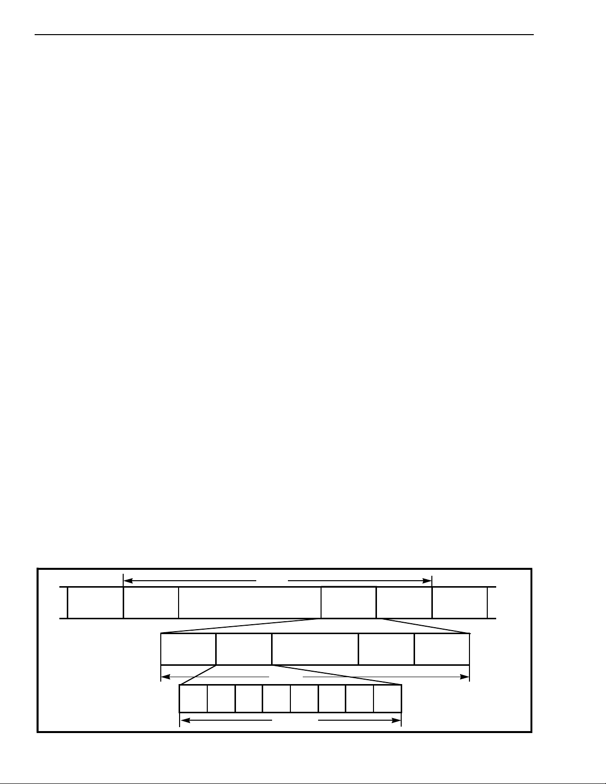
The CEPT frame format consists of 32, 8 bit
timeslots. Of the 32 timeslots in a frame, 30 are
defined as information channels, timeslots 1-15 and
17-31 which correspond to telephone channels 1-30.
An additional voice/data channel may be obtained by
placing the device in common channel signalling
mode. This allows use of timeslot 16 for 64 kbit/s
common channel signalling.
Synchronization is included within the CEPT bit
stream in the form of a bit pattern inserted into
timeslot 0. The contents of timeslot 0 alternate
between the frame alignm ent pattern and the
non-frame alignment pattern as described in Figure
4. Bit 1 of the frame alignment and non-frame
alignment bytes have provisions for additional
protection against false synchronization or enhanced
error monitoring. This is described in more detail in
the following section.
In order to accomplish multiframe synchronization, a
16 frame multiframe is defined by sending four zeros
in the high order quartet of timeslot 16 frame 0, i.e.,
once every 16 frames (see Figure 5). The CEPT
format has four signalling bits, A, B, C and D.
Signalling bits for all 30 information channels are
transmitted in timeslot 16 of frames 1 to 15. These
timeslots are subdivided into two quartets (see Table
6).
Cyclic Redundancy Check (CRC)
An optional cyclic redundancy check (CRC) has
been incorporated within CEPT bit stream to provide
additional protection against simulation of the frame
alignment signal, and/or where there is a need for an
enhanced error monitoring capability. The CRC
process treats the binary string of ones and zeros
contained in a submultiframe (with CRC bits set to
binary zero) as a single long binary number. This
string of data is first multiplied by x
the generating polynomial x
4
then divided by
4
+x+1. This division
process takes place at both the transmitter and
receiver end of the link. The remainder calculated at
the receiver is compared to the one received with the
data over the link. If they are the same, it is of high
probability that the previous submultiframe was
received error free.
The CRC procedure is based on a 16 frame
multiframe, which is divided into two 8 frame
submultiframes (SMF). The frames which contain
the frame alignment pattern contain the CRC bits, C
to C4 respectively, in the bit 1 position. The frames
1
4-164
2.0 ms
Frame
15 0 14 15 0
Timeslot
Most
Significant
Bit (First)
••••••••
0 1 30 31
Bit
12345678
Timeslot Timeslot Timeslot
Bit Bit Bit Bit Bit BitBit
••••
125 µs
Least
Significant
Bit (Last)
(8/2.048) µs
Figure 3 - CEPT Link Frame & Multiframe Format
FrameFrameFrameFrame
ISO-CMOS MT8979
which contain the non-frame alignment pattern
contain within the bit 1 position, a 6 bit CRC
multiframe alignment signal and two spare bits (in
frames 13 and 15), which are used for CRC error
performance reporting (refer to Figure 6). During the
CRC encoding procedure the CRC bit positions are
initially set at zero. The remainder of the calculation
is stored and inserted into the respective CRC bits of
the next SMF. The decoding process repeats the
multiplication division process and compares the
remainder with the CRC bits received in the next
SMF.
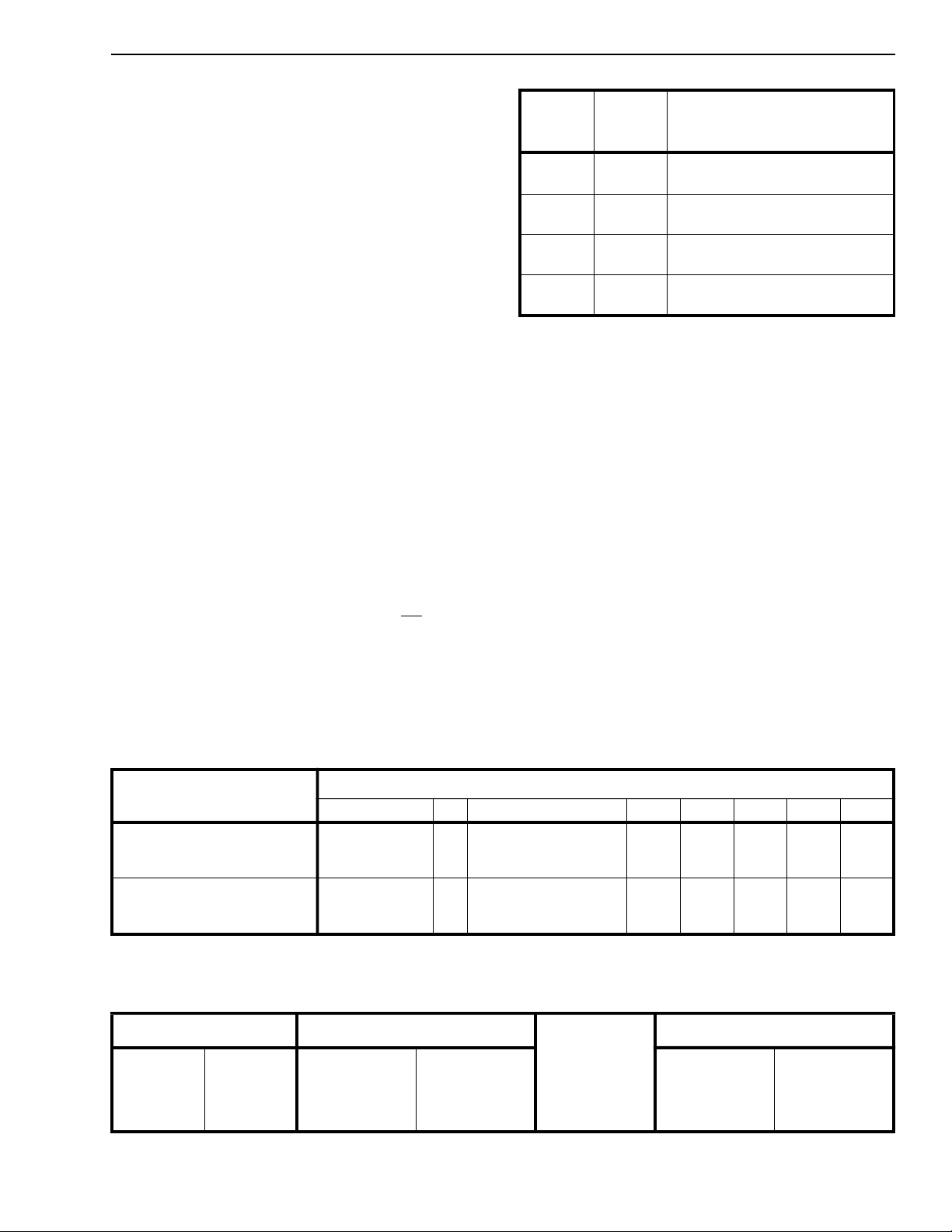
The two spare bits (denoted Si1 and Si2 in Figure 6)
in the CRC-4 multiframe are used to monitor far-end
error performance. The results of the CRC-4
comparisons for the previously received SMFII and
SMFI are encoded and transmitted back to the far
end in the Si bits (refer to Table 1).
ST-BUS Interfac e
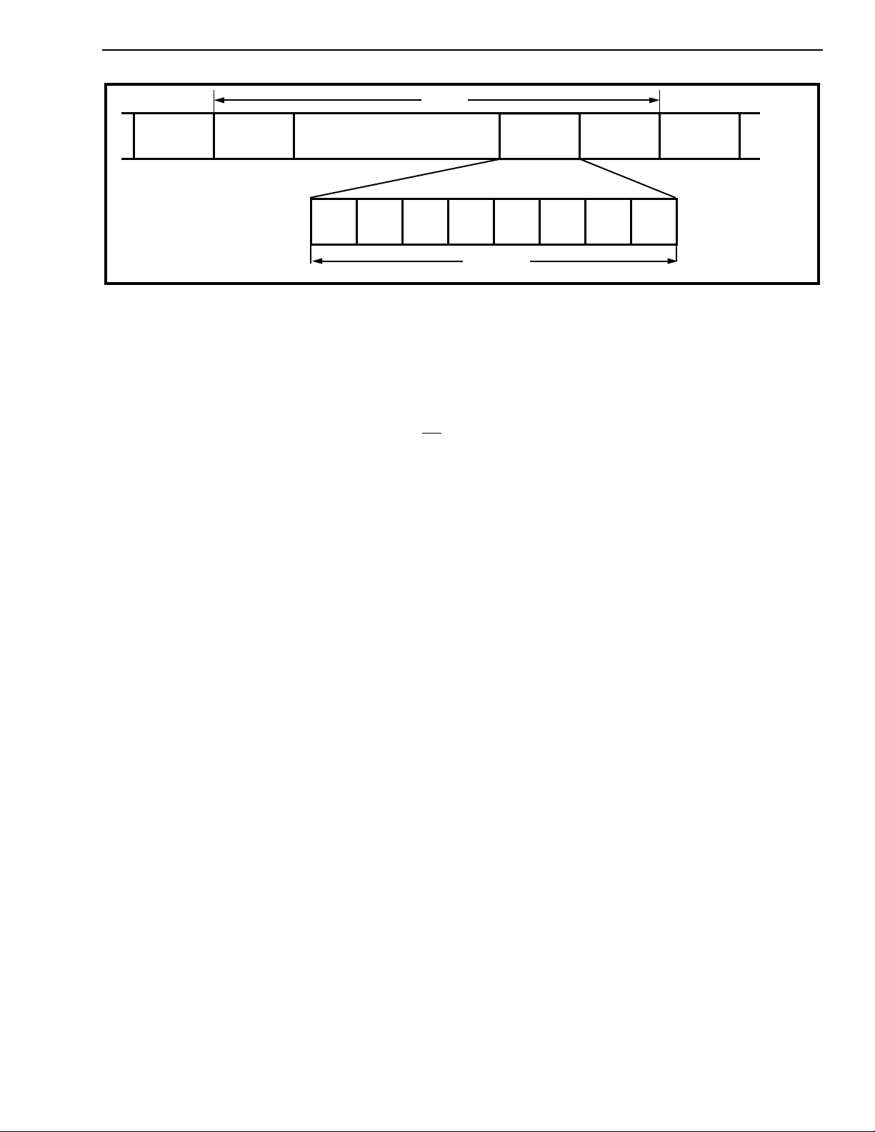
The ST-BUS is a synchronous time division
multiplexed serial bus with data streams operating at
2048 kbit/s and configured as 32, 64 kbit/s channels
(refer Figure 7). Synchronization of the dat a transfer
is provided from a frame pulse, which identifies the
frame boundaries and repeats at an 8 kHz rate.
Figure 17 shows how the frame pulse (F0i
the ST-BUS frame boundaries. All data is clocked
into the device on the falling edge of the 2048 kbit/s
clock (C2i), while data is clocked out on the rising
edge of the 2048 kbit/s clock at the start of the bit
cell.
) defines
Si1 bit
(frame
13)
11
10
01
00
Si2 bit
(frame
15)
Meaning
CRC results for both SMFI, II a re
error free.
CRC result for SMFII is in error.
CRC result for SMFI is error free.
CRC result for S MFII is erro r fre e.
CRC result for SMFI is in error.
CRC results for both SMFI, II a re
in error.
Table 1. Coding of Spare Bits Si1 and Si2
Data Input (DSTi)
The MT8979 receives information channels on the
DSTi pin. Of the 32 available channels on this
serial input, 30 are defined as information channels.
They are channels 1-15 and 17-31. These 30
timeslots are the 30 telephone channels of the CE PT
format numbered 1-15 and 16-30. Timeslot 0 and 16
are unused to allow the synchronization and
signalling information to be inserted, from the Control
Streams (CSTi0 and CSTi1). The relationship
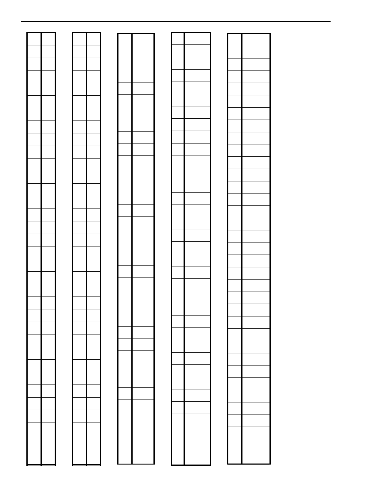
between the input and output ST-BUS stream and
the CEPT line is illustrated in Figures 8 to 12. In
common channel signalling mode timeslot 16
becomes an active channel. In this mode c han nel 16
on DSTi is transmitted on timeslot 16 of the CEPT
link unaltered. This mode is activated by bit 5 of
channel 31 of CSTi0.
Bit Number
1 2 3 45678
Timeslot 0 containing the
frame alignment signal
Timeslot 0 containing the
non-frame alignment signal
Reserved for
International
(1)
use
Reserved for
International
(2)
use
0 0 11011
1 Alarm indication to the
remote PCM multiplex
equipment
Figure 4 - Allocation of Bits in Timeslot 0 of the CEPT Link
Note 1 : With CRC active, this bit is ignored.
Note 2 : With SiMUX active, this bit transmits SMF CRC re sults in frames 13 and 15
Note 3 : Reserved for National use
Timeslot 16 of frame 0 Timeslot 16 of frame 1
ABCD bits for
telephone
channel 16
(timeslot 17)
• • •
0000 XYXX
ABCD bits for
telephone
channel 1
(timeslot 1)
Figure 5 - Allocation of Bits in Timeslot 16 of the CEPT Link
See
Note
#3
ABCD bits for
channel 15
(timeslot 15)
See
Note
#3
See
Note
#3
See
Note
#3
Timeslot 16 of frame 15
ABCD bits for
telephone
telephone
channel 30
(timeslot 31)
See
Note
#3
.
4-165
MT8979 ISO-CMOS
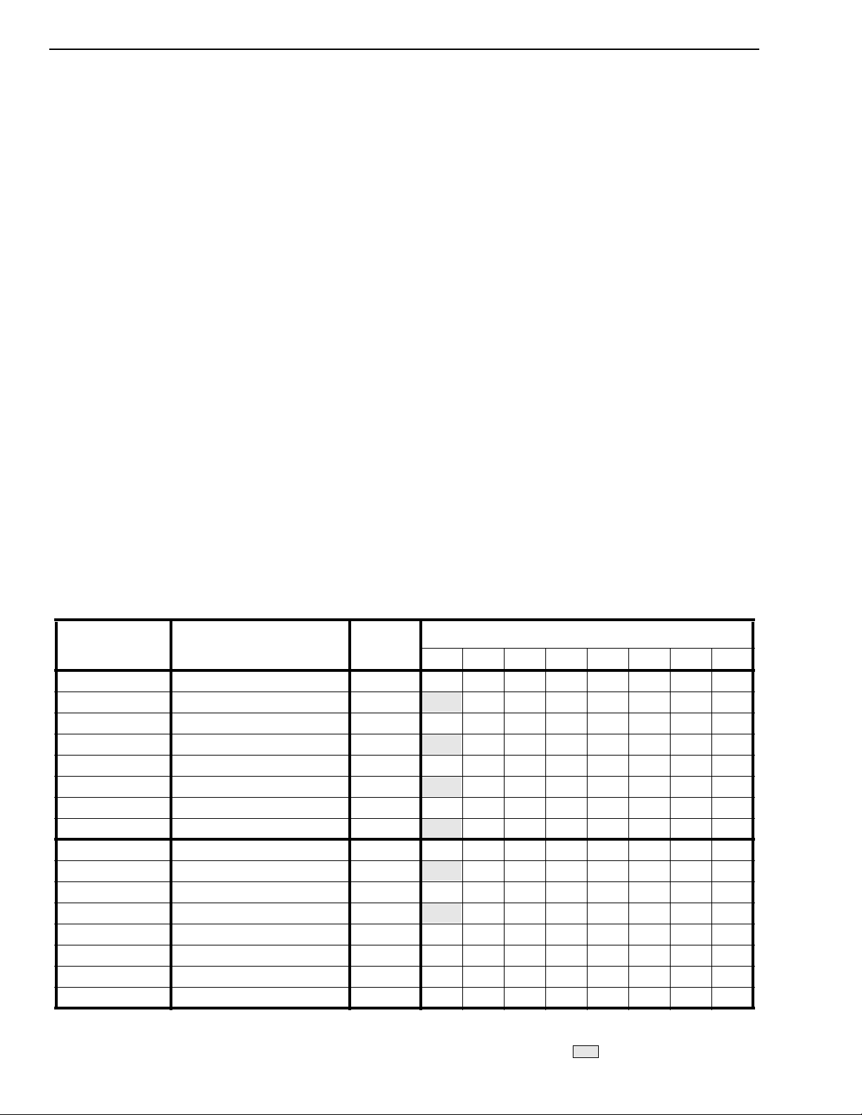
Control Input 0 (CSTi0)
All the necessary control and signalling information
is input through the two control stream s. Control
ST-BUS input number 0 (CSTi0) contains the control
information that is associated with each information
channel. Each control channel contains the per
channel digital attenuation information, the individual
loopback control bit, and the voice or data channel
identifier, see Table 2. When a channel is in data
mode (B7 is high) the digital attenuation and
Alternate Digit Inversion are disabled. It should be
noted that the control word for a given information
channel is input one timeslot early, i.e., channel 0 of
CSTi0 controls channel 1 of DSTi. Channels 15 and
31 of CSTi0 contain Master Control Words 1 and 2,
which are used to set up the interface feature as
seen by the respective bit functions of Tables 3 and
4.
Control In put 1 (CSTi1)
Control ST-BUS input stream number 1 (CSTi1)
contains the synchronization information and the A,
B, C & D signalling bits for insertion into timeslot 16
of the CEPT stre am (refer to Tables 5 to 8 ). Timesl ot
0 contains the four zeros of the multiframe alignment
signal plus the XYXX bits (see Figure 5). Channels 1
to 15 of CSTi1 contain the A, B, C & D signalling bits
as defined by the CEPT format (see Figure 5), i.e.,
channel 1 of CSTi1 contains the A,B,C & D bits for
DSTi timeslots 1 and 17. Channel 16 contains the
frame alignment signal, and channel 17 contains the
non-frame alignment signal (see Figure 4). Channel
18 contains the Master Control Word 3 (see Table 9).
Figure 11 shows the relationship between the control
stream (CSTi1) and the CEPT stream.
Control Output (CSTo)
Control ST-BUS output (CSTo) contains the
multiframe signal from timeslot 16 of frame 0 (see
Table 10). Signalling bits A, B, C & D for each CEPT
channel are sourced from timeslot 16 of frames 1-15
and are output in channels 1-15 on CSTo , as shown
in Table 11. The frame alignment signal and
nonframe alignment signal, received from timeslot 0
of alternate frames, are output in timeslots 16 and 17
as shown in Tables 12 and 13.
Channel 18 contains a Master Status Word, which
provides to the user information needed to determine
the operating condition of the CEPT interface i.e.,
frame synchronization, multiframe synchronization,
frame alignment byte errors, slips, alarms, and the
logic of the external status pin (see Table 14). Figure
12, shows the relationship between the control
stream channels and the CEPT signalling channels
in the multiframe. The ERR bit in the Master Status
word is an indicator of the number of errored frame
alignment bytes that have been received in alternate
timeslot zero. The time interval between toggles of
Multiple Fr am e
Componen t
Frame Type
CRC
Frame #
Frame Alignment Signal 0 C
Non-Frame Alignment Signal 1
S Frame Alignment Signal 2 C
M Non-Frame Alignment Signal 3
F Frame Alignment Signal 4 C
Non-Frame Alignment Signal 5
I Frame Alignment Signal 6 C
Non-Frame Alignment Signal 7
Frame Alignment Signal 8 C
S Non-Frame Alignment Signal 9
M Frame Alignment Signal 10 C
F Non-Frame Alignment Signal 11
Frame Alignment Signal 12 C
I Non-Frame Alignment Signal 13 Si1
I Frame Alignment Signal 14 C
Non-Frame Alignment Signal 15 Si2
Figure 6 - CRC Bit Allocation and Submultiframing
Note 1 : Remote Alarm. Keep at 0 for normal operation.
Note 2 : Reserv ed for Nati onal use. Keep at 1 for norma l opera tion .
Note 3 : Used to monitor far-e nd CRC e rro r perform ance.
Timeslot Zero
12345678
0011011
1
01A
0011011
2
01A
0011011
3
11A
0011011
4
01A
0011011
1
11A
0011011
2
11A
0011011
3
(3)
1A
0011011
4
(3)
1A
(1)
(1)
(1)
(1)
(1)
(1)
(1)
(1)
Sn
Sn
Sn
Sn
Sn
Sn
Sn
Sn
(2)
(2)
Sn
(2)
Sn
(2)
Sn
(2)
Sn
(2)
Sn
(2)
Sn
(2)
Sn
(2)
Sn
multiframe alignment signal
(2)
Sn
(2)
(2)
Sn
(2)
(2)
Sn
(2)
(2)
Sn
(2)
(2)
Sn
(2)
(2)
Sn
(2)
(2)
Sn
(2)
(2)
Sn
indicates position of CRC-4
Sn
Sn
Sn
Sn
Sn
Sn
Sn
Sn
(2)
(2)
(2)
(2)
(2)
(2)
(2)
(2)
Sn
Sn
Sn
Sn
Sn
Sn
Sn
Sn
(2)
(2)
(2)
(2)
(2)
(2)
(2)
(2)
4-166
125µs
ISO-CMOS MT8979
CHANNEL
31
CHANNEL
030
Most
Significant
Bit (First)
BIT
• • •
BIT
7654321
BIT BIT
Figure 7 - ST-BUS Strea m Form at
the ERR bit can be used to evaluate the bit error
rate of the line according to the CCITT
Recommendation G.732 (see section on Frame
Alignment Error Counter).
Channel 19 contains the Phase Status Word (see
Table 15), which can be used to determine the phase
relations hip b e tw ee n the ST-BUS fra me p u l se (F0i
and the rising edge of E8Ko. This information could
be used to determine the long term trend of the
received data rate, or to identify the direction of a
slip.
Channel 20 cont ains the CRC error count (see Table
16). This counter will wrap around once terminal
count is achieved (256 errors). If the maintenance
option is selected (bit 3 of MCW3) the counter is
reset once per se c on d .
Channel 21 contains the Master Status Word 2 (see
Table 17). This byte identifies the status of the CRC
reframe and CRC sync. It also reports the Si bits
received in timeslot 0 of frames 13 and 15 and
the ninth and most significant bit (b8) of the 9-bit
Phase Status Word.
Elastic Buffer
CHANNEL
BIT BIT BIT
(8/2.048 )µ s
CHANNEL
31
CHANNEL
BIT
0
0
Least
Significant
Bit (Last)
selected as the clock source for the PBX) then the
data rate at which the data is being written into the
device on the line side may differ from the rate at
which it is being read out on the ST-BUS side.
When the clocks are not phase-locked, two
situations can occur:
)
Case #1:
If the data on the line side is being written
in at a rate SLOWER than it is being read out on the
ST-BUS side, the distance between the write pointer
and the read pointer will begin to decrease over time.
When the distance is less than two channels, the
buffer will perform a controlled slip which will move
the read pointers to a new location 34 channels
away from the write pointer. This will result in the
REPETITION of the received frame.
Case #2:
If the data on the line side is being written
in at a rate FASTER than it is being read out on the
ST-BUS side, the distance between the write pointer
and the read pointer will begin to increase over time.
When the distance exceeds 42 channels, the elastic
buffer will perform a controlled slip which will move
the read point er to a new location ten channels away
from the write pointer. This will result in the LOSS of
the last r e ce iv e d fra m e .
The MT8979 has a two frame elastic buffer at the
receiver, which absorbs the jitter and wander in the
received signal. The received data is written into the
elastic buffer with the extracted E2i (2048 kHz) clock
and read out of the buff er on the ST-BUS side with
the system C2i (2048 kHz) clock (e.g., PBX system
clock). Under normal operating conditions, in a
synchronous network, the system C2i clock is
phase-locked to the extracted E2i clock. In this
situation every write operation to the elastic buffer is
followed by a read operation. Therefore, underflow
or overflow of data in the elastic buffer will not occur.
If the system clock is not phase-locked to the
extracted clock (e.g., lower qu ality li nk which is not
Note that when the device performs a controlled slip,
the ST-BUS address pointer is repositioned so that
there is either a 10 channel or 34 channel delay
between the input CEPT frame and the output
ST-BUS frame. Since the buffer performs a
controlled slip only if the delay exceeds 42 channels
or is less than two channels, there is a minimum
eight channel hysteresis built into the slip
mechanism. The device can, therefore, absorb eight
channels or 32.5µs of jitter in the received signal.
There is no loss of frame synchronization, multiframe
synchronization or any errors in the signalling bits
when the device performs a slip.
4-167
MT8979 ISO-CMOS
0
17 18 19 20 21 22 23 24 25 26 27 28 29 30 31
CCS
Figure 8 - Relationship between Input DSTi Channels and Transmitted CEPT Timeslots
123456789101112131415
0 1 2 3 4 5 6 7 8 9 10 11 12 13 14 15 16 17 18 19 20 21 22 23 24 25 26 27 28 29 30 31
17 18 19 20 21 22 23 24 25 26 27 28 29 30 31
SIG
Figure 9 - Relationship between Received CEPT Timeslots and Output DSTo Channels
012345678910111213141516171819202122232425262728293031
0 1 2 3 4 5 6 7 8 9 10 11 12 13 14 15 16 17 18 19 20 21 22 23 24 25 26 27 28 29 30 31
0 1 2 3 4 5 6 7 8 9 10 11 12 13 14 15
123456789101112131415 171819202122232425262728293031
Figure 10 - Relationship between Input CSTi0 Channels and Controlled CEPT Timeslots
0 1 2 3 4 5 6 7 8 9 10 11 12 13 14 15 16 17 18 19 20 21 22 23 24 25 26 27 28 29 30 31
N
A
15
14
13
12
11
10
9
8
7
6
5
4
3
2
1
0
0
16
16
16
16
16
16
16
16
16
16
16
16
16
16
16
16
Figur e 11 - Rel atio ns hip b etw ee n In put CSTi 1 Ch a nnel s and Tran smi tte d C EP T Fra m es
0 1 2 3 4 5 6 7 8 9 10 11 12 13 14 15 16 17 18 19 20 21 22 23 24 25 26 27 28 29 30 31
N
A
15
14
13
12
11
10
9
8
7
6
5
4
3
2
1
0
0
0
16
16
16
16
16
16
16
16
16
16
16
16
16
16
16
16
Figure 12- Relationship between Received CEPT Frames and Output CSTo Channels
4-168
DSTi
Channel #
DSTi
CEPT
Timeslot #
Channel #
CEPT
Timeslot #
CSTi0
Channel #
Device Control C1 C2
Control Word
CEPT Ch annel #
CSTi1
Channel #
CEPT
Device Control C3*************
FRAME #
CHANNEL #
CSTo
Channel #
Device Status S1S2S3S4**********
CEPT
FRAME #
TIMESLOT #
- *Denotes U n us ed C h an ne l ( CSTo output is not put in high impeda nc e state) -CCS Denotes Signalling Channel if Common Channel Signalling Mode Selected
- A Deno tes F ram e-Align m en t Fr am e -S1 Denotes Master Status Word 1 (MSW1)
- N Deno tes No n Frame- Al ig nm en t Frame -S2 Denotes Phase Status Word (PSW)
- C1, C2, C3 Denotes Master Control Words 1,2,3 -S3 Denotes CRC Error Count
- SIG Denotes Signalling Channel -S4 Denotes Master Status Word 2 (MSW2)
 Loading...