MITEL MT89760B, MT89760BN, MT89760BS Datasheet
4-55
Features
• Complete in terfac e to a bi direct iona l T1 link
• D3/D4 or ESF frami ng and S LC-96 comp atib le
• Two frame elastic buffer with 32µs j itter buffer
• Insertion and dete ction of A, B, C, D bits
Signalling freeze , opt iona l debo unc e
• Selectable B8ZS, jammed bit (ZCS) or no zero
code suppression
• Yellow and blue al arm signa l ca pabil ities
• Bipolar violation count, F
T
error count, CRC
error count
• Frame and superframe sync. signals, Tx and Rx
• Per channel , overa ll, and re mote l oop aro und
• 8 kHz synchronization output
• Digital phas e det ector betwe en T1 li ne and S TBUS
• ST-BUS compatible
• Pin compatible with the MH89760
• Inductorless clock recovery
• Loss of Sign al (LO S) indi cation
• Available in standard, narrow and surface
mount form ats
Applications
• DS1/ESF digital trunk interfaces
• Computer to PBX interfaces (DMI and CPI)
• High speed comp uter t o com pute r data links
Descript io n
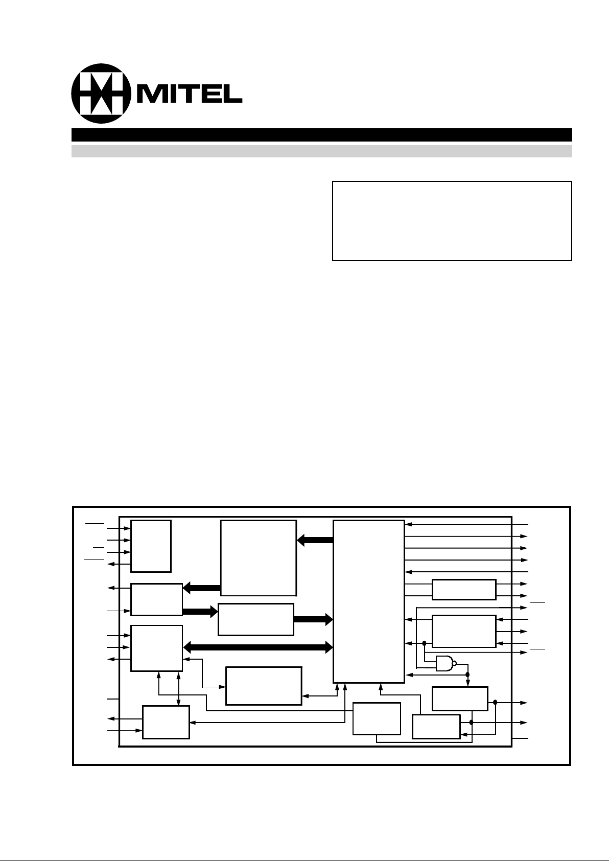
The MH89760B is a complete T1 interface solution,
meeting the Extended Super Frame (ESF), D3/D4
and SLC-96 formats. The MH89760B interfaces to
the DS11.544 Mbit/s ec digital trun k .
The MH89760B is a pin-compatible enhancement of
the MH89760, permitting the removal of the tuneable
inductor and inclusion of the external NAND gate
used for generating RxD.
Figure 1 - Functional Block Diagram
TxSF
C2i
F0i
RxSF
DSTo
DSTi
CSTi0
CSTi1
CSTo
VDD
XCtl
XSt
C1.5i
RxFDLClk
RxFDL
TxFDLClk
TxFDL
OUTA
OUTB
RxA
RxT
LOS
RxR
RxB
E1.5o
E8Ko
VSS
ST-BUS
Timing
Circuitry
Data
Interface
Serial
Control
Interface
Control
Logic
1544-2048
Two Frame
Elastic
Buffer
2048 - 1544
Converte r
ABCD
Signalling RAM
DS1
LINK
INTERFACE
Phase
Detector
DS1
Counter
Clock
Extractor
Receiver
Transmit ter
ISSUE 5 May 1995
Ordering Information
MH89760B 40 Pin DIL Hybrid 1.3" row pitch
MH89760BN 40 Pin DIL Hybrid 0.8" row pitch
MH89760BS 40 Pin Surface Mount Hybrid
0°C to 70°C
MH89760B
T1/ESF Framer & Interface
ST-BUS FAMILY
Preliminary Information
4-56
MH89760B Preliminary Information
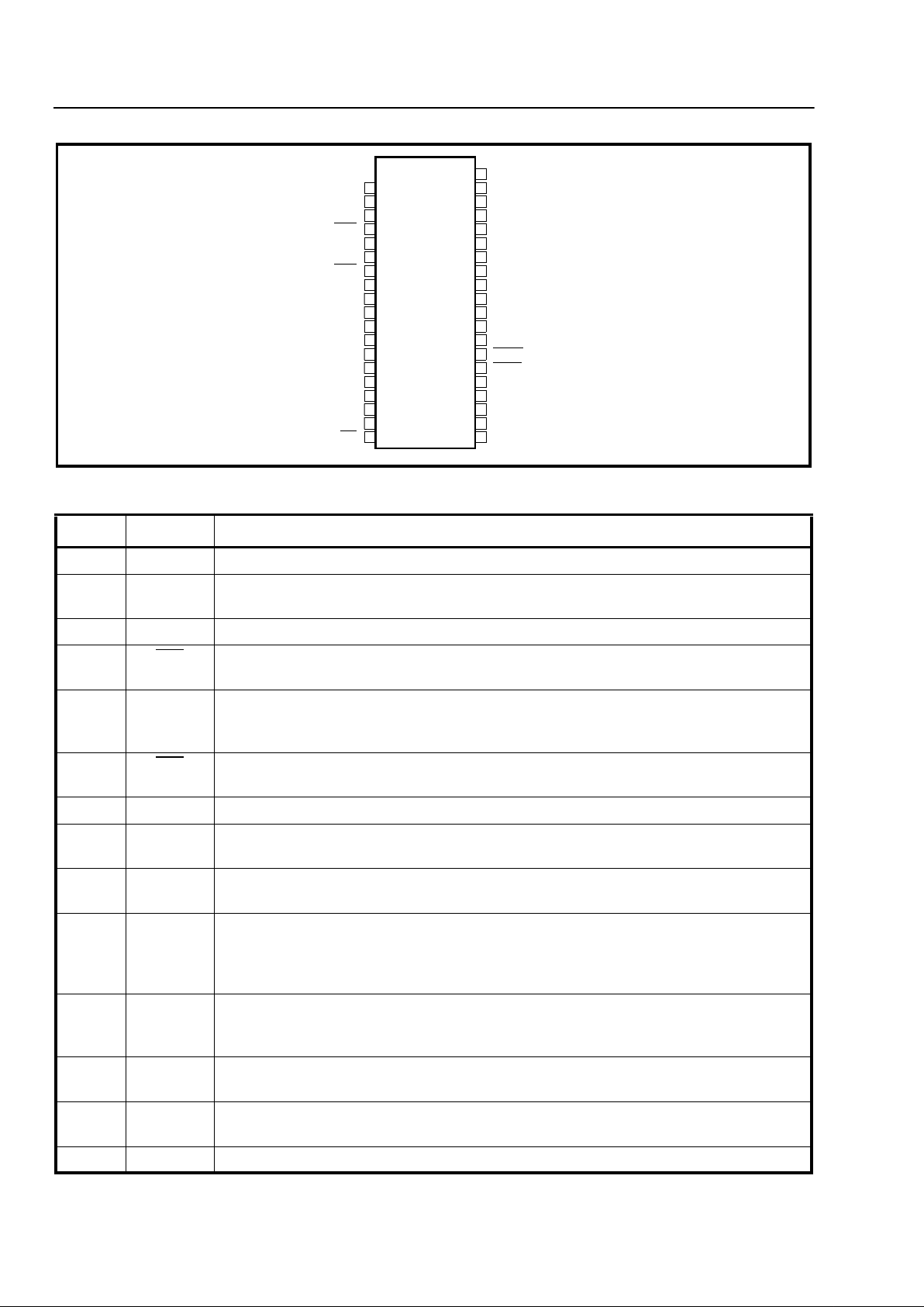
Figure 2 - Pin Connections
Pin Description
Pin # Name Description
2NCNo Connection.
3E1.5o1.544 MHz Extracted Clock (Outpu t): This clock is ext racted by t he device from the
received DS1 signal. It is used internally to clock in data received at RxT and RxR.
4V
DD
System Power S up ply. +5V.
5RxA
Received A (Output): The bipolar DS1 signal received by the device at RxR and RxT is
converted to a unipolar format and output at this pin.
6
7
RxT
RxR
Receive Tip and Ring Inputs: Bipolar split phase inputs designed to be connected
directly to the input transformer. I mpe dance to ground is approximately 1kΩ.
Impedance between pins=430Ω.
8RxB
Received B (Output): The bipolar DS1 signal received by the device at RxR and RxT is
converted to a unipolar format and output at this pin.
9NCNo Connection.
10 CSTi1 Control ST-BUS Input #1: A 2048 kbit/s serial control stream which carries 24 per-
channel control words.
11 CSTi0 Control ST-BUS Input #0: A 2048 kbit/s serial contro l stream that contain s 24 per
channel control words and two master control words.
12 E8Ko 8 kHz Extracted Clock (Outp ut): This is an 8 kH z out put generated by dividing the
extracted 1.544 MHz clock by 193 and aligning it with the received DS1 frame. The 8
kHz signal can be used for synchronizing system clocks to the extracted 1.544 MHz
clock. When digital loopback is enabled, the 8kHz is derived from C1.5.
13 XCtl External Control (Outpu t): This is an uncommitted externa l outpu t pin which is set or
reset via bit 3 in Master Control Word 1 on CSTi0. The state of XCtl is updated once per
frame.
14 XSt External Status (Schmitt Trigger Input): The state of this pin is sampled once per
frame and the status is reported in bit 5 of Master Status Word 2 on CSTo.
15 CSTo Control ST-BUS Output: This is a 2048 kbit/s serial control stream which provides the
24 per-channel status words, and two master status words.
16 NC No Connection.
NC
LOS
NC
TxFDL
NC
TxFDLClk
VSS
RxFDLClk
DSTo
RxFDL
OUTB
C1.5i
RxSF
TxSF
OUTA
NC
NC
NC
VSS
NC
NC
E1.5o
VDD
RxA
RxT
RxR
RxB
NC
CSTi1
CSTi0
E8Ko
XCtl
XSt
CSTo
NC
DSTi
C2i
E1.5o
F0i
2
3
4
5
6
7
8
9
10
11
12
13
14
15
16
17
18
19
20
40
39
38
37
36
35
34
33
32
31
30
29
28
27
26
25
24
23
22
21
4-57
Preliminary Information MH89760B
Pin # Name Description
17 DSTi Data ST-BUS Input: This pin accepts a 2048 kbit/s serial stream which contains the 24
PCM or data channels to be transmitted on the T1 trunk.
18 C2i 2.048 MHz S ystem Clock (Inp ut ): This is the master cl oc k for the ST-BUS section of
the chip. All data on the ST-BUS is clocked in on the falling edge of C2i and out on the
rising edge.
19 E1.5o 1.544 MHz Extracted Clock (Outpu t): Internally connected t o Pin 3.
20 F0i
Frame Pulse Input: This is the frame synchronizati on si gnal which def ines the
beginning of the 32 channel ST-BUS frame.
21 V
SS
System ground .
22-24 NC No Connec tion .
25 OUTA Output A (Open Collector Output): This is the output of the DS1 transmitter circuit. It is
suitable for use with an external pulse transformer to generate the transmit bipolar line
signal.
26 TxSF
Transmit Superframe Pulse Input: A low pulse applied at this pin will det erm ine the
start of the next transmit superframe as illustrated in Figure 20. The device will free run if
this pin is held high.
27 RxSF
Received Superframe Pulse Output: A pulse output on this pin indicates tha t the next
frame of data on the ST-BUS is from frame 1 of the received superframe. The period is
12 frames long in D3/D4 modes and 24 frames in ESF mode. Active only when device is
synchronized to received DS1 signal.
28 C1.5i 1.544 MHz Clock Input: The rising edge of this clock is used to output data on OUTA,
OUTB. C1.5i must be pha se -lo c ked to the C2i system cl o c k.
29 OUTB Output B (Open Collector Output): This is the output of the DS1 transmitter circuit. It is
suitable for use with an external pulse transformer to generate the transmit bipolar line
signal.
30 RxFDL Received Facility Data Link (Output): A 4 kbit/s serial output stream that is
demultiplexe d from the FDL bits in ESF mode, or the received F
S
bit pattern when in
SLC96 mode. It is clocked out on the rising edge of RxFDLClk.
31 DSTo Data ST-BUS Output: A 2048 kbit/s serial output stream which contains the 24 PCM or
data channels received from the DS1 line.
32 RxFDLClk Receive Facility Data Link Cl ock Ou tput: A 4 kHz clock used to output FDL
information on RxFDL. Dat a is clocked out on the rising edge of the clock.
33 V
SS
No Connection.
34 TxFDLCl k Transmit Facility Data Link Clock Outp ut: A 4 kHz clock used to input FDL
information on TxFDL. Data is cloc ked in on the rising edge of the clock.
35 NC No Connection.
36 TxFDL Transmit Facility Data Link (Input)
: A 4 kbit/s serial input stream that is muxed into the
FDL bits in the ESF mode, or the F
S
pattern when in SLC96 mode. It is clocked in on the
rising edge of TxFDLClk.
37 NC No Connection.
38 LO S Loss of Signal (Output): This pin goes high when 128 contiguous ZEROs are received
on the RxT and RxR inputs. When LOS is high, RxA
and RxB are forced high. LOS is
reset when 48 ones are received in a two T1-frame period.
39 NC No Connection.
40 NC No Connection .
Pin Description (Contin ue d)
4-58
MH89760B Preliminary Information
ST-BUS CHANNEL VERSUS DS1 CHANNEL TRANSMITTED
ST-BUS CHANNEL VERSUS DS1 CHA NNEL RECEIVED
PCCW=P er C hannel Con trol Word, M C W1 /2= M as te r C o ntrol Word 1/ 2
ST-BUS CHANNEL VERSUS DS1 CHANNEL CONTROLLED
PCCW=Per Channel Control Word
ST-BUS CHANNEL VERSUS DS1 CHANNEL CONTROLLED
PCSW=Per Channel Status Word, PSW=Phase Status Word, MSW=Master Status Word
ST-BUS VERSUS DS 1 CHANNEL STATUS
X = UNUSED
Figure 3 - ST-BUS Channel Allocations
DSTi 0
X
1234
X
5678
X
9 101112
X
13 14 15 16
X
17 18 19 20
X
21 22 23 24
X
25 26 27 28
X
29 30 31
DS1 1 2 3 4 5 6 7 8 9 10 11 12 13 14 15 16 17 18 19 20 21 22 23 24
DSTo 0
X
1234
X
5678
X
9101112
X
13 14 15 16
X
17 18 19 20
X
21 22 23 24
X
25 26 27 28
X
29 30 31
DS1 1 2 3 4 5 6 7 8 9 10 11 12 13 14 15 16 17 18 19 20 21 22 23 24
CSTi0 0
PC
CW
1
1
PC
CW
1
2
PC
CW
1
3
X
4
PC
CW
1
5
PC
CW
1
6
PC
CW
1
7
X
8
PC
CW
1
9
PC
CW
1
10
PC
CW
1
11
X
12
PC
CW
1
13
PC
CW
1
14
PC
CW
1
15
MC
W1
16
PC
CW
1
17
PC
CW
1
18
PC
CW
1
19
X
20
PC
CW
1
21
PC
CW
1
22
PC
CW
1
23
X
24
PC
CW
1
25
PC
CW
1
26
PC
CW
1
27
X
28
PC
CW
1
29
PC
CW
1
30
PC
CW
1
31
MC
W2
DS1 1 2 3 4 5 6 7 8 9 10 11 12 13 14 15 16 17 18 19 20 21 22 23 24
CSTi1
0
PC
CW
2
1
PC
CW
2
2
PC
CW
2
3
X
4
PC
CW
2
5
PC
CW
2
6
PC
CW
2
7
X
8
PC
CW
2
9
PC
CW
2
10
PC
CW
2
11
X
12
PC
CW
2
13
PC
CW
2
14
PC
CW
2
15
X
16
PC
CW
2
17
PC
CW
2
18
PC
CW
2
19
X
20
PC
CW
2
21
PC
CW
2
22
PC
CW
2
23
X
24
PC
CW
2
25
PC
CW
2
26
PC
CW
2
27
X
28
PC
CW
2
29
PC
CW
2
30
PC
CW
2
31
X
DS1 1 2 3 4 5 6 7 8 9 10 11 12 13 14 15 16 17 18 19 20 21 22 23 24
CSTo 0
PCS
W
1
PCS
W
2
PCS
W
3PSW
4
PCS
W
5
PCS
W
6
PCS
W
7
X
8
PCS
W
9
PCS
W
10
PCS
W
11
X
12
PCS
W
13
PCS
W
14
PCS
W
15
MS
W1
16
PCS
W
17
PCS
W
18
PCS
W
19
X
20
PCS
W
21
PCS
W
22
PCS
W
23
X
24
PCS
W
25
PCS
W
26
PCS
W
27
X
28
PCS
W
29
PCS
W
30
PCS
W
31
MS
W2
DS1 1 2 3 4 5 6 7 8 9 10 11 12 13 14 15 16 17 18 19 20 21 22 23 24

4-59
Preliminary Information MH89760B
Functional Description
The MH89760B is a thick film hybrid solution for a T1
interface. All of the formatting and signalling
insertion and detection is done by the device.
Various programmable options in the device include:
ESF, D3/D4 or SLC-96 mode, common channel or
robbed bit signalling, zero code suppression, alarms,
and local and remote loopback. The MH89760B also
has built in bipolar line drivers and receivers and a
clock extraction circuit.
All data and control information is communicated to
the MH89760B via 2048 kbit/s serial streams
conforming to Mitel’s ST-BUS format.
The ST-BUS is a TDM serial bus that operates at
2048 kbits/s. The serial streams are divided into 125
µsec frames that are made up of 32 8-bit channels. A
serial stream that is made up of these 32 8 bit
channels is known as an ST-BUS stream, and one of
these 64 kbit/s channels is known as an ST-BUS
channel.
The system side of the MH89760B is made up of STBUS inputs and outputs, i.e., control inputs and
outputs (CSTi/o) and data inputs and outputs
(DSTi/ o). These signals are functionally represented
in Figure 32. The DS1 line side of the device is made
up of split phase inputs (RxT, RxR) and outputs
(OUTA, OUTB) which can be connected to line
coupling transformers. Functional transmit and
receive timing is shown in Figures 33 and 34.
Data for transmission on the DS1 line is clocked
serially into the device at the DSTi pin. The DSTi pin
accepts a 32 channel time division multiplexed STBUS stream . Data i s clocked in wit h the falli ng edge
of the C2i clock. ST-BUS frame boundaries are
defined by the frame pulse applied at the F0i pin.
Only 24 of the available 32 c hannels on the ST-BUS
serial stream are actually transmitted on the DS1
side. The unused 8 channels are ignored by the
device.
Data recei ved fr om the DS1 l ine i s cl o c ke d o ut of th e
device in a similar manner at the DSTo pin. Data is
clocked out on the rising edge of the C2i clock. Only
24 of the 32 channels output by the device contain
the information from the DS1 line. The DSTo pin is,
however, actively driven during the unused channel
timeslots. Figure 3 shows the correspondence
between the DS1 channels and the ST-BUS
channels.
All control and monitoring of the device is
accomplished through two ST-BUS serial control
inputs and one ser ial control outpu t. Control ST-BUS
input number 0 (CSTi0) accepts an ST-BUS serial
stream which contains the 24 per channel control
words and two master control words. The per chan nel
control words relate directly to the 24 information
channels output on the DS 1 side. The master control
words affect operation of the whole device. Control
ST-BUS input number 1 (CSTi1) accepts an ST-BUS
stream containing the A, B, C and D signalling bits.
The relationship between the CSTi channels and the
controlled DS0 channels is shown in Figure 3. Status
and signalling inform ation is received from the device
via the control ST-BUS output (CSTo). This serial
outpu t stream contain s two m aster st atus wo rds, 24
per channel status words and one Phase Status
Word. Figure 3 shows the correspondence between
the received DS1 channels and the status words.
Detailed information on the operation of the control
interface is presented be low.
Program mabl e Feat ures
The main features in the device are programmed
through two master control words which occupy
channels 15 and 31 in Control ST-BUS input stream
number 0 (CSTi0). These two eight bit words are
used to:
• Select the di fferent op erati ng mo de s of the
device ESF, D3/D4 or SLC-96.
• Activate th e fea tures th at are n ee ded in a
certain application; common channel signalling,
zero code supp ressi on, signal ling d eboun ce,
etc.
• Turn on in service alarm s, d iagno stic lo op
arounds, and the ext erna l cont rol funct ion.
Tables 1 and 2 contain a complete explanation of the
function of the different bits in Master Control Words
1 and 2.
Major Operating Modes
The major operating modes of the device are
enabled by bits 2 and 4 of Master Control Word 2.
The Extended Superframe (ESF) mode is enabled
when bit 4 is set high. Bit 2 has no effect in this
mode. The ESF mode enables the t ransmission of
the S bit pattern shown in Table 3. This includes the
frame/superframe pattern, the CRC-6, and the
Facility Data Link (FDL). The device generates the
frame/multiframe pattern and calculates the CRC for
each superframe. The data clocked into the device
on the TxFDL pin is incorporated into the FDL. ESF
mode will also insert A, B, C and D si gnalling bits into
the 24 f rame multiframe. The DS1 frame begins after
approximately 25 periods of the C1.5i clock from the
F0i
frame pulse.

4-60
MH89760B Preliminary Information
.
Table 1. Master Control Word 1 (Channel 15, CSTi0)
Table 2. Master Control Word 2 (Channel 31, CSTi0)
Bit Name Description
7 Debounce When set the received A, B, C and D signalling bits are reported directly in the per
channel status words output at CSTo. When clear, the signalling bits are debounced for
6 to 9 ms before they are placed on CSTo.
6 TSPZCS Transparent Zero Code Suppression. When this bit is set, no zero code suppression is
implemented.
5 B8Z S Bin ary Eig ht Zero Supp ressi on . When this bit is set, B8ZS zero code suppression is
enabled. When clear, bit 7 in data channels containing all zeros is forced high before
being transmitted on the DS1 side. This bit is inactive if the TSPZCS bit is set.
4 8kHSel 8 kHz Output Select. Whe n set, the E8K o pin is held high. Whe n clear, the E8Ko
generates an 8 kHz output derived from the extracted 1.544 MHz clock or C1.5i clock
(see Pin Description for E8Ko).
3 XC tl External Control Pin. When set, the XCtl pin is held high. Whe n clea r, XCtl is held low.
2 ESFYLW ESF Yellow Alarm. Valid only in ESF mode. When set, a sequence of eight 1’s followed
by eight 0’s is sent in the FDL bit positions. When clear , the FDL bit contains data input at
the TxFDL pin.
1 Robbed bit When this bit is set, robbed bit signalling is disabled on all DS0 transmit channels. When
clear, A, B, C and D signalling bits are inserted into bit position 8 of all DS0 channels in
every 6th frame.
0 YLALR Yellow Alarm. When set, bit 2 of all DS0 channels is set low. When clear, bit 2 operates
normally.
Bit Name Description
7 RMLOOP Remote Loopback. When set, the data received at RxR and RxT is looped back to OUTB
and OUTA respective ly. The data is clocked into t he device wit h the extracted 1.54 4 MHz
clock. The device still monitors the received dat a and outpu ts it at DSTo. The device
operates normally when the bit is clear.
6 DGLOOP Digital Loopback. When set, the data input on DSTi is looped around to DSTo. The
normal received data on RxR and RxT is ignored. However, t he dat a input at DSTi is still
transmitted on OUTA and OUTB. The device frames up on the looped data using the C1.5i
clock.
5 ALL1'S All One’s Alarm. When set, the chip transmits an unfram ed all 1's signal on OUTA and
OUTB.
4 ESF/D4 ESF/D4 Select. W hen set, the device is in ESF mode. When clear, the device is in D3/D4
mode.
3 ReFR Reframe. If set for at least one frame and then cleared, the chip will begi n to search for a
new frame position. Only the change from high to low will cause a reframe, not a
continuous low level.
2 SLC-96 SLC-96 Mode Select. The chip is in SLC-96 mode when this bit is set. This enables input
and output of the F
S
bit pattern using the same pins as the facility data link in ESF mode.
The chip will use the same framing algorithm as D3/D4 mo de. Th e user must insert the
valid F
S
bits in 2 out of 6 superframes to allow the receiver to find superframe sync, and
the transmitter to insert A and B bits in every 6th frame. The SLC-96 FDL completely
replaces the F
S
pattern in the outgoing S bit po sition. I nacti ve in ESF mod e.
1 CRC/MIMIC In ESF mode, when set, the chip disregards the CRC calculation durin g synchroniza tion .
When clear, the device will check for a correct CRC before going into synchronization. In
D3/D4 mode, when set, the device will synchronize on the first correct S-bit pattern
detected. When this bit is clear, the device will not synchronize if it has detected more than
one candidate for the fram e ali gnm ent pat te rn (i.e. , a mimic ).
0 Maint. Maintena nce M ode. When set, the device will declare itself out-of-sync if 4 out of 12
consecutive F
T
bits are in error. When clear, th e out-of -s ync thresh old is 2 errors in 4 FT
bits. In this mode, four consecutive bit s follo wing an errored F
T
bit are examined.

4-61
Preliminary Information MH89760B
Table 3. ESF Fra me Pat ter n
† These signalling bits are only valid if the robbed bit signalli ng is
active.
During synchronization the receiver locks on to the
incoming frame, calculates the CRC and compares it
to the CRC received in the next multiframe. The
device will not declare itself to be in synchronization unless a valid framing pattern in the S-bit is
detected and a correct CRC is received. The CRC
check in this case provides protect ion against false
framing. The CRC check can be turned off by setting
bit 1 in Master Control Word 2.
The device can be forced to resynchronize itself. If
Bit 3 in Master Cont rol Word 2 is set for one frame
and then subsequently reset, the de vice will start to
search for a new frame position. The decision to
reframe is made by the user’s system processor on
the basis of the status conditions detected in the
received master status words. This may include
consideration of the number of errors in the received
CRC in conjunction with an indication of the
presence of a mimic. When the device attains
synchronization the mimic bit in Master Status Word
1 is set if the device found another possible
candidate when it was searching for the framing
pattern.
Note that the devi ce will r esync hroniz e auto matic ally
if the errors in the terminal framing pattern (F
T
or
FPS) exceed the threshold set with bit 0 in Master
Control Word 2.
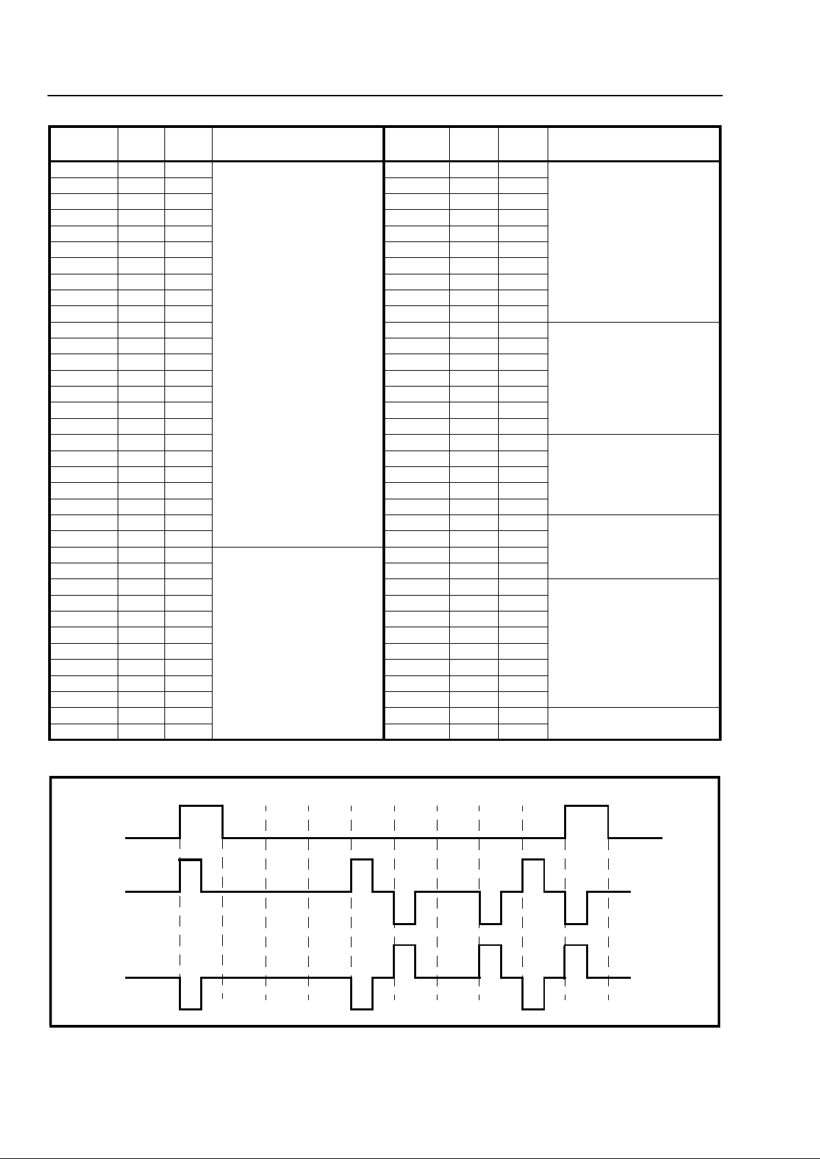
Frame # F PS F DL CRC Signalling
†
1X
2CB1
3X
40
5X
6 CB2 A
7X
80
9X
10 CB3
11 X
12 1 B
13 X
14 CB4
15 X
16 0
17 X
18 CB5 C
19 X
20 1
21 X
22 CB6
23 X
24 1 D
Table 4. D3/D4 Framer
† These signalling bits are only valid if the robbed bit signalling is
active.
Standard D3/D4 framing is enabled when bit 4 of
Master Control Word 2 is reset (logic 0). In this mode
the device searches for and inserts the framing
pattern shown in Table 4. This mode only supports
AB bit signalling, and does not contain a CRC check.
The CRC/MIMIC bit in Master Control Word 2, when
set high, allows the device to synchronize in the
presence of a mimic. If this bit is reset, the device will
not synchronize in the presence of a mimic. (Also
refer t o section on Framing Algorit hm.)
In the D3/D4 mode the device can also be made
compatible with SLC-96 by setting bit two of Master
Control Word 2. This allows the user to insert and
extract the signalling framing pattern on the DS1 bit
stream using the FDL input and output pins. The
user must format this 4 kbits of information exter nally
to meet all of the requirements of the SLC-96
specification (see Table 5). The device multiplexes
and demultiplexes this information into the proper
position. This mode of operation can also be used for
any other application that uses all or part of the
signalling framing pattern. As long as the serial
stream clocked into the TxFDL contains two proper
sets of consecutive synchronization bits (as shown in
Table 5 for fr am es 1 to 2 4) , the devic e will be
able to insert and extract the A, B signalling bits.
The TxSF
pin should be held high in this mode.
Superframe boundaries cannot be defined by a pulse
on this inpu t. The RxSF
output functions normally
and indicates the superframe boundaries based on
the synchronization pattern in the F
S
received bit
position.
Zero Code Suppression
The combination of bits 5 and 6 in Master Control
Word 1 allow one of three zero code suppression
schemes to be selected. The three choices are:
none, binary 8 zero suppression (B8ZS), or jammed
bit (bit 7 forced high). No zero code suppression
Frame # F
T
F
S
Signalling
†
11
20
30
40
51
61A
70
81
91
10 1
11 0
12 0 B
4-62
MH89760B Preliminary Information
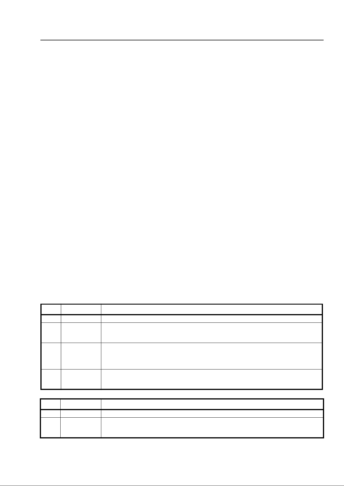
Table 5. SLC-9 6 Fram ing P attern
† Note: The FS pattern has to be supplied by the user.
Figure 4 - B8ZS Output Coding
Frame
#
F
T
F
S
†
Notes
Frame
#
F
T
F
S
†
Notes
11
Resynchronization
Data
Bits
37 1
X = Concentrator
Field Bits
20 38X
30 390
40 40X
51 411
60 42X
70 430
81 44X
91 451
10 1 46 X
11 0 47 0
S = Spoiler Bits
12 1 48 S
13 1 49 1
14 0 50 S
15 0 51 0
16 0 52 S
17 1 53 1
18 0 54 C
C = Maintenance
Field
Bits
19 0 55 0
20 1 56 C
21 1 57 1
22 1 58 C
23 0 59 0
A = Alarm Field
Bits
24 1 60 A
25 1
X =Concentrator
Fiel d Bi ts
61 1
26 X 6 2 A
27 0 63 0
L = Line Sw i tc h
Field Bits
28 X 6 4 L
29 1 65 1
30 X 6 6 L
31 0 67 0
32 X 6 8 L
33 1 69 1
34 X 7 0 L
35 0 71 0
S = Spoiler Bits
36 X 72 S
DATA
B8ZS
B8ZS
B0 00V
B
0
V
B
B
000
V
B
0
V
B
B
V = Violation
B = Bipolar
0 = No Pulse
B
4-63
Preliminary Information MH89760B
allows the device to interface with systems that have
already applied some form of zero code suppression
to the data input on DSTi. B8ZS zero code
suppression replaces all strings of 8 zeros with a
known bit pattern and a specific pattern of bipolar
violations. This bit pattern and violation pattern is
shown in Figure 4. The receiver monitors the
received bit pattern and the bipolar violation pattern
and replaces all matching strings with 8 zeros .
Loopback Modes
Remote and digital loopback modes are enabled by
bits 6 and 7 in Master Cont rol Word 2. These modes
can be used for diagnostics in locating the source of
a fault condition. Remote loop around loops back
data received at RxR and RxT back out on OUTA
and OUTB, thus effectively sending the received
DS1 data back to the far end unaltered so that the
transmission line can be tested. The received signal
with the appropriate received channels on the DS1
side made available in the proper format at DSTo.
The digital loop around mode diverts the data
received at DSTi back out the DSTo pin. Data
received on DSTi is, however, still t ransmitted out via
OUTA and OUTB. This loop back mode can be used
to test the near end interface equipment when there
is no transmission line or when there is a suspected
failure of the line.
The all ones transmit alarm (also known as the blue
alarm or the keep alive signal) can be activated in
conjunction with the digital loop around so that the
transmission line sends an all 1's signal while the
normal data is looped back locally.
The MH89760B also has a per channel loopback
mode. See Table 6 and the following section for more
information.
Per Channel Control Features
In addition to the two master control words in CSTi0
there are also 24 Per Channel Control Words. These
control words only affect individual DS0 channels.
The correspondence between the channels on
CSTi0 and the affected DS0 channel is s hown in Fig.
3. Each control word has three bits that enable
robbed bit signalling, DS0 channel loopback and
inversion of the DS0 channel. A full description of
each of the bits is provided in Table 6.
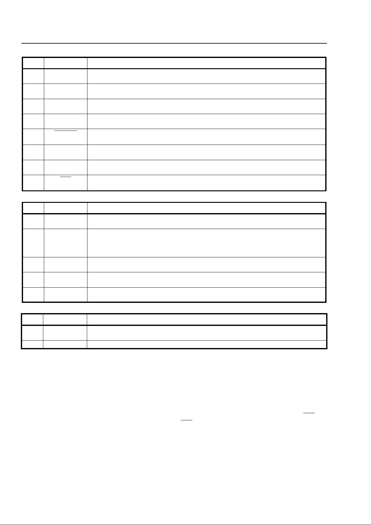
Transmit Signalling Bits
Control ST-BUS input number 1 (CSTi1) contains 24
additional per channel control words. These 24 STBUS channels c ont ain the A, B, C and D signalling
bits that the device uses at transmit time. The
position of these 24 per channel control words in the
ST-BUS is
shown in Figure 3 and the position of the
ABCD signalling bits is shown in Table 7. Even
though the device only inserts the signalling
information in every 6th DS1 frame this information
must be input every ST-B US frame.
Robbed bit signalling can be disabled for all
channels on the DS1 link by bit 1 of M aster Control
Word 1. It can also be disabled on a per channel
basis by bit 0 in the Per Channel Control Word 1.
Table 6. Per Channel Control Word 1 Input at CSTi0
Table 7. Per Channel Control Word 2 Input at CSTi1
Bit Name Description
7-3 IC Internal Connections. Must be kept at 0 for normal operation.
2 Polarity When set, the applicable channel is not inverted on the transmit or the receive side of the device.
When clear, all the bits within the applicable channel are inverted both on transmit and receive
side.
1 Loop Per Channel Loopback. When set, the received DS0 channel is replaced with the transmitted
DS0 channel. Only one DS0 channel may be looped back in this manner at a time. The
transmitted DS0 channel remains unaffect ed. When clear the transmit and receive DS0 sections
operate normally.
0 Data Data Channel Enable. When set, robbed bit si gnalling for the applicable channel is disabled.
When clear, every 6th DS1 frame is available for robbed bi t signalling. This feature is enabled
only if bit 1 in Master Control Word is low.
Bit Name Description
7-4 Unused Keep at 0 for normal operation
3
2
1-0
A
B
C, D
These are the 4 signalling bits inserted in the appropriate channels of the DS1 stream bei ng
output from the chip, when in ESF mode. In D3/D4 modes where there are only two signalling
bits, the values of C and D are ignored.
4-64
MH89760B Preliminary Information
.
Table 8. Master Statu s Word 1 (Chan nel 15 , CSTo)
Table 9. Master Statu s Word 2 (Chan nel 31 , CSTo)
Table 10. Phase Status Word (Channel 3, CSTo)
Bit Name Description
7 YLALR Yellow Alarm Indication. This bit is set when the chip is receiving a 0 in bit position 2 of every
DS0 channel.
6MIMICThis bit is set if the frame search algorithm found more than one possible frame candidate when
it went into frame synchronization.
5 ERR Terminal Framing Bit Error. The state of this bit changes every time the chip detects 4 errors in
the F
T
or FPS bit pattern. The bit will not change state more than once every 96ms.
4 ESFYLW ESF Yellow Alarm. This bit is set when the devi ce has observed a sequence of eight one’s and
eight 0’s in the FDL bit positions.
3 MFSYNC
Multiframe Synchronization. This bit is cleared when D3/D4 multiframe synchronization has
been achieved. Applicable only in D3/D4 and SLC-96 modes of operation.
2 BPV Bipolar Violation Count. The state of this bit changes every time the device counts 256 bipolar
violations.
1 SLIP Slip Indication. This bit changes state every time the elastic buffer in the device performs a
controlled slip.
0SYN
Synchronization. This bit is set when t he device has not achieved synchronization. The bit is
clear when the device has synchronized to the received DS1 data stream.
Bit Na me Description
7 BlAlm Blue Alarm. This bit is set if the receiver has detected two frames of 1’s and an out of frame
condition. It is reset by any 250 microsecond interval that contains a zero.
6 FrCnt Frame Count. This is the ninth and most significant bit of the “Phase Status Word" (see Table
10). If the phase status word is incrementing, this bit will toggle when the phase reading exceeds
channel 31, bit 7. If the phase word is decrementing, then this bit will toggle when the reading
goes below channel 0, bit 0.
5 XSt External Status. T his bit reflects the state of the external status pin (XSt). The state of the XSt
pin is sampled once per frame.
4-3 BP VCnt Bipolar Violation Count. These two bits change state every 128 and every 64 bipolar vio lations,
respectively .
2-0 CRCCNT CRC Error Count. These three bits count recei ved CRC errors. The counter will reset to zero
when it reaches terminal count. Valid only in ESF mode.
Bit Name Description
7-3 ChannelCnt Channel Count. These five bits indicate the ST-BUS channel count between the ST-BUS frame
pulse and the rising edge of E8Ko.
2-0 BitCnt Bit Count. These three bits provide one bit resolution within the channel count described above.
Operating Status Information
Status Information regarding the operation of the
device is output serially via the Control ST-BUS
output (CSTo). The CSTo serial stream contains
Master Stat us Words 1 and 2, 24 Per Channe l Status
Words, and a Phase Status Word. The Mas ter Status
Words contain all of the information needed to
determ i n e th e st ate o f t he int e rf ace a nd ho w w e ll i t i s
operating. The information provided includes frame
and super frame synchronization, slip, bipolar
violation counter, alarms, CRC error count, F
T
error
count, synchronization pattern mimic and a phase
status word. Tables 8 and 9 give a description of each
of the bits in M ast er Statu s Word s 1 and 2, and Table
10 gives a descripti on of the Pha se Sta tus Word .
In addition, the MH89760B has a Loss of Signal
(LOS) pin that is set High when 128 consecutive
ZEROs are recei ved . Wh ile LOS is set High , RxA
and
RxB
are forced High. The LOS signa l goes Low w he n
a ONEs density on 12.5% of the bits (equivalent to 48
bits) occurs in a two DS1 frame period.

4-65
Preliminary Information MH89760B
.
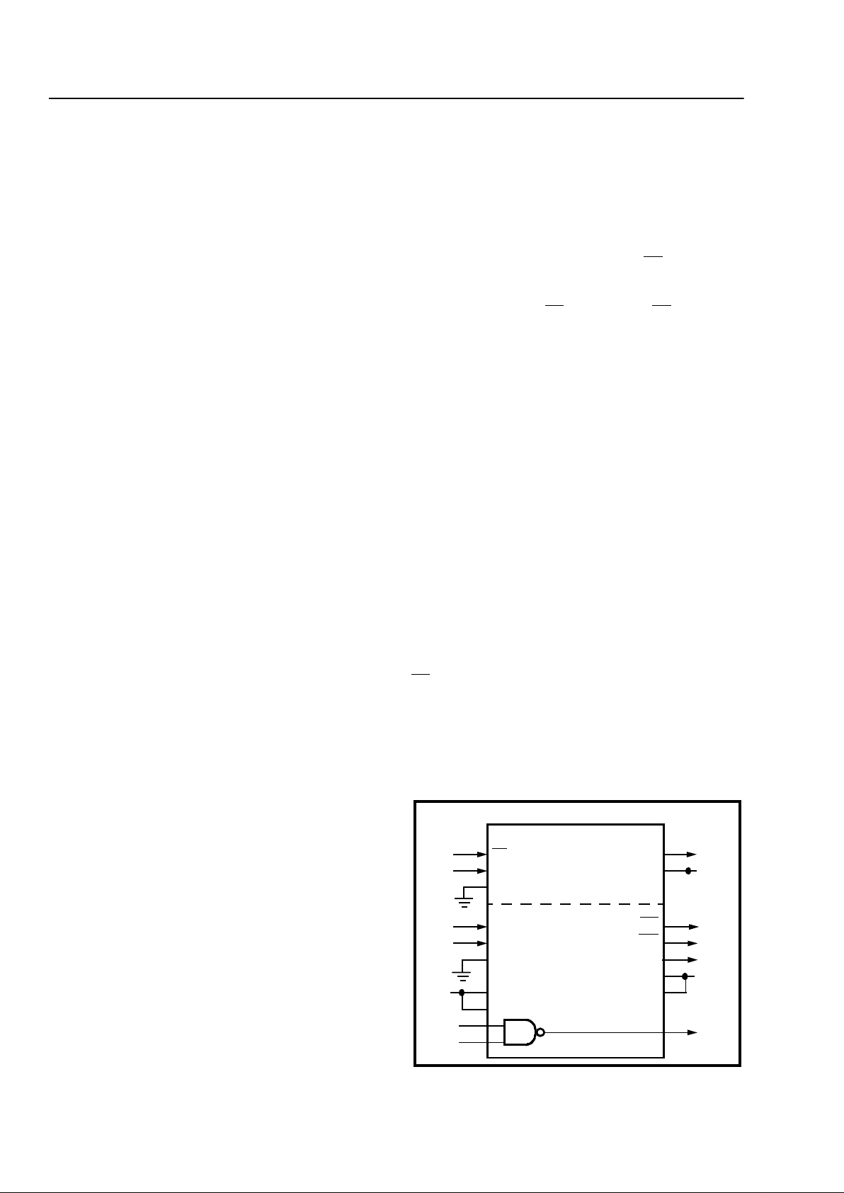
Table 11. Per Channel Status Word Output on CSTo
Bit Name Description
7-4 Unused Unused Bits. Will be output as 0’s.
3
2
1
0
A
B
C
D
These are the 4 signalling bits as extracted from the received DS1 bit stream.
The bits are debounced for 6 to 9 ms if the debounce feature is enabled via bit 7 in Master
Control Word 1.
Alarm Detect ion
The device detects the yellow alarm for both D3/D4
frame format and ESF format. The D3/D4 yellow
alarm will be activated if a ‘0‘ is received in bit
position 2 of every DS0 channel for 600 msec. It will
be released in 200 msec after the content s of the bit
change. The alarm is detectable in the presence of
errors on the line. The ESF yellow alarm will
become active when the device has detected a string
of eight 0’s followed by eight 1’s in the facility data
link. It is not detectable in the presence of errors on
the line. This means that the ESF yellow alarm will
drop out for relatively short periods of time, so the
system will have to integrate the ESF yellow alarm.
The blue alarm signal, in Master Status Word 2, will
also drop out if there are errors on the line.
Mimic Detect ion
The mimic bit in Ma ster Status Word 1 w ill be set if,
during synchronization, a frame alignment pattern
(F
T
or FPS bit pattern) was observed in more than
one position, i.e., if more than one candidate for the
frame synchronization position was observed. It will
be reset w he n t he de vice resynchronizes. T h e mi mi c
bit, the terminal framing error bit and the CRC error
counter can be used separately or together to decide
if the rec eiv e r s ho u ld b e fo r ced to r e fra me.
Bipolar Violation Counter
The Bipolar Violation bit in Master Status Word 1 will
toggle after 256 violations have been detected in the
received signal. It has a maximum refresh t ime of 96
ms. This means that the bit can not change state
faster than once every 96 ms. For example, if there
are 256 violations in 80 ms the BPV bit will not
change state until 96 ms. Any more errors in that
extra 16 ms are not counted. If there are 256 errors
in 200 ms then the BPV bit will change state after
200 ms. In practical terms this puts an upper limit
on the error rate that can be calculated from the BPV
information, but this rate (1.7 X 10
-3
) is well above
any normal operating condition.
Bits 4 and 3 also provide bipolar violations information. Bit 4 will change state after 128 violations.
Bit 3 changes state after 64 bipolar violations. These
bits are refreshed independently and are not subject
to the 96 ms refresh rate described above.
DS1/ST-BUS Phase Difference
An indication of the phase difference between the
ST-BUS and the DS1 frame can be ascertained from
the information provided by the eight bit Phase
Status Word and the F rame Count bit. Channel t hree
on CSTo contains the Phase Status Word. Bits 7-3 in
this word indicate the number of ST-BUS channels
between the ST-BUS frame pulse and the rising
edge of the E8Ko signal. The remaining three bits
provide one bit resolution within the channel count
indicated by bits 7-3. The frame count bit in Master
Status Word 2 is the ninth and most significant bit of
the phase status word. It will toggle when the phase
status word increments above channel 31, bit 7 or
decrements below channel 0, bit 0. The E8Ko signal
has a specific relationship with received DS1 frame.
The rising edge of E8Ko occurs during bit 2, channel
17 of the received DS1 frame. The Phase Status
Word in conjunction with the frame count bit, can be
used to monitor the phase relationship bet ween the
received DS1 frame and the local ST-BUS frame.
The local 2.048 MHz ST-BUS c lock must be phaselocked to the 1.544 MHz clock extracted from the
received data. When the two clocks are not phaselocked, the input data rate on the DS1 side will differ
from the output data rate on the ST-BUS side. If the
average input data rate is higher than the average
output dat a rate, the channel c ount and bit count in
the phase s tatus word will be seen t o decrease over
time, indicating that the E8Ko rising edge, and
therefore the DS1 frame boundary is moving with
respect to the ST-BUS frame pulse. Conversely, a
lower average input data rate will result in an
increase in the phas e reading.
In an application where it is necessary to minimize
jitter transfer from the received clock to the local
system clock, a phase lock loop with a relatively
large time constant can be implemented using
information provided by the phase status word. In
such a system, the local 2.048 MHz clock is derived
from a precision VCO. Frequency corrections are
made on the basis of the average trend observed in
4-66
MH89760B Preliminary Information
the phase status word. For example, if the channel
count in the phase status word is seen to increase
over time, the feedback applied to the VCO is used
to decrease the system clock frequency until a
reversal in the trend is observed.
The elastic buffer in the MH89760B permits the
device to handle eight channels of jitter/wander (see
description of elastic buffer in the next section). In
order to prevent slips from occurring, the frequency
corrections would have to be implemented such that
the deviation in the phase status word is limited to
eight channels peak to peak. It is possible to use a
more sophisticated protocol which would center the
elastic buffer and permit more jitter/wander to be
handled. However, for most applications, the eight
channels of jitter/wander tolerance is acceptable.
Received Signalling Bits
The A, B, C and D signalling bits are output from the
device in the 24 Per Channel Status Words. Their
location in the serial steam output at CSTo is shown
in Figure 3 and the bit positions are shown in Table
11. The internal debouncing of the signalling bits
can be turned on or off by Mast er Control Word 1. In
ESF mode, A, B, C and D bits are valid. Even
though the signalling bits are only received once
every six frames the device stores the information so
that it is available on the ST-BUS every frame. The
ST-BUS will always contain the most recent
signalling bits. The state of the signalling bits is
frozen if synchronization is lost.
In D3/D4 mode, only the A and B bits are valid. The
state of the signalling bits is frozen when terminal
frame synchronization is lost. The freeze is disabled
when the device regains terminal frame
synchronization. The signalling bits may go through
a random transition stage until the device attains
multifram e synchro nization .
Clock and Framing Signals
The MH89760B has a built in clock extraction circuit
which creates a 1.544 MHz clock synchronized to
the received DS1 signal. This clock is used
internally by the MH89760B to clock in data
received on RxT and RxR, and is also output at the
E1.5o pin. The circuit has been designed to
operate within the constraints imposed by the
minimum 1’s density requirements, typically
specified for T1 networks (maximum of 15
consecutive 0’s).
The extracted clock is internally divided by 193 and
aligned with the received D S1 frame. The resulti ng 8
kHz signal is output at the E8Ko pin and can be used
to phase lock the local system C2 and t he transmit
C1.5 clo c ks to the extracted clock .
The MH89760B requires three clock signals which
have to be generated externally. The ST-BUS
interface on the device requires a 2.048 MHz signal
which is applied at the C2i pin and an 8
kHz framing signal applied at the F0i
pin. The
framing signal is used to delimit individual STBUS frames. Figure 19 illustrates the relationship
between the C2i and F0i
signals. The F0i signal can
be derived from the 2.048 MHz C2 clock. The
transmit side of the DS1 interface requires a 1.544
MHz clo c k a ppl ied at C1.5i . Th e C1.5 and C 2 cl o c k s
must be phase locked. There must be 193 clock
cycles of the C1.5 clock for every 256 cycles of the
C2 clock in order for the 2.048 to 1.544 rate
converte r to fu ncti o n p rop er ly.
In synchronous operation the slave end of the link
must have its C2 and C1.5 clocks phase locked to
the extracted clock. In plesiochronous clocking
applications where the master and slave end are
operating under controlled slip conditions, phase
locking to the extracted clock is generally not
required.
Mitel’s MT8941 Digital Phase Lock Loop (DPLL) can
be used to generate all timing signals requir ed by the
MH89760B. The MT8941 has two DPLLs built into
the device. Figure 5 shows how DPLL #1 can be set
up to generate the C1.5 clock phase locked to the
F0i
which in turn is derived from the same source
as the C2 clock. Figure 5 also shows how DPLL
#2 is set up to generate the ST-BUS clocks that are
phase loc ked to th e r e cei ved d ata r a te. If E8 K o f ro m
the MH89760B is connected to the C8Kb input on
the MT8941, DPLL #2 in the device will generate the
ST-B US clocks that are phase locked to the T1 line.
Figure 5 - M T894 1 Clock Ge nera tor
F0i
C12i
MS1
C8Kb
C16i
MS0
MS2
MS3
F0b
C4b
C2o
ENC4o
ENC2o
CVb
ENCv
C1.5
+5V
F0i
C4i
C2i
+5V
Yo
5V
Ai
Bi
MT8941
DPLL #1
DPLL #2
 Loading...