MITEL MT8952BC, MH80625C Datasheet
ISO-CMOS ST-BUS FAMILY
MT8952B
HDLC Protocol Controller
Features
• Formats data as per X.25 (CCITT) level-2
standards
• Go-Ahead sequence generation and detection
• Single byte address recognition
• Microprocessor port and directly accessible
registers for flexible operation and control
• 19 byte FIFO in both send and receive paths
• Handshake signals for multiplexing data links
• High speed serially clocked output (2.5 Mbps)
• ST-BUS compatibility with programmable
channel selection for data and separate
timeslot for control information
• Independent watchdog timer
• Facility to disable protocol functions
• Low power ISO-CMOS technology
Applications
• Data link controllers and protocol generators
• Digital sets, PBXs and private packet networks
• D-channel controller for ISDN basic access
• C-channel controller to Digital Network
Interface Circuits (typically MT8972)
• Interprocessor communication
ISSUE 5 May 1995
Ordering Information
MT8952BC 28 Pin Ceramic DIP
MT8952BE 28 Pin Plastic DIP
MT8952BP 28 Pin PLCC
MT8952BS 28 Pin SOIC
-40°C to 85°C
Description
The MT8952B HDLC Protocol Controller frames and
formats data packets according to X.25 (Level 2)
Recommendations from the CCITT.
D0-D7
A0-A3
R/
CS
IRQ
WD
V
DD
V
SS
RST
TEOP
C-Channel
Interface
Micro
Processor
W
E
Interface
Receive
FIFO
Transmit
FIFO
Address
Decoder
Receive Logic
Transmit
Logic
Interrupt
Registers
Address
Detection
Zero
Insertion
Control
and Status
Register
Zero
Deletion
Flag/Abort
Generator
Timing
Logic
Flag/Abort/
Idle
Detection
CDSTo
F0i
CKi
RxCEN
TxCEN
CDSTi
REOP
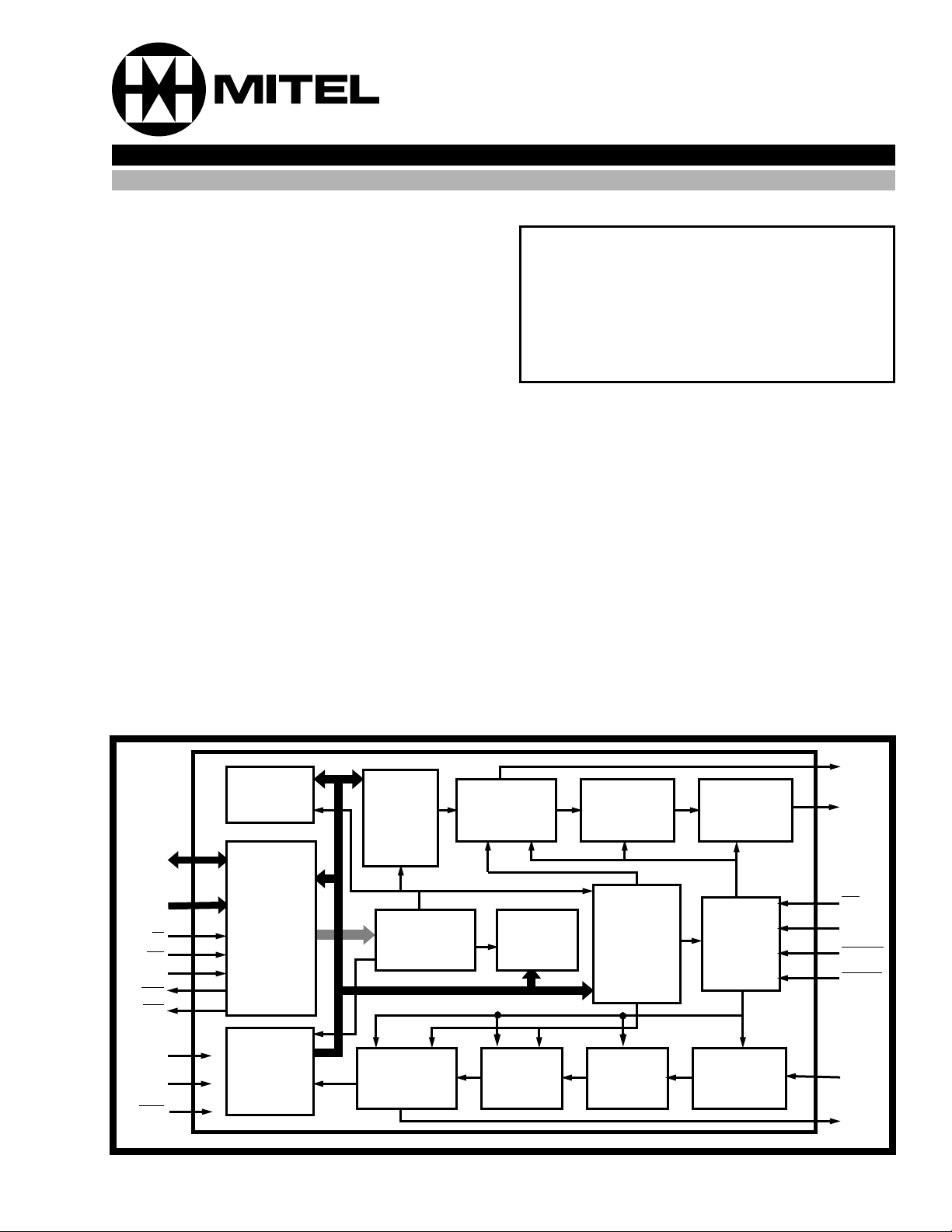
Figure 1 - Functional Block Diagram
3-61
MT8952B ISO-CMOS
TxCEN
RxCEN
CDSTo
CDSTi
R/
VSS
1
2
3
4
5
WD
6
IRQ
7
A0
8
A1
9
A2
10
A3
11
CS
12
E
13
W
14
28 PIN PDIP/CERDIP/SOIC
28
27
26
25
24
23
22
21
20
19
18
17
16
15
VDD
RST
F0i
CKi
TEOP
REOP
D7
D6
D5
D4
D3
D2
D1
D0
WD
IRQ
A0
A1
A2
A3
CS
CDSTi
4
5
6
7
8
9
10
11
12
E
28 PIN PLCC
CDSTo
RxCEN
3
2
•
13
14
W
R/
VSS
TxCEN
VDD
1
28
15
16
D1
D0
RST
27
17
D2
F0i
26
18
D3
25
24
23
22
21
20
19
CKi
TEOP
REOP
D7
D6
D5
D4
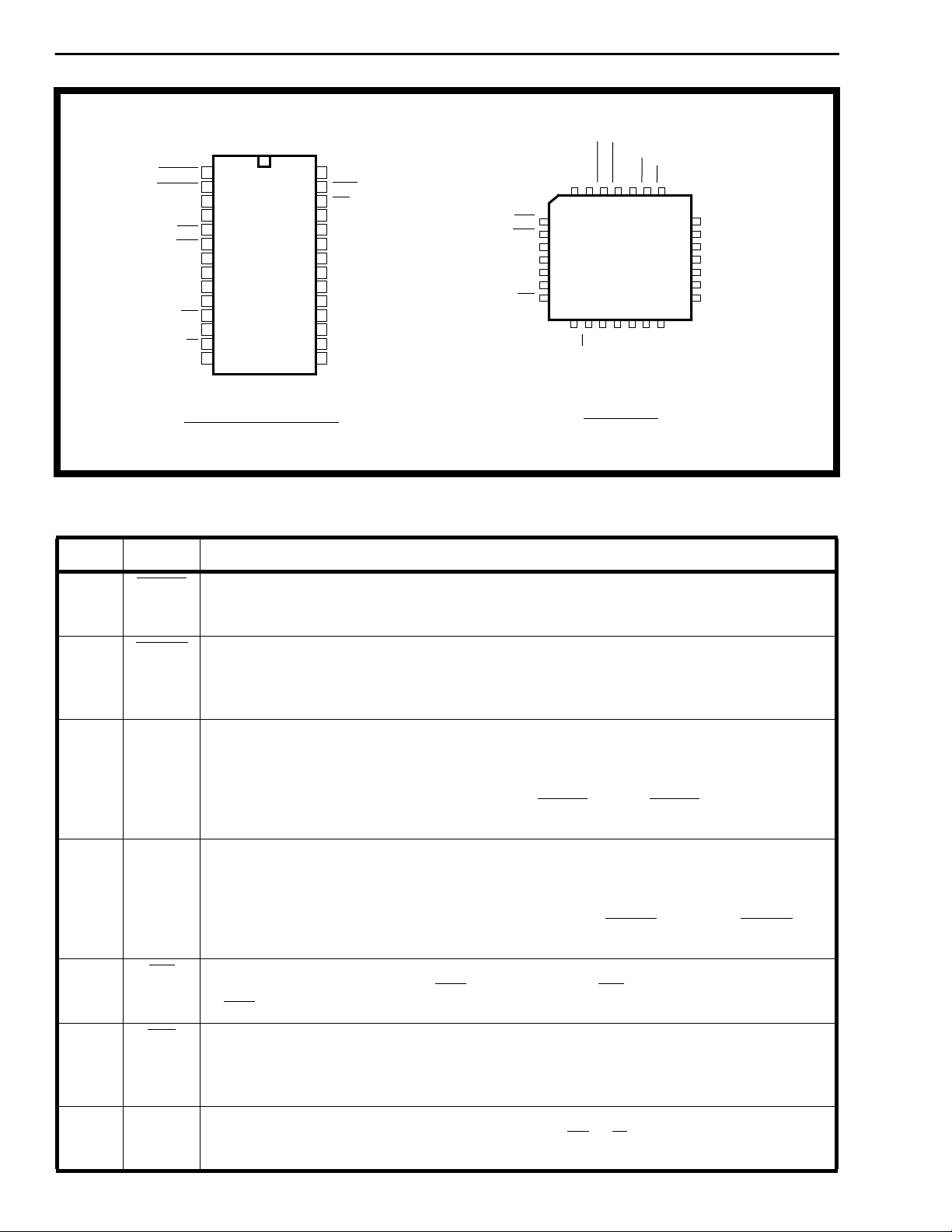
Figure 2 - Pin Connections
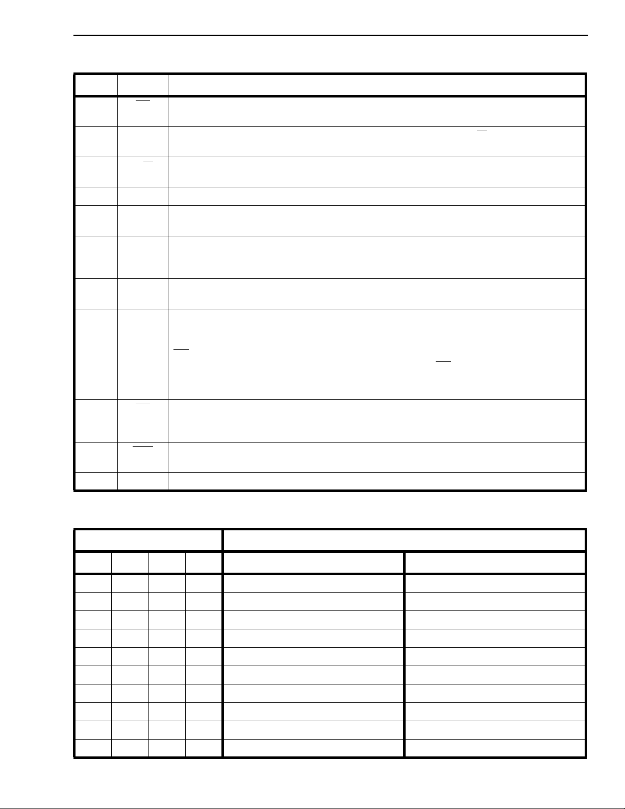
Pin Description
Pin No. Name Description
1 TxCEN T ransmit Cloc k Enable -This active LOW input enab les the transmit section in the External
Timing Mode. When LOW, CDSTo is enabled and when HIGH, CDSTo is in high impedance
state. If the Protocol Controller is in the Internal Timing Mode, this input is ignored.
2 RxCEN Receive Clock Enable - This active LOW input enables the receive section in the External
Timing Mode. When LOW, CDSTi is enabled and when HIGH, the clock to the receive
section is inhibited. If the Protocol Controller is in the Internal Timing Mode, this input is
ignored.
3 CDSTo C and D channel Output in ST-BUS format - This is the serial formatted data output from
the transmitter in NRZ form. It is in ST-BUS format if the Protocol Controller is in Internal
Timing Mode with the data in selected timeslots (0,2,3 and 4) and the C-channel information
in timeslot No. 1. If the Protocol Controller is in External Timing Mode, the formatted data is
output on the rising edge of the clock (CKi) when TxCEN LOW . IfTxCEN is HIGH, CDSTo is
in high impedance state.
4 CDSTi C and D channel Input in ST-BUS format - This is the serial formatted data input to the
receiver in NRZ form. It must be in ST-BUS format if the Protocol Controller is in Internal
Timing Mode with the input data in selected timeslots (0,2,3 and 4) and the C-channel
information in timeslot No.1. If the Controller is in External Timing Mode, the serial input
data is sampled on the falling edge of the clock CKi when RxCEN is LOW. If RxCEN is
HIGH, the clock to receive section is inhibited.
5 WD Watch-Dog Timer output - Normally a HIGH lev el output, going LO W if the Watchdog timer
times out or if the external reset (RST) is held LOW. The WD output remains LOW as long
as RST is held LOW.
6 IRQ Interrupt Request Output (Open Drain) - This active LOW output notifies the controlling
microprocessor of an interrupt request. It goes LOW only when the bits in the Interrupt
Enable Register are programmed to acknowledge the source of the interrupt as defined in
the Interrupt Flag Register.
7-10 A0-A3 Address Bus Inputs - These bits address the various registers in the Protocol Controller.
They select the internal registers in conjunction with CS, R/W inputs and E Clock. (Refer to
Table 1.)
3-62
ISO-CMOS MT8952B
Pin Description (continued)
Pin No. Name Description
11 CS Chip Select Input - This is an active LOW input enabling the Read or Write operation to
various registers in the Protocol Controller.
12 E Enable Clock Input - This input activates the Address Bus and R/W input and enables
data transfers on the Data Bus.
13 R/W Read/Write Control - This input controls the direction of data flow on the data bus. When
HIGH, the I/O buffer acts as an output driver and as an input buffer when LOW.
14 V
15-22 D0-D7 Bidirectional Data Bus - These Data Bus I/O ports allow the data transfer between the
23 REOP Receive End Of Packet (Output) - This is a HIGH going pulse that occurs for one bit
24 TEOP Transmit End Of Packet (Output) - This is a HIGH going pulse that occurs for one bit
25 CKi Clock Input (Bit rate clock or 2 x bit rate clock in ST-BUS format while in the Internal
26 F0i Frame Pulse Input - This is the frame pulse input in ST-BUS format to establish the
27 RST RESET Input - This is an active LOW Schmitt Trigger input, resetting all the registers
28 V
Ground (0 Volt).
SS
HDLC Protocol Controller and the microprocessor.
duration when a closing flag is detected on the incoming packets, or the incoming packet is
aborted, or when an invalid packet of 24 or more bits is received.
duration when a packet is transmitted correctly or aborted.
Timing Mode and bit rate Clock in the External Timing Mode) - This is the clock input
used for shifting in/out the formatted packets. It can be at bit rate (C2i) or twice the bit rate
(C4i) in ST-BUS format while the Protocol Controller is in the Internal Timing Mode.
Whether the clock should be C2i (typically 2.048 MHz) or C4i (typically 4.096 MHz) is
decided by the BRCK bit in the Timing Control Register. If the Protocol Controller is in the
External Timing Mode, it is at the bit rate.
beginning of the frame in the Internal Timing Mode. This is also the signal clocking the
watchdog timer.
including the transmit and receive FIFOs and the watchdog timer.
Supply (5 Volts).
DD
Address Bits Registers
A3 A2 A1 A0 Read Write
0 0 0 0 FIFO Status 0 0 0 1 Receive Data Transmit Data 0 0 1 0 Control Control 0 0 1 1 Receive Address Receive Address 0 1 0 0 C-Channel Control (Transmit) C-Channel Control (Transmit) 0 1 0 1 Timing Control Timing Control 0 1 1 0 Interrupt Flag Watchdog Timer 0 1 1 1 Interrupt Enable Interrupt Enable 1 0 0 0 General Status 1 0 0 1 C-Channel Status (Receive) -
Table 1. Register Addresses
3-63
MT8952B ISO-CMOS
Introduction
The MT8952B HDLC Protocol Controller handles bit
oriented protocol structure and formats the data as
per the packet switching protocol defined in the X.25
(Level 2) recommendations of the CCITT. It
transmits and receives the packeted data
(information or control) serially in a format shown in
Figure 3 , while providing the data transparency by
zero insertion and deletion. It generates and detects
the flags, various link channel states and the abort
sequence. Further, it provides a cyclic redundancy
check on the data packets using the CCITT defined
polynomial. In addition, it can generate and detect a
Go Ahead sequence and recognize a single byte
address in the received frame. There is also a
provision to disable the protocol functions and
provide transparent access to the serial bus through
the parallel port.
Frame Format
All frames start with an opening flag and end with a
closing flag as shown in Figure 3. Between these
two flags, a frame contains the data and the frame
check sequence (FCS).
FLAG DATA FIELD FCS FLAG
One Byte
n Bytes
(n ≥ 2)
Figure 3. Frame Format
Two
Bytes
One
Byte
address detection can be limited only to the upper
six bits by setting HIGH both RA6/7 and RxAD bits in
the Control Register.
Frame Check Sequence (FCS):
The 16 bits following the data field are the frame
check sequence bits. The generator polynomial is:
G(x)=x16+x12+x5+1
The transmitter calculates the FCS on all bits of the
data field and transmits after the data field and
before the end flag. The receiver performs a similar
computation on all bits of the received data and FCS
fields and the result is compared with FOB8
matches, the received data is assumed error free.
The error status of the received packet is indicated
by D7 and D6 bits in the FIFO Status Register.
Zero Insertion and Deletion:
The Protocol Controller, while sending either data
from the FIFO or the 16 bits FCS, checks the
transmission on a bit-by-bit basis and inserts a
ZERO after every sequence of five contiguous ONEs
(including the last five bits of FCS) to ensure that the
flag sequence is not simulated. Similarly the
receiver examines the incoming frame content and
discards any ZERO directly following the five
contiguous ONEs.
Abort:
Hex
. If it
Flag:
The flag is a unique pattern of 8 bits (01111110)
defining the frame boundary. The transmit section
generates the flags and appends them automatically
to the frame to be transmitted. The receive section
searches the incoming packets for flags on a bit-bybit basis and establishes frame synchronization. The
flags are used only to identify and synchronize the
received frame and are not transferred to the FIFO.
Data:
The data field refers to the Address, Control and
Information fields defined in the CCITT
recommendations. A valid frame should have a data
field of at least 16 bits. The first byte in the data field
is the address of the frame. If RxAD bit in the
Control Register is HIGH, the incoming packet is
recognized only if the address byte matches the byte
stored in the Receive Address Register or the
address byte is the All-Call Address (all ONEs). The
LSB of the Receive Address Register is set LOW
permanently and the comparison is done only on
upper seven bits of the received address byte. The
The transmitter aborts a frame by sending eight
consecutive ONEs. The FA bit in the Control
Register along with a write operation to the Transmit
Data Register enables the transmission of abort
sequence instead of the byte written to the register.
On the receive side, the ABRT bit in the General
Status Register is set whenever an abort sequence
(7 or more continuous 1’s) is received. The abort
sequence causes the receiver to abandon whatever
it was doing and start searching for a start flag. The
FA bit in the Interrupt Status Register is set when an
abort sequence is received following a start flag and
at least four data bytes (minimum for a valid frame).
Interframe Time Fill and Link Channel States
When the HDLC Protocol Controller is not sending
packets, the transmitter can be in any of three states
mentioned below depending on the status of the
IFTF0 and IFTF1 bits in the Control Register. These
bits are also used to disable the protocol function to
provide the transparent parallel access to the serial
bus through the microprocessor port.
3-64

ISO-CMOS MT8952B
Idle state:
The Idle state is defined as 15 or more contiguous
ONEs. When the HDLC Protocol Controller is
observing this condition on the receiving channel,
the Idle bit in the General Status Register is set
HIGH. On the transmit side, the Protocol Controller
ends the Idle state when data is loaded into the
transmit FIFO.
Interframe time fill state:
The Protocol Controller transmits continuous flags
(7E
) in Interframe time fill state and ends this
Hex
state when data is loaded into the transmit FIFO.
Go Ahead state:
Go Ahead is defined by the 9 bit sequence
011111110 (7F
contiguous 7F’s appear as Go Aheads. Once the
transmitter is in ‘Go Ahead’ state, it will continue to
remain so even after the data is loaded into the
FIFO. This state can only be changed by setting the
IFTF bits in the Control Register to something other
than ‘GO Ahead’. The reception of this sequence is
indicated by GA bit in the General Status Register
and the Protocol Controller can generate an interrupt
if enabled to do so by the GA bit in the Interrupt
Enable Register.
followed by a ZERO), and hence
Hex
The serial port can be configured to operate in two
modes depending on the IC bit in the Timing Control
Register. It can transmit/receive the packets on
selected timeslots in ST- BUS format or it can,
using the enable signals (TxCEN and RxCEN),
transmit/receive the packets at a bit rate equal to CKi
clock input.
The microprocessor port allows parallel data
transfers between the Protocol Controller and a
6800/6809 system bus. This interface consists of
Data Bus (D0-D7), Address Bus (A0-A3), E Clock,
Chip Select (CS) and R/W control. The microprocessor can read and write to the various registers
in the Protocol Controller. The addresses of these
registers are given in Table 2. The IRQ is an open
drain, active LOW output indicating an interrupt
request to CPU. Control and monitoring of many
different interrupts that may originate from the
protocol controller is implemented by the Interrupt
Flag Register (IFR) and the Interrupt Enable
Register (IER). Specific events have been described
that set a bit HIGH in the Interrupt Flag Register.
Such an event does not necessarily interrupt the
CPU. To assert an interrupt (pull IRQ output LOW)
the bit in IER that coincides with the Interrupt Flag
Register must be set HIGH. The IRQ bit in the
General Status Register is the complement of IRQ
pin status. If an interrupt is asserted, this bit will be
set HIGH otherwise it will be LOW.
Transparent Data Transfer State:
The Protocol Controller, in this state, disables the
protocol functions defined earlier and provides bidirectional access to the serial bit streams through
the parallel port. Like other states, the transparent
data transfer can be selected in both timing modes.
Invalid Frames
Any frame shorter than 32 bits between the opening
and closing flags (corresponding to 16 bits of data
and 16 bits FCS) is considered invalid. The Protocol
Controller ignores the frame only if the frame length
is less than 24 bits between the flags. For frames of
length 24 to 32 bits, it transfers the data field to FIFO
and tags it as having bad FCS in the FIFO Status
Register.
Functional Description
The functional block diagram of the HDLC Protocol
Controller is shown in Figure 1. It has two ports.
The serial port transmits and receives formatted data
packets and the parallel port provides a
microprocessor interface for access to various
registers in the Protocol Controller.
TEOP and REOP Outputs:
The HDLC Protocol Controller provides two separate
signals TEOP & REOP indicating the end of packet
transmitted and received respectively. TEOP is a
HIGH going pulse for one bit duration asserted
during the last bit of the closing flag or Abort
sequence of the transmit packet. REOP is also a
HIGH going pulse occurring for one bit period when
a closing flag is received or an incoming packet is
aborted or an invalid packet of 24 or more bits is
detected. However, REOP is not generated for
invalid packets of length less than 24 bits. These
‘end of packet’ signals are useful in multiplexing
several data links on to a single HDLC Protocol
Controller.
Timing Modes
There are two timing modes the Protocol Controller
can be run in. These timing modes refer only to the
configuration of the serial port and are not related to
the microprocessor port.
Internal Timing Mode
The Internal Timing Mode is intended for an easy
interface to various products using ST-BUS
3-65
MT8952B ISO-CMOS
architecture, particularly MITEL’s Digital Network
Interface Circuit (DNIC - MT8972). The data/packets
are shifted in/out serially in ST-BUS format using the
timing signals F0i and C2i/C4i. In addition to framing
the data, the Protocol Controller reserves one
channel (channel-1) on the ST-BUS for carrying
control information (C-channel) and this timeslot can
not be used for the packetized data. While the
Protocol Controller is in the Internal Timing Mode,
the clock input CKi can be either at the bit rate or at
2bit rate depending on the BRCK bit in the Timing
Control Register as shown in Table 2.
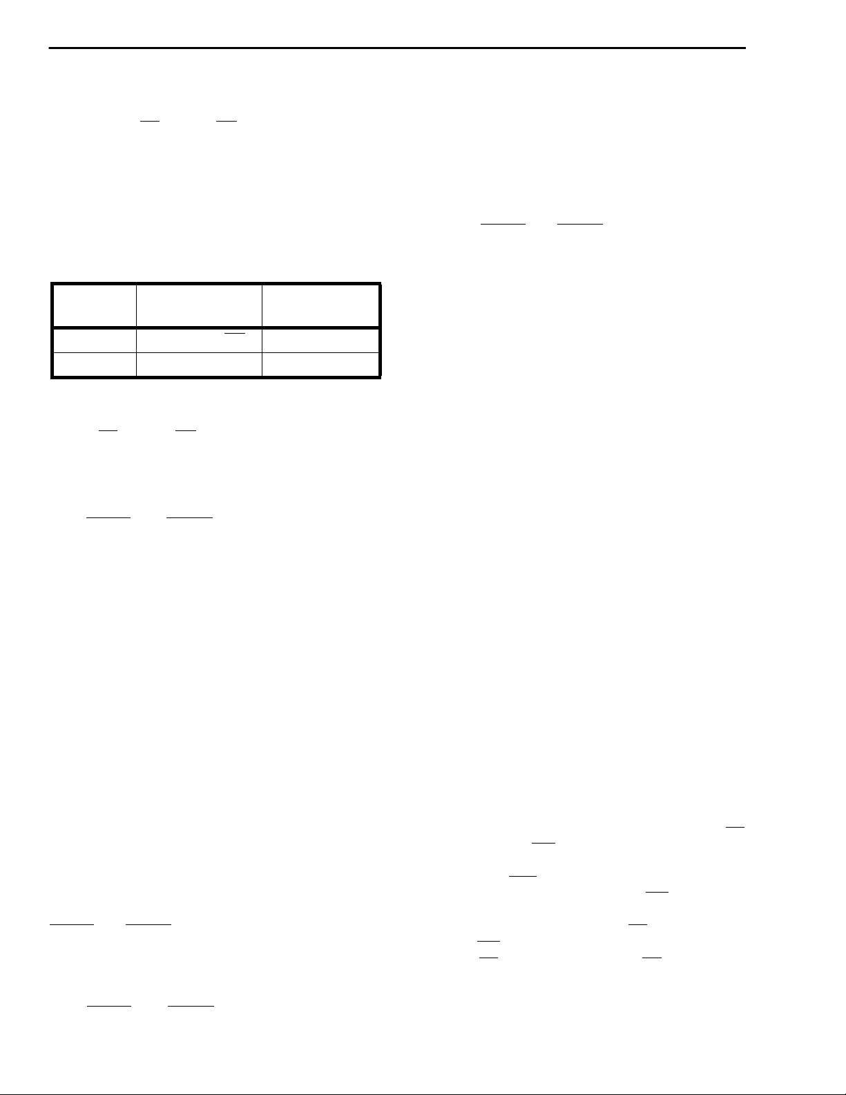
BRCK Bit CKi Input
0 4.096 MHz/C4i 2.048 Mbps 1 2.048 MHz/C2i 2.048 Mbps
Table 2. Output Bit Rate In Internal Timing Mode
The Protocol Controller uses the ST-BUS timing
signals F0i and C2i/C4i, and enables the transmitter
and receiver sections in the appropriate timeslots
as determined by TC0-TC3 bits in the Timing
Control Register.
The TxCEN and RxCEN inputs are ignored in this
mode.
C-Channel Interface
This is a separate control channel (C-channel)
interface relevant only in the Internal Timing Mode.
The data stored in the C-Channel Control Register is
shifted out during the channel-1 timeslot of the
outgoing ST-BUS (CDSTo) and the C1EN bit in the
Timing Control Register enables the transmission.
The transmission of C-Channel is independent of
packet/data transmission. The data received on
channel-1 of the incoming ST-BUS (CDSTi) is shifted
into the C-Channel Status Register independently
and it is updated continuously.
Both the C-channel registers are accessible by the
accompanying CPU through the parallel port.
External Timing Mode
In the External Timing Mode, the transmit and
receive sections are enabled independently by
TxCEN and RxCEN control inputs and the formatted
data packets are shifted in/out serially at a rate equal
to the clock frequency on CKi. The output is
transmitted on the rising edge and the receiver
samples the input on the falling edge of the clock.
The TxCEN and RxCEN controls are independent
Output Data
Rate
and asynchronous and have effect only after the
current bit in the packet is transmitted/received.
Although the protocol controller provides the
packetized data on a limited number of channels on
the ST-BUS while operating in the Internal Timing
Mode, it can packetize the data on any or all the
channels of the ST-BUS if it is operated in the
External Timing Mode with appropriate enable
signals on TxCEN and RxCEN.
Transparent Data Transfer
By setting the IFTF bits in the Control Register
appropriately, the protocol functions can be disabled.
This provides a bidirectional access to the serial port
through the microprocessor interface, with 19 byte
deep FIFO in each direction. The transparent data
transfer facility functions in bytewide format and is
available in both timing modes except when the
timing control bits are set for one bit/frame during the
Internal Timing Mode.
The transmit data is shifted out serially on CDSTo
and the operation being bytewide, only the least
significant bits of each byte loaded are transmitted, if
the timing control bits are set to select 2, 6 or 7 bits/
frame. When the transmit FIFO is empty, the last
byte or the portion the last byte, written to the FIFO
is transmitted repeatedly. Similarly the serial data on
CDSTi is shifted in and converted to bytewide
format. In case the timeslot selected is 2, 6 or 7 bits/
frame, the reception involves only the most
significant bits of each byte.
It should be noted that none of the protocol related
status or interrupt bits are applicable in transparent
data transfer state. However, the FIFO related status
and interrupt bits are pertinent and carr y the same
meaning as they do while performing the protocol
functions.
Watchdog Timer
This is a fixed eleven stage binary counter with F0i
as the input and WD as the output from the last
stage. This counter can be reset either by the
external input (RST) or by w riting XXX0 1010 to the
Watchdog Timer Register. The WD output is
normally HIGH and if the Watchdog Timer Register
is not written within 210cycles of F0i input after it is
reset, the WD output will go LOW for a period of 2
cycles of F0i. Even though the F0i input is not
required for formatting data in the External Timing
Mode, it is necessary for the operation of the
watchdog timer.
10
3-66
ISO-CMOS MT8952B
Order of Bit Transmission/Reception
The Least Significant Bit (LSB) corresponding to D0
on the data bus is transmitted first on the serial
output (CDSTo). On the receiving side, the first bit
received on the serial input (CDSTi) is considered as
the LSB and placed on D0 of the data bus.
Registers
There are several registers in the HDLC Protocol
Controller accessible to the associated microprocessor via the data bus. The addresses of these
registers are given in Table 1 and their functional
details are given below.
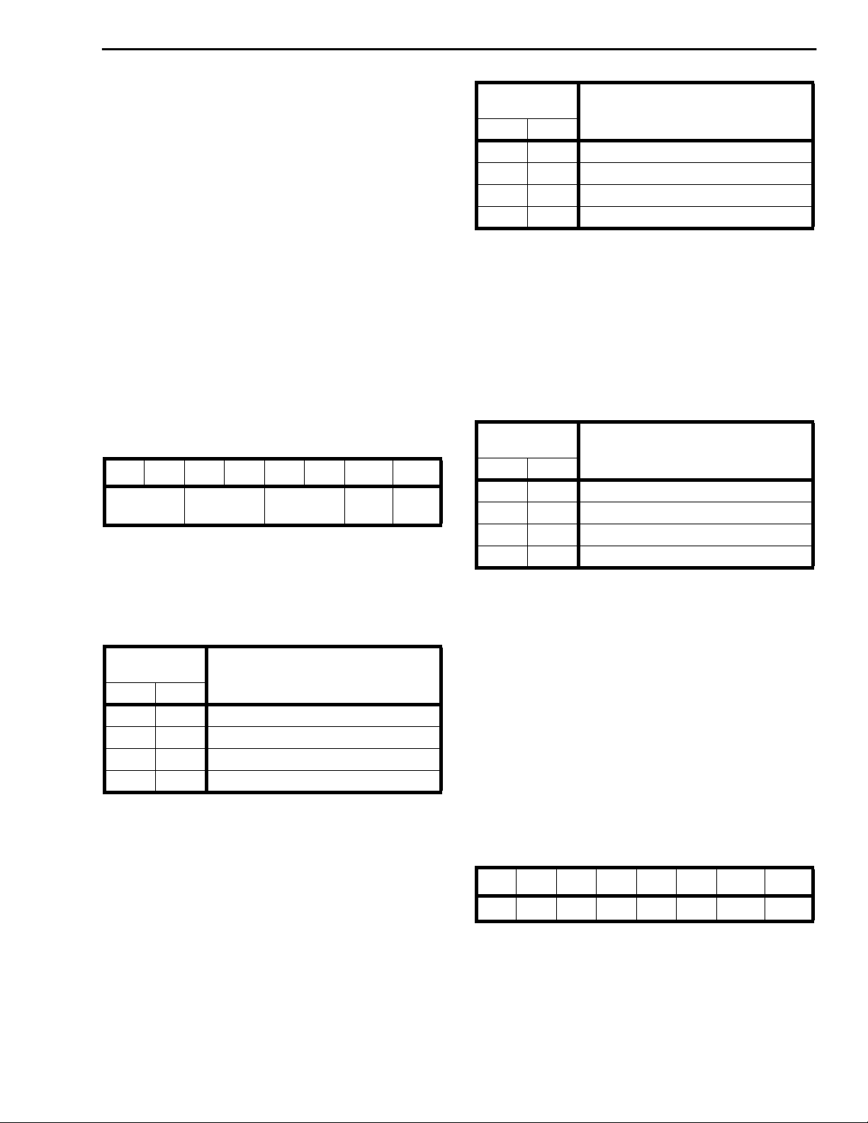
FIFO Status Register (Read):
This register (Figure 4) indicates the status of
transmit and receive FIFOs and the received byte as
described below.
D7 D6 D5 D4 D3 D2 D1 D0
Rx Byte
Status
Rx Byte Status: These two bits (D7 and D6) indicate
the status of the received byte ready to be read from
the receive FIFO. The status is encoded as shown in
Table 3.
Rx Byte
Status Bits
D7 D6
0 0 Packet Byte
0 1 First Byte
1 0 Last Byte (Good FCS)
1 1 Last Byte (Bad FCS)
Rx FIFO Status: These bits (D5 and D4) indicate the
status of receive FIFO as given by Table 4. The Rx
FIFO status bits are not updated immediately after
an access of the Rx FIFO (a read from the
microprocessor port, or a write from the ser ial port),
to avoid the existence of unrecoverable error
conditions.
Rx FIFO
Status
Figure 4 - FIFO Status Register
Table 3. Received Byte Status
Tx FIFO
Status
Status
LOW LOW
Rx FIFO
Status Bits
D5 D4
0 0 Rx FIFO Empty
0 1 Less than or equal to 14 bytes
1 0 Rx FIFO Full
1 1 Greater than or equal to 15 bytes
Table 4. Receive FIFO Status
updated. When in internal 4.096 MHz timing mode,
the MT8952B must receive four falling edges of the
C4i clock before the Rx FIFO status bit will be
updated (see the section on Receive Operation Normal Packets).
Tx FIFO Status: These two bits (D3 and D2) indicate
the status of transmit FIFO as shown in Table 5.
Tx FIFO
Status Bits
D3 D2
0 0 Tx FIFO Full
0 1 Greater than or equal to 5 bytes
1 0 Tx FIFO Empty
1 1 Less than or equal to 4 bytes
Table 5. Transmit FIFO Status
The Tx FIFO status bits are updated in the same
manner as the Rx FIFO bits, except that in external
timing mode, and in internal 2.048 Mbps timing
mode, the Tx FIFO status bits are updated after two
falling edges of the CKi or the C2i signal (see the
section on Transmit Operation - Normal Packets).
Receive Data Register (Read):
Reading the Receive Data Register (Figure 5) puts
the first byte from the receive FIFO on the data bus.
The first bit of the data received on the serial input
(CDSTi) is considered to be the LSB and is available
on D0 of the data bus.
D7 D6 D5 D4 D3 D2 D1 D0
RD7 RD6 RD5 RD4 RD3 RD2 RD1 RD0
Figure 5 - Receive Data Register
Status
Status
When in external timing mode, the MT8952B must
receive two falling edges of the clock signal at the
CKi input before the Rx FIFO status bits will be
updated. When in internal 2.048 MHz timing mode,
the MT8952B must receive two falling edges of the
C2i clock before the Rx FIFO status bits will be
Transmit Data Register (Write):
Writing to Transmit Data Register (Figure 6) puts the
data present on the data bus into the transmit FIFO.
The LSB (D0) is transmitted first.
3-67
 Loading...