MITEL MT8931CP, MT8931CC, MT8931CE Datasheet
CMOS ST-BUS FAMILY
MT8931C
Subscriber Network Interface Circuit
Preliminary Information
Features
• ETS 300-012, CCITT I.430 and ANSI T1.605
S/T interface
• Full-du plex 2B+ D, 19 2 kbi t/s tra nsmi ssio n
• Link acti vation/ deac tivat ion
• D-chann el acce ss cont entio n res olutio n
• Point-to-p oint, point-to- mu ltipo int and st ar
configurat ions
• Master (NT) /Slave (TE) mo des of operati on
• Exceeds lo op len gth re quire ments
• Comple te loopb ack t es ting capa bi lities
• On chip HDLC D-c han nel pro tocol ler
• 8 bit Motorola/Intel microprocessor interface
• Microproc essor-c ontrol led op eration
• Mitel ST-BUS interface
• Low power CM OS tech nolog y
• Single 5 vol t pow er su pply
Applications
• ISDN NT1
• ISDN S or T interf ace
• ISDN Terminal Adaptor (TA)
• Digital sets (TE1) - 4 wire ISDN interface
• Digital PABXs, Digital Line Cards (NT2)
ISSUE 1 May 1995
Ordering Information
MT8931CC 28 Pin Ceramic DIP
MT8931CE 28 Pin Plastic DIP
MT8931CP 44 Pin PLCC
-40°C to +85°C
Description
The MT8931C Subscriber Network Interface Circuit
(SNIC) implements the ETSI ETS 300-012, CCITT
I.430 and ANSI T1.605 Recommendations for the
ISDN S and T reference points. Providing point-topoint and point-to-multipoint digital transmission, the
SNIC may be used at either end of the subscriber
line (NT or TE).
An HDLC D-channel protocoller is included and
controlled through a Motorola/Intel microprocessor
port.
The MT8931C is fabricated in Mitel’s CMOS
process.
DSTi
DSTo
F0od
C4b
F0b
STAR/Rsto
XTAL1/NT
XTAL2/NC
Rsti
ST-BUS
Interface
Timing
and
Control
HALF AD0-7 R/W/WR DS/RD
D-channel Priority
Mechanism
PLL
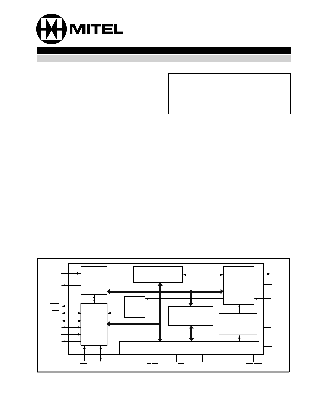
Figure 1 - Functional Block Diagram
HDLC
Transceiver
Microprocessor Interface
AS/ALE CS
S-Bus
Link
Interface
Link
Activation
Controller
LTx
VBias
LRx
VDD
VSS
IRQ/NDA
9-73
MT8931C Preliminary Information
HALF
C4b
F0b
F0od
DSTi
DSTo
XTAL2/ NC
XTAL1/ N T
/WR
R/W
DS/RD
AS/ALE
CS
IRQ/NDA
VSS
1
2
3
4
5
6
7
8
9
10
11
12
13
14
28 PIN PDIP/CERDIP
28
27
26
25
24
23
22
21
20
19
18
17
16
15
VDD
VBias
LTx
LRx
STAR/Rsto
Rsti
AD7
AD6
AD5
AD4
AD3
AD2
AD1
AD0
F0od
DSTi
DSTo
NC
NC
NC
XTAL2/NC
XTAL1/NT
NC
/WR
R/W
DS/RD
NCNCC4b
F0b
65432 44434241
7
8
9
10
11
12
13
14
15
16
17
CS
NC
AS/ALE
44 PIN PLCC
NC
HALF
VDD
1
231819202122 24 25 262728
NC
AD0
VSS
IRQ/NDA
VBias
AD1
LTx
NC
LRx
40
NC
39
STAR/Rsto
38
37
Rsti
NC
36
35
AD7
34
AD6
33
NC
32
AD5
31
AD4
30
AD3
29
NC
NC
NC
AD2
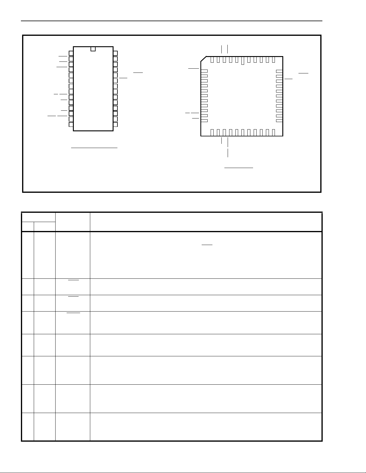
Figure 2 - Pin Connections
Pin Description
Pin #
DIP PLCC
12 HALFHALF Input/O utpu t : this is an input in NT mode and an out put in TE mode ident ifying
Name Description
which half of the S-interface fram e is currently being written/rea d over the ST-BUS
(HALF = 0 sampled on the falling edge of C4b
within the frame pulse low window,
identifies the informa tio n to be transmitted/ received in the first half of the S-Bus frame
while HALF= 1 identifi es the informa tion to be transmitted/ received into the second half
of the S-Bus frame). Tying this pin to V
or VDD in NT mode will allow the device to free
SS
run. This signal can also be accessed from the ST-BUS C-channel.
23 C4b
4.096 MHz Clock: a 4.096 MHz ST-BUS Data Clock input in NT mode.
In TE mode an output 4.096 MHz clock phase-locked to the line data signal.
34 F0b
Frame Pulse: an active low frame pulse inp ut indicating the beginni ng of active STBUS channel time s in NT mode. Fram e pulse outp ut in TE mo de.
47 F0od
Delayed Fram e Pulse Ou tput: an active low delayed frame pulse out put indicat ing
the end of active ST-BUS channels for this device. Can be used to daisy chain
to other ST-BUS devices to share an ST-BUS stream.
58 DSTiData ST-BUS Input: a 2048 kbit/s serial PCM/data ST-BUS input with D, C, B1, and B2
channels assigned to the first four timeslots. These channe ls contain dat a to be
transmitted on the line and chip control informat ion.
69 DSToData ST -BUS Output: a 2048 kbit/s serial PCM/dat a ST-BUS output with D, C, B1 and
B2 channels assigned to the first four timeslots, respectivel y. The remaining timeslots
are placed into high impedance. These channels contain data received from the line
and chip status informati on.
7 13 XTAL2/IC Crystal 2/Internal Connection: in TE mode, XTAL1 and XTAL2 are to be connected to
an external 4.096 MHz parallel resonant crystal for the on-chip oscillator.
If XTAL1 is connected directly to a 4.096 MHz clock, this pin must be left unconnected.
In NT mode, this pin must be left unconnecte d.
8 14 XTAL1/NT Crystal 1/Netwo rk Termination Mode Select Inpu t: for TE mode mode selection, a
4.096 MHz crystal is to be connected between the XTAL1 and XTAL2 pins, or a 4.096
MHz clock can be connected directly to XTAL1. For NT mode selection, this pin must
be tied to VDD. A pull-up resistor is needed when driven by a TTL device.
9-74

Preliminary Information MT8931C
Pin Description (continued)
Pin #
DIP PLCC
916 R/W/WR Read/Write or Write Input: defines the data bus transfer as a read (R/W=1) or a write
10 17 DS/RD
11 19 AS/ALE Address Strobe/Address Latch Enable Input: in Motorola bus mode the falling edge
12 20 CS
13 21 IRQ
14 22 V
15-2224-26,
30-32,
34-35
Name Description
(R/W
=0) in Motorola bus mode. Redefined to WR in Intel bus mode.
Data Strobe/Read Input: active high input indicat es to the SNIC that valid data is on
the bus during a write operatio n or that th e SNIC must output data during a read
operation in Motorola bus mode. Redefined to RD
in Intel bus mode.
is used to strobe the address into the SNIC during microprocessor access. Redefined
to ALE in Intel bus mod e.
Chip Select Input: active low, used to select the SNIC for microprocessor access.
Interrupt Reques t (Open Drai n Outpu t): an outp ut indicati ng an unmasked HDLC
interrupt. The interrupt remains active unti l the microprocessor clears it by reading the
HDLC Interrupt Status Regist er. This interrupt source is enabled with B2=0 of Master
Control Register.
NDA
New Data Available (Open Drain Output): an active low output signal indicating
availabilit y of new data from the S-Bus. This signal is selecte d with B2=1 of Master
Control Register. This pin must be tied to V
SS
Ground .
with a 10kΩ resistor.
DD
AD0-7 Bidirectional Address/Data Bus: electrically and logically compatible to either Intel or
Motorola micro-bus specificat ions. If DS/RD
the chip operates to Motorola specs. If DS/RD
mode is selected. Taking Rsti
low sets Motorola mo de.
is low on the rising edge of AS/ALE then
is high on the rising edge of AS/ALE Intel
23 37 Rsti
Reset Input: Schmitt trigger reset input. If ’0’, sets all control registers to the default
conditions, resets activation stat e machines to the deactivat ed stat e, resets HDLC,
clears the HDLC FIFO‘ s. Sets the micropo rt to M otorol a bus m ode.
24 38 STAR/Rsto
Star/Reset (Open Drain Output): 192kb it/s Rx data outp ut fixed relati ve to the STBUS timebase. A group of NTs, in fixed timing mode, can be wire or’ed toget her to
create a Star configuratio n. Active low rese t output in TE mode indicat ing 128
consecutive marks have been received. Can be connected directly to Rsti
to reset all TEs on the bus. This pin must be tied to V
with a 10 kΩ resistor.
DD
to allow NT
25 40 LRx Receive Line Signal Input: this is a high impedance input for the pseudoternary line
signal to be connected to the line through a 2:1 ratio transformer. See Figures 20 and
21. A DC bias level on this input equal to V
must be maintained.
Bias
26 42 LTx Transmit Line Signal Output: this is a current source output designed to drive a
nominal 50 ohm line through a 2:1 ratio transformer. See Figures 20 and 21.
27 43 V
28 44 V
1,5-6,10-
12,1 5,18,
23,27-
29, 33,
36, 39,
41
Bias
DD
NC No Connection.
Bias Voltage: analog ground for Tx and Rx transformers. This pin must be decoupled
to V
through a 10µF capacitor with good high frequency characteristic s.
DD
Power Sup pl y Input.
9-75
MT8931C Preliminary Information
Functional Description
The MT8931C Subscriber Network Interface Circuit
(SNIC) is a multifunction transceiver providing a
complete interface to the S/T Reference Point as
specified in ETS 300-012, CCITT Recommendation
I.430 and ANSI T1.605. Implementing both
point-to-point and point-to-multipoint voice/data
transmission, the SNIC may be used at either end of
the digital subscriber loop. A programmable digital
interface allows the MT8931C to be configured as a
Network Termination (NT) or as a Terminal
Equipment (TE) device.
The SNIC supports 192 kbit/s (2B+D + overhead) full
duplex data transmission on a 4-wire balanced
transmission line. Transmission capability for both B
and D channels, as well as related timing and
synchronization functions, are provided on chip. The
signalling capability and procedures necessary to
enable customer terminals (TEs) to be activated and
deactivated, form part of the MT8931C’s
functionality. The SNIC handles D-channel resource
allocation and prioritization for access contention
resolution and signalling requirements in passive bus
line configurations. Control and status information
allows implementation of mainten-ance functions
and monitor ing of the dev ice and the subscr iber loop .
An HDLC transceiver is included on the SNIC for link
access protocol handling via the D-channel.
Depacketized data is passed to and from the
transceiver via the microprocessor port. Two 19 byte
deep FIFOs, one for transmit and one for receive,
are provided to buffer the data. The HDLC block can
be set up to transmit or receive to/from either the
S-interface port or the ST-BUS port. Further, the
transmit destination and receive source can be
independently selected, e.g., transmit to S-interface
while receiving from ST-BUS. The transmit and
receive paths can be separately enabled or disabled.
Both, one and two byte address recognition is
supported by the SNIC. A transparent mode allows
data to be passed directly to the D channel without
being packetized.
A block diagram of the MT8931C is shown in Figure
1. The SNIC has three interface ports: a 4-wire
CCITT compatible S/T interface (subscriber loop
interface), a 2048 kbit/s ST-BUS serial port, and a
general purpose parallel microprocessor port. This
8-bit parallel port is compatible with both Motorola or
Intel microprocessor bus signals and timing.
The three major blocks of the MT8931C, consisting
of the system serial interface (ST-BUS), HDLC
transceiver, and the digital subscriber loop interface
(S-interface) are interconnected by high speed data
busses. Data sent to and received from the
S-interface port (B1, B2 and D channels) can be
accessed from either the parallel microprocessor
port or the serial ST-BUS port. This is also true for
SNIC control and status information (C-channel).
Depacketized D-channel information to and from the
HDLC section can only be accessed through the
parallel microprocessor port.
S-Bus Interface
The S-Bus is a four wire, full duplex, time division
multiplexed transmission facility which exchanges
information at 192 kbit/s rate including two 64 kbit/s
PCM voice or data channels, a 16 kbit/s signalling
channel and 48 kbit/s for synchronization and
overhead. The relative position of these channels
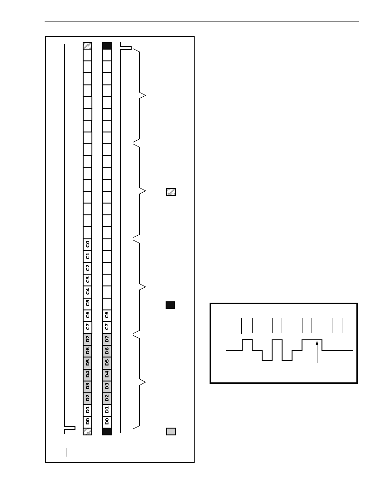
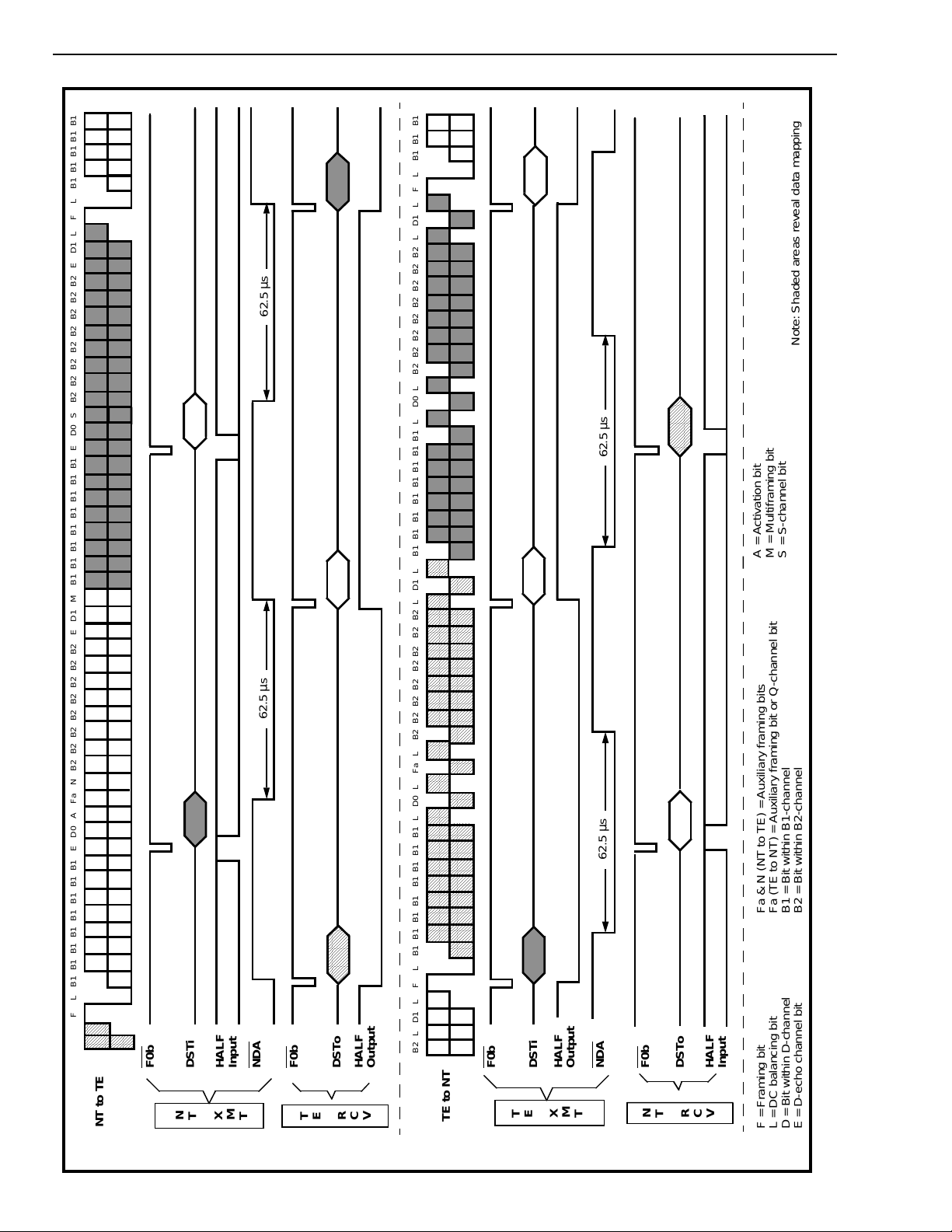
with respect to the ST-BUS is shown in Figures 4
and 5.
The SNIC makes use of the first four channels on the
ST-BUS to transmit and receive control/status and
data to and from the S-interface port. These are the
B, D and C-channels (see Figure 4).
9-76
HALF
C4bi
F0bi
F0od
DSTi
DSTo
Cmode
NT
/WR
R/W
DS/RD
AS/ALE
CS
IRQ/NDA
VSS
NT MODE TE MODE
1
2
3
4
5
6
7
8
9
10
11
12
13
14
28
27
26
25
24
23
22
21
20
19
18
17
16
15
VDD
VBias
LTx
LRx
STAR
Rsti
AD7
AD6
AD5
AD4
AD3
AD2
AD1
AD0
HALF
C4bo
F0bo
F0od
DSTi
DSTo
XTAL2
XTAL1
/WR
R/W
DS/RD
AS/ALE
CS
IRQ/NDA
VSS
1
2
3
4
5
6
7
8
9
10
11
12
13
14
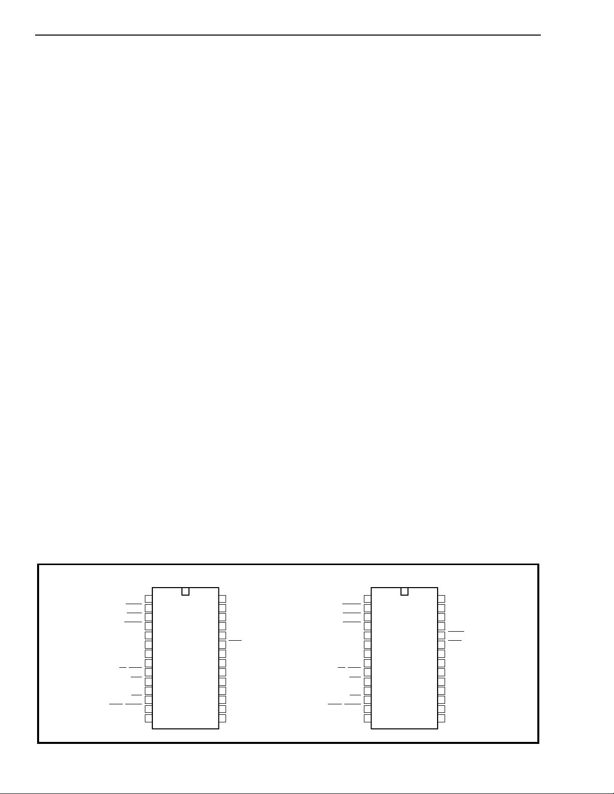
Figure 3 - SNI C Pi n Co nn ec tion s
28
27
26
25
24
23
22
21
20
19
18
17
16
15
VDD
VBias
LTx
LRx
Rsto
Rsti
AD7
AD6
AD5
AD4
AD3
AD2
AD1
AD0
Preliminary Information MT8931C
A
A
AAAA
A
A
AAAA
A
A
A
The B1 and B2 channels each have a bandwidth of
AAA
AAA
AAA
AAA
64 kbit/s and are used to carry PCM voice or data
across the network.
The D-channel is primarily intended to carry
signalling information for circuit switching through
the ISDN network. The SNIC provides the capability
of having a 16 kbit/s or full 64 kbit/s D-channel by
allocating the B1-channel timeslot to the D-channel.
Access to the depacketized D-channel is only
granted through the parallel microprocessor port.
The C-channel provides a means for the system to
control and monitor the functionality of the SNIC.
This control/status channel is accessed by the
system through the ST-BUS or microprocessor
port. The C-channel provides access to two
registers which provide complete control over the
state activation machine, the D-channel priority
mechanism as well as the various maintenance
functions. A deta il e d de scr ip ti on o f th es e regis te r s is
discussed in the microprocessor port interface.
AAA
AAA
B1 B1 B1 B1 B1 B1 B1 B1 B2 B2 B2 B2 B2 B2 B2 B2
C7 C6 C5 C4 C3 C2 C1 C0
D0 D1 D2 D3 D4 D5 D6 D7
B1 B1 B1 B1 B1 B1 B1 B1 B2 B2 B2 B2 B2 B2 B2 B2
C7 C6 C5 C4 C3 C2 C1 C0
D0 D1 D2 D3 D4 D5 D6 D7
Line Code
The line code used on the S-interface is a Pseudo
ternary code with 100% pulse width as seen in
Figure 5 below. Binary zeros are represented as
marks on the line and successive marks will
alternate in polarity.
Channel 1 (C) Channel 2 (B1) Channel 3 (B2)Channel 0 (D)
BINARY
VALUE
0100010011
LINE
SIGNAL
Violation
Figur e 5 - Alte rn at e Ze ro I nve rsi on L ine Co de
A mark which does not adhere to the alternating
polarity is known as a bipolar violation.
Only val id w ith 64 kbit/s D-channel Output in hig h im pe dance state Don’t car e
F0b
DSTi
DSTo
F0od
Figure 4 - ST-BUS Chan nel Ass ignm ent
9-77
MT8931C Preliminary Information
A
A
A
A
A
A
A
A
A
A
A
A
A
A
A
A
A
A
A
A
A
A
A
A
A
A
A
A
A
A
A
A
A
A
A
A
A
A
A
A
A
A
A
A
A
A
A
A
A
A
A
A
A
A
A
A
A
A
A
A
A
A
A
A
A
A
A
A
A
A
A
A
A
A
A
A
A
A
A
A
A
A
A
A
A
A
A
A
A
A
A
A
A
A
A
A
A
A
A
A
A
A
A
A
A
A
A
A
A
A
A
A
A
A
A
A
A
AA
A
A
A
A
A
A
A
B1 B1B1
62.5 µs
Note: Shaded areas reveal data mapping
B1
AAA
AAA
AAA
AAA
AAA
B2 L LD1 B1B1 B1B1 B1 B1 B1 L D0 L B2 B2 B2 B2B1 B2 B2 B2 B2 L D1 LB2 L LD1 LFB1B1 B1 B1 B1 B1 B1 L D0 L Fa LB1 B2 B2 B2 B2 B2 B2 B2 FL
AAA
AAA
AAA
AAA
AAA
AAA
AAA
AAA
AAA
AAA
AAA
AAA
AAA
AAA
AAA
AAA
AAA
AAA
AAA
AAA
AAA
AAA
AAA
AAA
AAA
AAA
AAA
AAA
AAA
AAA
AAA
AAA
AAA
AAA
AAA
AAA
AAA
AAA
AAA
AAA
AAA
AAA
AAA
AAA
AAA
AAA
AAA
AAA
AAA
AAA
AAA
AAA
AAA
AAA
AAA
AAA
AAA
AAA
AAA
AAA
AAA
AAA
AAA
AAA
AAA
AAA
AAA
AAA
AAA
AAA
AAA
AAA
AAA
AAA
AAA
AAA
AAA
AAA
AAA
AAA
AAA
AAA
AAA
AAA
AAA
AAA
AAA
AAA
B1 B1 B1B1 B1B1 EB1 D0 B2 B2 B2 B2 B2 B2 B2 B2 ES D1 L F L B1 B1FL B1B1 B1B1 B1B1 B1 E D0 A Fa N B2B2B2B2B1 B2 B2 B2 B2 E D1 M B1 B1 B1
62.5 µs
62.5 µs
A = Activation bit
M = Multiframing bit
S = S-channel bit
62.5 µs
Fa & N (NT to TE) = Auxiliary framing bits
Fa (TE to NT) = Auxiliary framing bit or Q-channel bit
Figure 5 - S-Bus Frame Structure and Functional Timing
B1 = Bit within B1 -channel
B2 = Bit within B2 -channel
AAA
AAA
AAA
A
DSTi
TEX
HALF
NDA
F0b
DSTo
HALF
Output
M
T
NTR
Input
V
C
F = Framing bit
L = DC balancing bit
D = Bit within D-channel
E = D-echo channel bit
F0b
NT to TE
9-78
NTX
Input
DSTi
HALF
NDA
F0b
DSTo
HALF
Output
T
M
TER
C
V
F0b
TE to NT

Preliminary Information MT8931C
Fram ing
The valid frame structure transmitted by the NT and
TE contains the following (refer Fig. 6):
NT to TE:
- Framing bit (F)
- B1 and B2 channels (B1,B2)
- DC balancing bits (L)
- D-channel bits (D0, D1)
- Auxiliary framing and N bit (Fa, N), N=Fa
- Activation bit (A)
- D-echo channel bits (E)
- Multiframing bit (M)
- S-channel bit
TE to NT:
- Framing bit (F)
- B1 and B2 channels (B1, B2)
- DC balancing bits (L)
- D-channel bits (D0, D1)
- Auxiliary framing bit (Fa) or Q-channel bit
The framing mechanism on the S-interface makes
use of line code violations to identify frame
boundaries. The F-bit violates the alternating line
code sequence to allow for quick identification of the
frame boundaries. To secure the frame alignment,
the next mark following the frame balancing bit
(L) will also produce a line code violation. If the
data following the balancing bit is all binary ones,
the zero in the auxiliary framing bit (Fa) or N-bit (for
the direction NT to TE) will provide successive
violations to ensure that the 14 bit criterion (13 bit
criterion in the direction TE to NT) specified in
Recommendations I.430 and T1.605 is satisfied. If
the B1-channel is not all binary ones, the first zero
following the L-bit will violate the line code sequence,
thus allowing subsequent marks to alternate without
bipolar violations.
The Fa and N bits can also be used to identify a
multiframe structure (when this is done, the 14 bit
criterion may not be met). This multiframe structure
will make provisions for a low speed signalling
channel to be used in the TE to NT direction
(Q-channel). It will consist of a five frame multiframe
which can be identified by the binary inversion of the
Fa and N-bit on the first frame and consequently on
every fifth frame of the multiframe. Upon detection
of the multiframe signal, the TE will replace the next
Fa-bit to be transmitted w ith th e Q -bi t.
The A-bit is used by the NT during line activation
procedures (refer to state activation diagrams). The
state of the A-bit will advise the TE if the NT has
achieved synchronization.
The E-bit is the D-echo channel. The NT will reflect
the binary value of the received D-channel into the
E-bits. This is used to establish the access
contention resolution in a point-to-multipoint
configuration. This is described in more detail in the
section of the D-channel priority mechanism.
The M-bit is a second level of multiframing which is
used for structuring the Q-bits. The frame with Mbit=1 identifies frame #1 in the twenty frame
multiframe. The Q-channel is then received as
shown in Table 1. All synchronization with the
multiframes must be performed externally.
FRAME # Q-BIT M-BIT
1Q11
6Q20
11 Q3 0
16 Q4 0
Table 1. Q-channel Allocation
Bit Order
When using the B-channels for PCM voice, the first
bit to be transmitted on the S-Bus should be the sign
bit. This complies with the existing telecom
standards which transmit PCM voice as most
significa nt b it fir st. However, if the B-c h an n e ls a r e to
carry data, the bit ordering must be reversed to
comply with the existing datacom standards (i.e.,
least significant bit first).
These contradicting standards place a restriction on
all information input and output through the serial
and parallel ports. Information transferred through
the serial ports, will maintain the integrity of the bit
order. Data sent to either serial port from the parallel
port, will transmit the least significant bit first.
Therefore, a PCM byte input through the
microprocessor port must be reordered to have the
sign bit as th e l e a st significant bit.
When the microprocessor reads D, B1 or B2 channel
data of either ST-BUS or S-bus serial port, the least
significant bit read is the first bit received on that
particular channel of either serial port.
The DC balancing bits (L) are used to remove any
DC content from the line. The balancing bit will be a
mark if the number of preceding marks up to the
previous balancing bit is odd. If the number of marks
is even, the L-bit will be a space.
The D-channel received on the serial ST-BUS ports
must be ordered with the least significant bit first as
shown in Figure 4. This also applies to the
D-channel directed to the ST-BUS from the
microprocessor port.
9-79
MT8931C Preliminary Information
The C-channel bit mapping from the parallel port to
the ST-BUS is organized such that the most
significa n t b it i s tra n smitted or rec e ive d fi rs t.
State Activation
The state activation controller activates or
deactivate s the SN IC in response to line activi ty or
external command. The controller is completely
hardware driven and need not be initialized by the
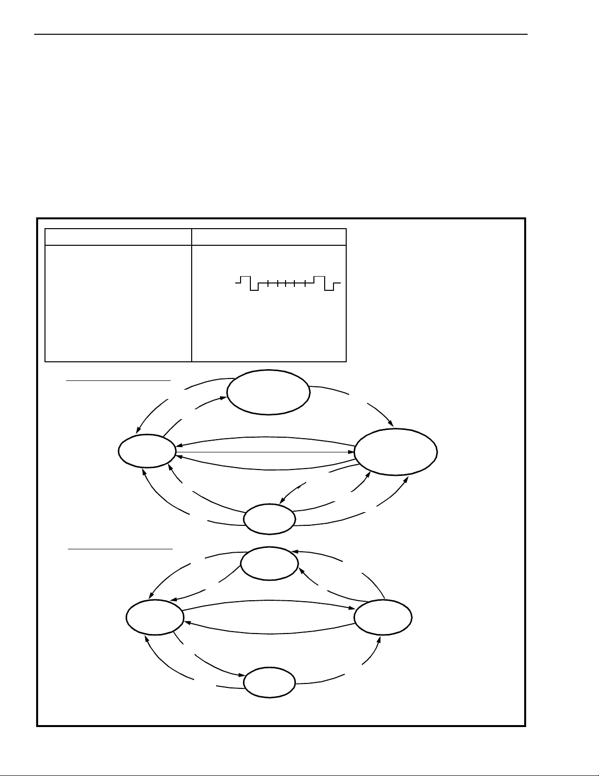
microprocessor. The state diagram for initialization
is shown in Figure 7.
Signals from NT to TE Signals from TE to NT
Info0
Info2
Info4
No Signal
Valid frame structure with
all B, D, D-echo and A bits
set to ‘0’
Valid frame with data in B,
D, D-echo channels. Bit A is
set to 1.
TE State Activati on Diag ram
DR = 1
Info0 No Signal
Info1 Continuous Signal of +‘0’, -‘0’
Info3 Valid frame with data in B & D
AR = 1
and six ‘1’s
Bits
Activation Request
send Info1 if BA = 0
send Info0 if BA = 1
The protocol used by the state activation controller is
defined as follows:
1) In the deactivated state, neither the NT nor TE
assert a signal on the line (Info0).
2) If the TE wa n ts to in i tia te a ctivation, it must begin
transmitting a continuous signal consisting of a
positive zero, a negative zero followed by six
ones (Info1).
3) Once the NT has detected Info1, it begins to
transmit Info2 which c onsists of an S-Bus frame
(2)
Where: BA
(1)
Note 1: signal is not timebase locked to NT.
Note 2: Sync/BA bit of the Status Register
Sync = 1
= Bus Activity
DR = Deactivation Request
AR = Activation Request
(2)
= Frame Sync Signal
Sync
A = Activation bit
Time out = 32 ms Timer Signal
is configured as Sync bit when
AR = 1 and DR = 0, or as BA bit
when AR = 0 or DR = 1. A change in
the state of the AR and/or DR bits
will cause a change in the function
of the Sync/BA bit in the following
ST-BUS frame.
Deactivated
send Info0
NT State Activation Diagram
Pending
Activation
send Info2
DR = 1
BA = 0
BA = 1
AR = 1
Sync = 1
Sync = 0
BA = 0
Sync = 1
DR = 1
Activated
send Info3
Deactivated
send Info0
DR = 1
AR = 1
Activated
send Info4
A = 1 &
Sync = 1
BA =0
Synchronized
send Info3 if Sync = 1
send Info0 if Sync = 0
Sync = 0
A = 0
Time out
Pending
Deactivation
Send Info0
DR = 1
9-80
Figure 7 - Link Activation Protocol, State Diagram
Preliminary Information MT8931C
with zeros in the B and D-channel and the
activation b it (A-bit) set to ze ro .
4) As soon as the TE synchronizes to Info2, it
responds with a valid S-Bus frame with data in
the B1, B2 and D-channel (Info3).
5) The NT will then transmit a valid frame with data
in the B1, B2 and D-channel. It will also set the
activation bit (A) to binary one once
synchroniz a ti on to Info3 is a ch i e ve d .
If the NT wishe s to initi a te th e a ct iva ti o n, step s 2 and
3 are ignored and the NT starts sending Info2. To
initiate a deactivation, either end begins to send
Info0 (Idle li ne) .
D-channel Priority Mechanism
The SNIC contains a hardware priority mechanism
for D-channel contention resolution. All TEs
connected in a point-to-multipoint configuration are
allocated the D-channel using a systematic
approach. Allocation of the D-channel is
accomplished by monitoring the D-echo channel
(E-bit) and incrementing the D-channel priority
counter with every consecutive one echoed back in
the E bit. Any zero found on the D-echo channel will
reset the priority counter.
There are two classes of priority within the SNIC,
one user accessible and the other being strictly
internal. The user accessible priority selects the
class of operation and has precedence over the
internal priority. The latter (internal priority), will
select the leve l of priority within ea ch class (i.e., th e
internal priority is a subsection of the user accessible
priority). User accessible priori ty selects the terminal
count as 8/9 or 10/11 consecutive ones on the E-bit
(8 being high priority while 10 being low priority).
The internal priority selects the terminal between 8
or 9 for high class and 10 or 11 for low class. The
first terminal equipment to attain the E-bit priority
count will immediately take control of the D-channel
by sending the opening flag. If more than one
terminal has the same priority, all but one of them will
eventually detect a collision. The TEs that detect a
collision will immediately stop trans-mitting on the Dchannel, generate an interrupt through the Dcoll bit,
reset the DCack bit on the next frame pulse, and
restart the counting process. The remainder of the
packet in the Tx FIFO is ignored.
NT
NT is operating in adaptive timing
TR is the line terminat ion re sistor = 100 Ω
NT is operating in fixed timing
TR is the line termination resistor = 100 Ω
T
R
NT
T
R
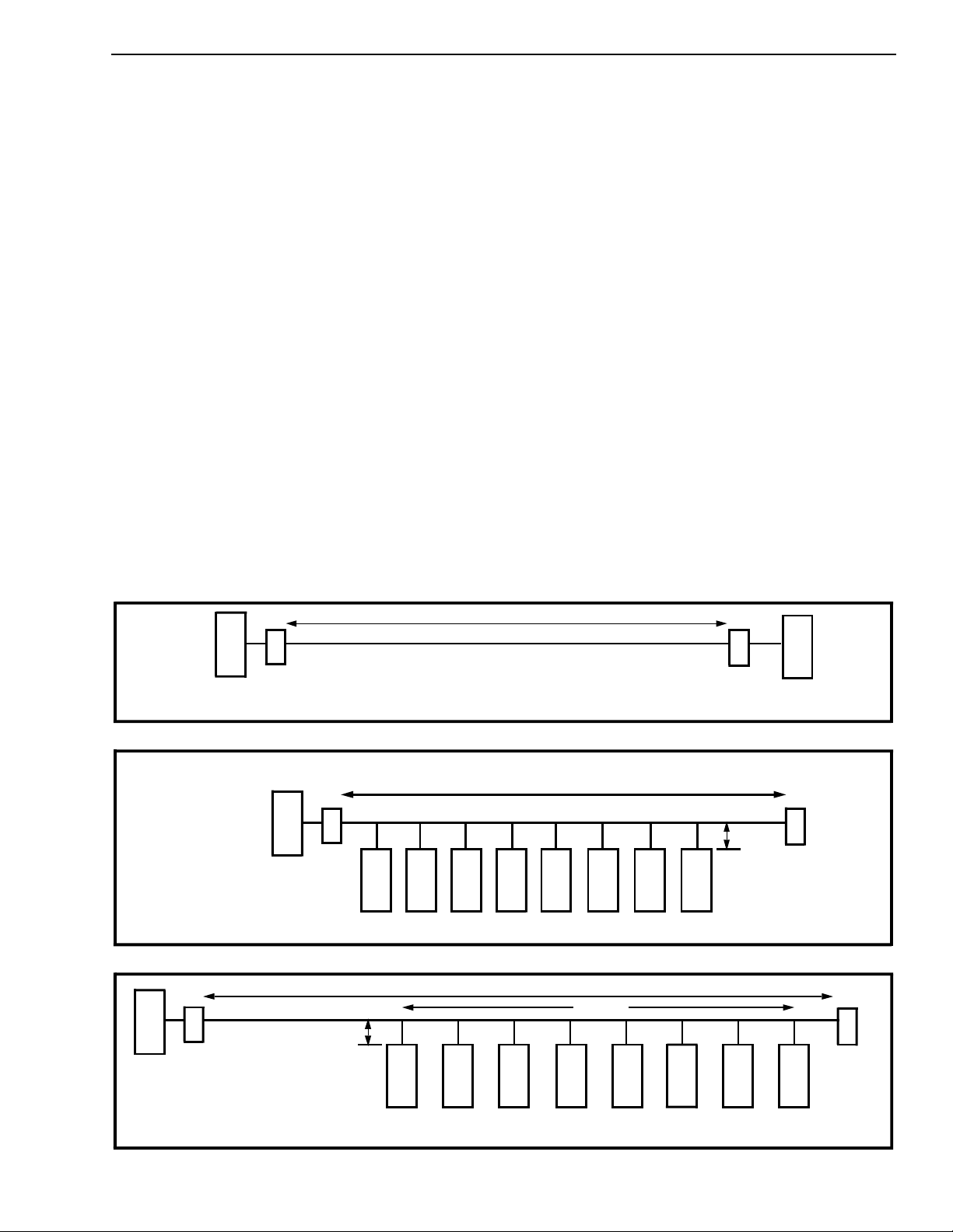
Figure 9 - Short Passive Bus Configuration, up to 8 TEs can be supported
NT
T
R
0 - 10 m
0 - 1 Km
Figure 8 - Poin t-to-Po int Confi guratio n
100 m for 75 Ω impedance cable and 200 m for 150 Ω impedance cable
TE
TE TE TE TE TE TE TE
100 - 200 m
0-500 m
0-50 m
T
R
0 - 10 m
TE
T
R
T
R
NT is operating in adaptive timing
TR is the line termination resistor = 100 Ω
Figure 10 - Extended Passive Bus Configuration, up to 8 TEs can be supported
TE TE TE TE TE TE TE
TE
9-81
MT8931C Preliminary Information
After successfully completing a transmission, the
internal priority level is reduced from high to low.
The internal priority will only be increased once the
terminal count for the respective level of priority has
been achieved. (e.g., if TE has high priority
internally and externally, it must count 8 consecutive
ones in the D-echo channel. Once this is achieved
and successful transmission has been completed,
the internal priority is reduced to a lower level (i.e.,
count = 9). This terminal will not return to the high
internal priority until 9 consecutive ones have been
monitored on the D-echo channel).
Line Wiring Configuration
The MT8931C can interface to any of the three
wiring configurations which are specified by the
CCITT Recommendation I.430 and ANSI T1.605
(refer to Figures 8 to 10). These consist of a
point-to-point or one of the two point-to- multipoint
configurations (i.e., short passive bus or the
extended passive bus). The selection of line
configurations is performed using the timing bit (B4
of NT Mode Control Register).
For the short passive bus, TE devices are connected
at random points along the cable. However, for the
extended passive bus all connection points are
grouped at the far end of the cable from the NT.
For an NT SNIC in fixed timing mode, the VCO and
Rx filters/peak detectors are disabled and the
threshold voltage is fixed. However, for a TE SNIC
or an NT SNIC (in adaptive timing mode), the VCO
and Rx filters/peak detectors are enabled. In this
manner, the device can compensate for variable
round trip delays and line attenuation using a
threshold voltage set to a fixed percentage of the
pulse peak amplitude.
Another operation can be implemented using the
SNIC in the star configuration as shown in Figure 14.
This mode allows multiple NTs, with physically
independent S-Busses, to share a common input
source and transfer information down the S-Bus to
all TEs . All NT devices connected into the star will
receive the information transmitted by all TEs on all
branches of the star, exactly as if they were on the
same physical S-Bus. All NTs in the star
configuration must be operating in fixed timing mode.
Refer to the description of the star configuration in
the ST-BUS section.
The SNIC has one last mode of operation called the
NT slave mode. This has the effect of operating the
SNIC in network termination mode (XTAL1/NT pin =
1) but having the frame structure and registers
description defined by the TE mode. This can be
used where multiple subscriber loops must carry a
fixed phase relation between each line. A typical
F0b
C4b
ST-BUS
BIT CELLS
Channel0Channel
1
Channel 31
Bit 0
125 µs
Channel
2
Bit 7 Bit 6 Bit 5 Bit 4 Bit 3 Bit 2 Bit 1 Bit 0
•••
(8/2048) ms
Channel30Channel31Channel
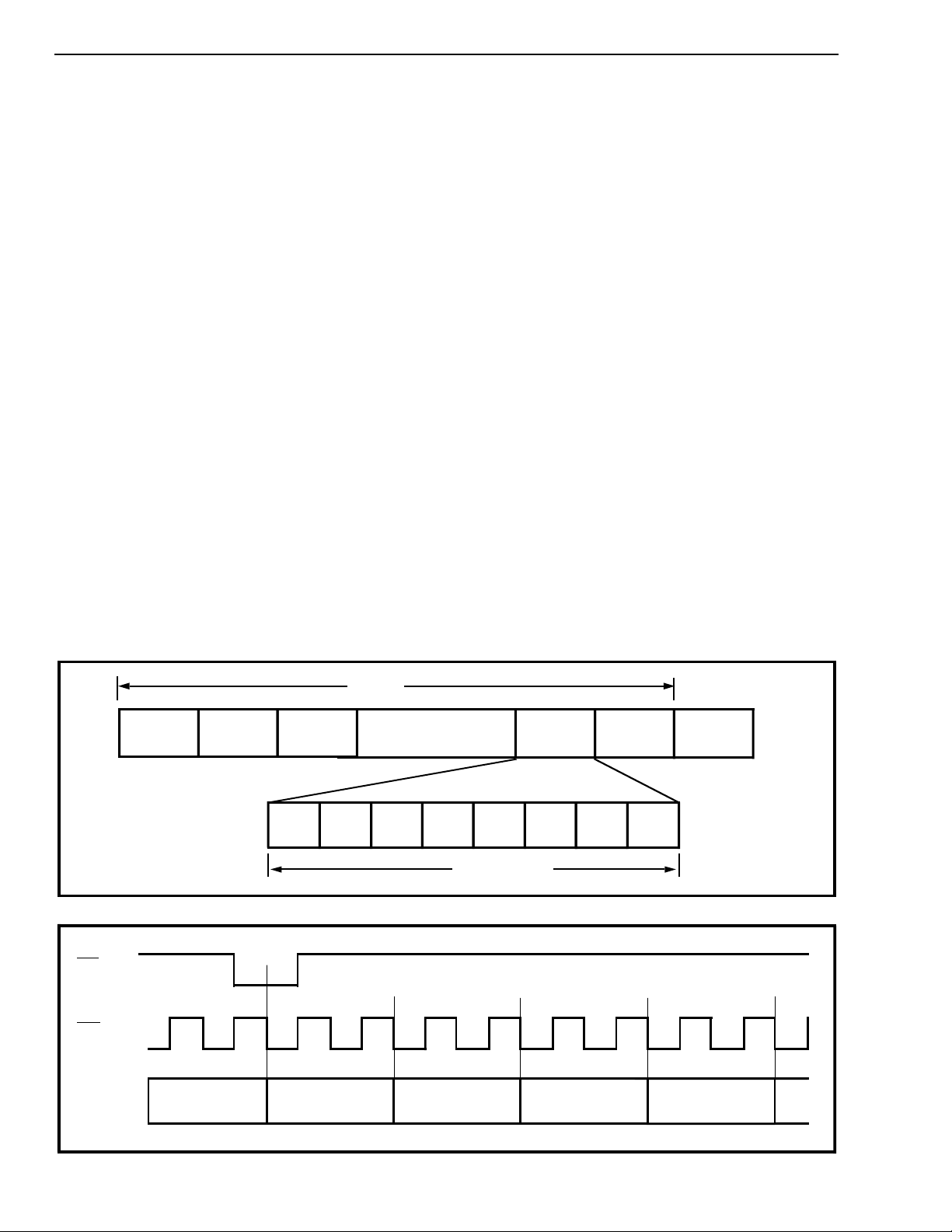
Figure 11 - ST-BUS Stream Format
Channel 0
Bit 7
Channel 0
Bit 6
Channel 0
Bit 5
0
Channel 0
Bit 4
9-82
Figure 12 - Cloc k & Fram e Alignm ent for ST-BUS Stream s
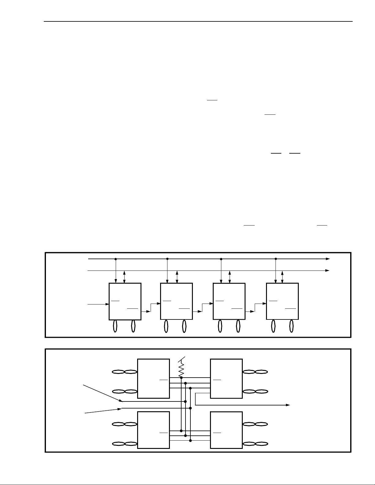
Preliminary Information MT8931C
situation is when the system is trying to synchronize
two nodes of a synchronous network. This allows
multiple TEs to share a common ST-BUS timebase.
The synchronization of the loops is established by
using the clock signals produced by a local TE as an
input timi ng source to the N T s l ave .
Adaptive Tim in g Operation
On power-up or after a reset, the SNIC in NT mode is
set to operate in fixed timing. To switch to adaptive
timing, the user should:
1) set the DR b it to 1
2) set the Timing bit to 1 in the C-channel
Control Register
3) wait for 100 ms period
4) proceed in using the AR and DR bits as
desired
Switching from adaptive timing mode is completed
by resetting the Timing bit.
ST-BUS Interface
The ST-BUS is a synchronous time division
multiplexed serial bussing scheme with data streams
operating at 2048 kbit/s configured as 32, 64 kbit/s
channels (refer to Fig. 11). Synchroni-zation of the
data transfer is provided from a frame pulse which
identifies the frame boundaries and repeats at an 8
kHz rate. Figure 4 shows how the frame pulse
(F0b
) defines the ST-BUS frame boundaries. All
data is clocked into the device on the rising edge of
the 4096 kHz clock (C4b
into the bit cell, while data is clocked out on the
falling edge of the 4096 kHz clock at the start of the
bit cell.
All timing signals (i.e. F0b
bidirectional (denoted by the terminating b). The
I/O configuration of these pins is controlled by the
mode of operation (NT or TE). In the NT mode, all
synchronized signals are supplied from an external
source and the SNIC uses this timing while
transferring info rmat ion to and from th e S or
ST-BUS. In the TE mode, an on-board analog
phase-locked loop extracts timing from the received
data on the S-Bus and generates the system
4096 kHz (C4b
) and frame pulse (F0b). The
analog phase-locked loop also maintains proper
phase relation between the timing signals as well as
) three quarters of the way
& C4b) are identified as
ST-BUS Clock
ST-BUS
Stream
System
Frame Pulse
System
Frame Pulse
Input
ST-BUS Stream
Active on
Channel 0 - 3
MT8931C
NT
F0b
F0od
to TE to TE to TE to TE
MT8931C
F0b
Active on
Channels 4 - 7
NT
F0od
MT8931C
NT
F0b
Active on
Channels 8 - 11
F0od
Figure 13 - Daisy Chaining the SNIC
V
DD
to TE
to TE
MT8931C
NT
STAR
F0b
DSTi
MT8931C
NT
STAR
F0b
DSTi
MT8931C
NT
STAR
F0b
DSTi
DSTo
MT8931C
NT
STAR
F0b
DSTi
to TE
to TE
MT8931C
NT
F0b
Active on
Channels 12 - 15
F0od
Output
ST-BUS Stream
Figure 14 - NT in Star Configuration
9-83
 Loading...