MITEL MT8930CE, MT8930CP Datasheet
CMOS ST-BUS FAMILY
MT8930C
Subscriber Network Interface Circuit
Features
• ETS 300-012, CCITT I.430 and ANSI T1.605
S/T interface
• Full-duplex 2B+D, 192 kbit/s transmission
• Link activation/deactivation
• D-channel access contention resolution
• Point-to-point, point-to-multipoint and star
configurations
• Master (NT)/Slave (TE) modes of operation
• Exceeds loop length requirements
• Complete loopback testing capabilities
• On chip HDLC D-channel protocoller
• 8 bit Motorola/Intel microprocessor interface
• Controllerless or microprocessor-controlled
operation
• Mitel ST-BUS interface
• Low power CMOS technology
• Single 5 volt power supply
Applications
• ISDN NT1
• ISDN S or T interface
• ISDN Terminal Adaptor (TA)
• Digital sets (TE1) - 4 wire ISDN interface
• Digital PABXs, Digital Line Cards (NT2)
ISSUE3 November 1997
Ordering Information
MT8930CE 28 Pin Plastic DIP
MT8930CP 44 Pin PLCC
-40°C to +85°C
Description
The MT8930C Subscriber Network Interface Circuit
(SNIC) implements the ETSI ETS 300-012, CCITT
I.430 and ANSI T1.605 Recommendations for the
ISDN S and T reference points. Providing point-topoint and point-to-multipoint digital transmission, the
SNIC may be used at either end of the subscriber
line (NT or TE).
An HDLC D-channel protocoller is included and
controlled through a Motorola/Intel microprocessor
port. A controllerless mode allows the SNIC to
operate without a microprocessor.
The MT8930C is fabricated in Mitel’s CMOS process.
DSTi
DSTo
F0od
C4b
F0b
STAR/Rsto
CK/NT
Cmode
ST-BUS
Interface
Timing
and
Control
Rsti HALF AD0-7 R/W/WR,
D-channel Priority
Mechanism
PLL
AFT/PRI
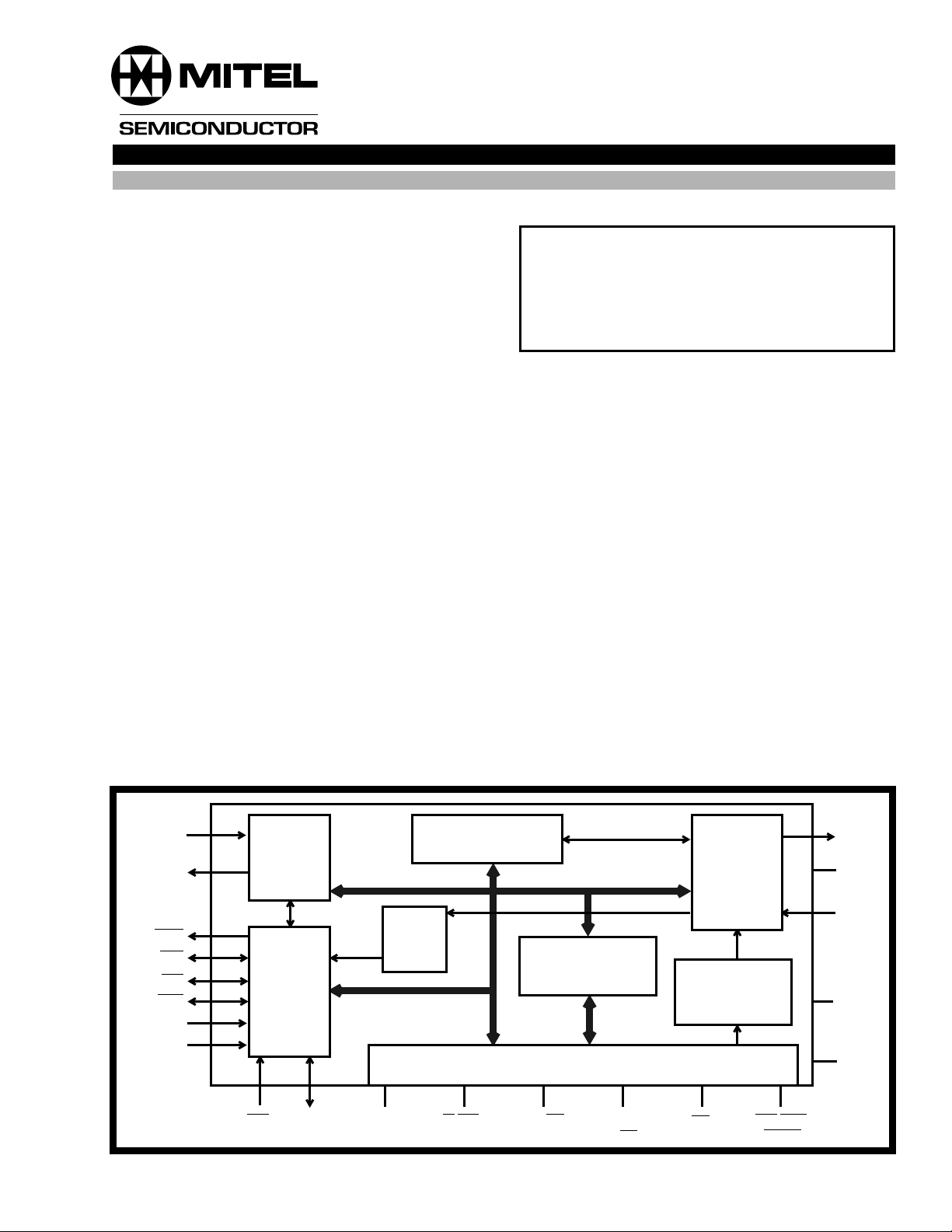
Figure 1 - Functional Block Diagram
HDLC
Transceiver
Microprocessor Interface
DS/RD,
DinB
AS/ALE,
SC
P/
CS,
DReq
S-Bus
Link
Interface
Link
Activation
Controller
IRQ/NDA,
DCack
LTx
VBias
LRx
V
DD
V
SS
9-33
MT8930C
HALF
F0od
DSTi
DSTo
Cmode
W/WR, AFT/PRI
R/
IRQ/NDA, DCack
CK/NT
RD, DinB
DS/
AS/ALE, P/SC
CS, DReq
C4b
F0b
VSS
1
2
3
4
5
6
7
8
9
10
11
12
13
14
28 PIN PDIP
28
VDD
27
VBias
26
LTx
25
LRx
24
STAR/
23
Rsti
22
AD7, DR
21
AD6, AR
20
AD5, M/S
19
AD4, MCH
18
AD3, MFR
17
AD2, SYNC/BA
16
AD1, IS1
15
AD0, IS0
Rsto
Cmode
CK/NT
R/
W/WR, AFT/PRI
RD, DinB
DS/
F0od
DSTi
DSTo
NC
NC
NC
NC
NCNCC4b
F0b
65432 44434241
7
8
9
10
11
12
13
14
15
16
17
NC
CS, DReq
AS/ALE, P/SC
NC
HALF
VDD
1
231819202122 2425262728
NC
VSS
AD0, IS0
IRQ/NDA, DCack
44 PIN PLCC
VBias
LRx
LTx
NC
40
39
38
37
36
35
34
33
32
31
30
29
NC
NC
AD1, IS1
AD2, SYNC/BA
NC
STAR/
Rsto
Rsti
NC
AD7, DR
AD6, AR
NC
AD5, M/S
AD4, MCH
AD3, MFR
NC
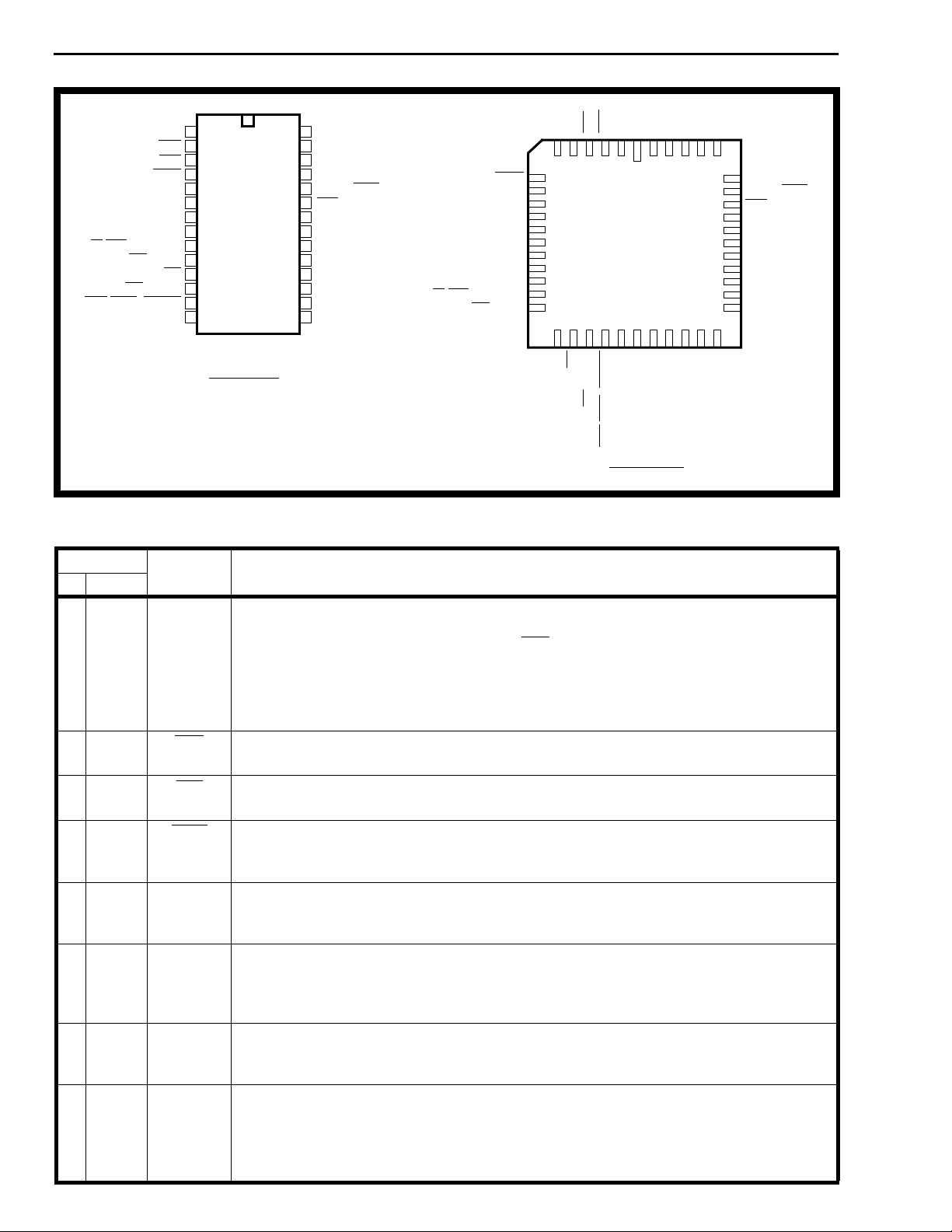
Figure 2 - Pin Connections
Pin Description
Pin #
DIP PLCC
1 2 HALF HALF Input/Output: this is an input in NT mode and an output in TE mode identifying
23 C4b 4.096 MHz Clock: a 4.096 MHz ST-BUS Data Clock input in NT mode.
34 F0b Frame Pulse: an active low frame pulse input indicating the beginning of active ST-
47 F0od Delayed Frame Pulse Output: an active low delayed frame pulse output indicating
5 8 DSTi Data ST-BUS Input: a 2048 kbit/s serial PCM/data ST-BUS input with D, C, B1, and B2
6 9 DSTo Data ST-BUS Output: a 2048 kbit/s serial PCM/data ST-BUS output with D, C, B1 and
7 13 Cmode Controller Mode Select Input: when high, microprocessor control is selected. When
8 14 CK/NT TE Clock/Network Termination Mode Select Input. For TE mode, this pin must be
Name Description
which half of the S-interface frame is currently being written/read over the ST-BUS
(HALF = 0 sampled on the falling edge of C4b within the frame pulse low window,
identifies the information to be transmitted/received in the first half of the S-Bus frame
while HALF = 1 identifies the information to be transmitted/received into the second half
of the S-Bus frame). Tying this pin to VSS or VDDin NT mode will allow the device to
free run. This signal can also be accessed from the ST-BUS C-channel.
In TE mode, a 4.096 MHz output clock phase-locked to the line data signal.
BUS channel times in NT mode. Frame pulse output in TE mode.
the end of active ST-BUS channels for this device. Can be used to daisy chain
to other ST-BUS devices to share an ST-BUS stream.
channels assigned to the first four timeslots. These channels contain data to be
transmitted on the line and chip control information.
B2 channels assigned to the first four timeslots respectively. The remaining timeslots
are placed into high impedance. These channels contain data received from the line
and chip status information.
low the controllerless mode is enabled and the microport pins are redefined as control
inputs and status outputs.
tied to VSS or to a 4.096 MHz clock (a clock is required for standard ISDN TE
applications). For NT mode, this pin must be tied to VDD. Refer to “ST-BUS Interface”
section for further explanation. A pull-up resistor is needed when driven by a TTL
device.
9-34

Pin Description (continued)
Pin #
DIP PLCC
916R/W/WR
10 17 DS/RD
11 19 AS/ALE
12 20 CS
13 21 IRQ
14 22 V
15-2224-26
30-32
34-35
15-1624-
25
Name Description
Read/Write or Write Input (Cmode = 1): defines the data bus transfer as a read (R/
W=1) or a write (R/W=0) in Motorola bus mode. Redefined to WR in Intel bus mode.
AFT/PRI
Adaptive-Fixed Timing/Priority Select Input (Cmode=0): in NT mode, causes the
PLL and Rx filters and peak detectors to be disabled in favour of fixed timing and fixed
thresholds for short passive bus operation (0=fix ed, 1=adaptiv e). In TE mode , this is the
Priority input. High priority (PRI=1) is normally reserved for signalling.
Data Strobe/Read Input (Cmode = 1): active high input indicates to the SNIC that
valid data is on the bus during a write operation or that the SNIC must output data
during a read operation in Motorola bus mode. Redefined to RD in Intel bus mode.
DinB
D-Channel in B1 Timeslot Input (Cmode = 0): active high input that causes all
eight ST-BUS D-channel bits, instead of the usual two bits, to be routed to and
from the S-interface B1 timeslot. When active, marks are transmitted in the
S-interface D-channel.
Address Strobe/Address Latch Enable Input (Cmode = 1): in Motorola bus mode
the falling edge is used to strobe the address into the SNIC during microprocessor
access. Redefined to ALE in Intel bus mode.
P/SC
Parallel/Serial Control Input (Cmode = 0): determines if the serial C-channel
(P/SC=0) or microport pins (P/SC=1) are the source of chip control when controllerless
mode is selected. If the ST-BUS is chosen as the source, the dedicated Control input
pins are ignored but the status output pins remain valid.
Chip Select Input (Cmode=1): active low input used to select the SNIC for
microprocessor access.
DReq
D-Channel Request Input (Cmode = 0): an active high input that in TE mode only
causes the SNIC to transmit a “01111110” flag immediately if the D-channel is free, or
wait until it becomes available and then transmit the flag. The DCack signals the
successful acquisition of the D-channel. If DReq is tied low, continuous ones are
transmitted in the S-Bus D-channel.
IC
Internal Connection (Cmode = 0): tie to VSS for normal operation in NT mode only.
Interrupt Request (Open Drain Output) (Cmode = 1): an output indicating an
unmasked HDLC interrupt. The interrupt remains active until the microprocessor clears
it by reading the HDLC Interrupt Status Register. This interrupt source is enabled with
B2=0 of Master Control Register.
NDA
New Data Available (Open Drain Output) (Cmode = 1): an active low output signal
indicating availability of new data from the S-Bus. This signal is selected with B2=1 of
Master Control Register.
DCack
D-Channel Acknowledge (Open Drain Output) (Cmode = 0): in TE mode only
indicates that the SNIC has gained access to the D-channel in response to a DReq and
has transmitted the first zero of an opening flag. The user should immediately begin
transmitting the rest of the packet over the ST-BUS D-channel. If this signal goes high
in the middle of transmission, the TE has lost the bus and must regain access of the Dchannel before retransmitting the packet.
IC
Internal Connection (Open Drain Output) (C-mode=0). This pin is not used in NT
mode and should be left disconnected.
This pin must be tied to VDD with a 10kΩ resistor.
SS
Ground.
AD0-7 Bidirectional Address/Data Bus (Cmode = 1): electrically and logically compatible to
either Intel or Motorola micro-bus specifications. If DS/RD is low on the rising edge of
AS/ALE then the chip operates to Motorola specs. If DS/RD is high on the rising edge
of AS/ALE Intel mode is selected. Taking Rsti low sets Motorola mode.
IS0-IS1 Internal State Outputs (Cmode =0): Binary encoded state number outputs.
IS0 IS1 NT Mode TE Mode
0 0 deactivated deactivated
0 1 pending deactivation synchronized
1 0 pending activation activation request
1 1 activated activated
MT8930C
9-35

MT8930C
Pin Description (continued)
Pin #
DIP PLCC
17 26 SYNC/BA Synchronization/Bus Activity Output (Cmode = 0): output indicating synchronization
18 30 MFR Multiframe Input/Output (Cmode=0): multiframe input in NT mode or output in TE
19 31 MCH Maintenance Channel (Q-channel) Input/Output (Cmode=0): an output in NT mode
20 32 M/S M/S Input/Output (Cmode=0): M/S bit input in NT mode or M/S bit output in TE mode.
21 34 AR Activate Request Input (Cmode = 0): asserting AR with DR = 0 will initiate the
22 35 DR Deactivate Request Input (Cmode = 0): asserting DR high will initiate the appropriate
23 37 Rsti Reset Input: Schmitt trigger reset input. If ’0’, sets all control registers to the default
24 38 STAR/Rsto Star/Reset (Open Drain Output): 192kbit/s Rx data output fixed relative to the ST-
25 40 LRx Receive Line Signal Input: this is a high impedance input for the pseudoternary line
26 42 LTx Transmit Line Signal Output: this is a current source output designed to drive a
27 43 V
28 44 V
1,5-6,10-
12,15,18,
23,27-
29, 33,
36, 39, 41
Name Description
to incoming RX frames when activation request is asserted and the deactivation request
is ’0’ (AR = 1 and DR = 0). Synchronization is declared once three successive frames
conforming to the 14-bit bipolar violation criteria have been detected. If part is
deactivated or activation request is ’0’ (AR = 0 or DR = 1), this pin indicates the
presence of bus activity.
mode. Setting this pin to one in NT mode when HALF = 1, forces the FA, N pair to 1, 0
respectively. This pin going high in TE mode indicates that FA= 1 & N= 0 has been
received. This signal is updated on the rising edge of the HALF signal.
which is valid only in the frame following the transmission of MFR. In TE mode, this is
the maintenance channel (Q-channel) input which is transmitted in the FA and L bits
following the reception of the multiframe signal. This input is sampled on the falling
edge of the HALF signal.
M is read or written when HALF=1 while S is read or written when HALF=0.
appropriate S-interface activation sequence coded in the NT or TE activation/
deactivation controller.
S-interface deactivation sequence coded in the NT or TE activation/ deactivation
controller.
conditions, resets activation state machines to the deactivated state, resets HDLC,
clears the HDLC FIFO‘s. Sets the microport to Motorola bus mode.
BUS timebase. A group of NTs, in fixed timing mode, can be wire or’ed together to
create a Star configuration. Active low reset output in TE mode indicating 128
consecutive marks have been received. Can be connected directly to Rsti to allow NT
to reset all TEs on the bus. This pin must be tied to VDDwith a 10 kΩ resistor.
signal to be connected to the line through a 2:1 ratio transformer. See Figures 20 and
21. A DC bias level on this input equal to V
must be maintained.
Bias
nominal 50 ohm line through a 2:1 ratio transformer. See Figures 20 and 21.
Bias
Bias Voltage: analog ground for Tx and Rx transformers. This pin must be decoupled
to VDD through a 10µF capacitor with good high frequency characteristics (i.e.,
tantalum).
DD
Power Supply Input.
NC No Connection.
9-36
MT8930C
Functional Description
The MT8930C Subscriber Network Interface Circuit
(SNIC) is a multifunction transceiver providing a
complete interface to the S/T Reference Point as
specified in ETS 300-012, CCITT Recommendation
I.430 and ANSI T1.605. Implementing both
point-to-point and point-to-multipoint voice/data
transmission, the SNIC may be used at either end of
the digital subscriber loop. A programmable digital
interface allows the MT8930C to be configured as a
Network Termination (NT) or as a Terminal
Equipment (TE) device.
The SNIC supports 192 kbit/s (2B+D + overhead) full
duplex data transmission on a 4-wire balanced
transmission line. Transmission capability for both B
and D channels, as well as related timing and
synchronization functions, are provided on chip. The
signalling capability and procedures necessary to
enable customer terminals (TEs) to be activated and
deactivated, form part of the MT8930C’s
functionality. The SNIC handles D-channel resource
allocation and prioritization for access contention
resolution and signalling requirements in passive bus
line configurations. Control and status information
allows implementation of maintenance functions and
monitoring of the device and the subscriber loop.
An HDLC transceiver is included on the SNIC for link
access protocol handling via the D-channel.
Depacketized data is passed to and from the
transceiver via the microprocessor port. Two 19 byte
deep FIFOs, one for transmit and one for receive, are
provided to buffer the data. The HDLC block can be
set up to transmit or receive to/from either the
S-interface port or the ST-BUS port. Further, the
transmit destination and receive source can be
independently selected, e.g., transmit to S-interface
while receiving from ST-BUS. The transmit and
receive paths can be separately enabled or disabled.
Both, one and two byte address recognition is
supported by the SNIC. A transparent mode allows
data to be passed directly to the D channel without
being packetized.
A block diagram of the MT8930C is shown in Figure
1. The SNIC has three interface ports: a 4-wire
CCITT compatible S/T interface (subscriber loop
interface), a 2048 kbit/s ST-BUS serial port, and a
general purpose parallel microprocessor port. This
8-bit parallel port is compatible with both Motorola or
HALF
C4bi
F0bi
F0od
DSTi
DSTo
Cmode
NT
W/WR
R/
RD
DS/
AS/ALE
CS
IRQ, NDA
VSS
HALF
C4bi
F0bi
F0od
DSTi
DSTo
Cmode
NT
AFT
DinB
SC
P/
VSS
NT MODE
1
2
3
4
5
6
7
8
9
10
11
12
13
14
NT MODE
1
2
3
4
5
6
7
8
9
10
11
IC
12
IC
13
14
28
27
26
25
24
23
22
21
20
19
18
17
16
15
28
27
26
25
24
23
22
21
20
19
18
17
16
15
VDD
VBias
LTx
LRx
STAR
Rsti
AD7
AD6
AD5
AD4
AD3
AD2
AD1
AD0
VDD
VBias
LTx
LRx
STAR
Rsti
DR
AR
M/Si
MCHo
MFRi
SYNC/BA
IS1
IS0
CONTROLLER MODE
Cmode
W/WR
R/
DS/
AS/ALE
IRQ, NDA
CONTROLLERLESS MODE
Cmode
DCack
HALF
C4bo
F0bo
F0od
DSTi
DSTo
CK
RD
CS
VSS
HALF
C4bo
F0bo
F0od
DSTi
DSTo
CK
PRI
DinB
SC
P/
DReq
VSS
TE MODE
1
2
3
4
5
6
7
8
9
10
11
12
13
14
TE MODE
1
2
3
4
5
6
7
8
9
10
11
12
13
14
28
27
26
25
24
23
22
21
20
19
18
17
16
15
28
27
26
25
24
23
22
21
20
19
18
17
16
15
VDD
VBias
LTx
LRx
Rsto
Rsti
AD7
AD6
AD5
AD4
AD3
AD2
AD1
AD0
VDD
VBias
LTx
LRx
Rsto
Rsti
DR
AR
M/So
MCHi
MFRo
SYNC/BA
IS1
IS0
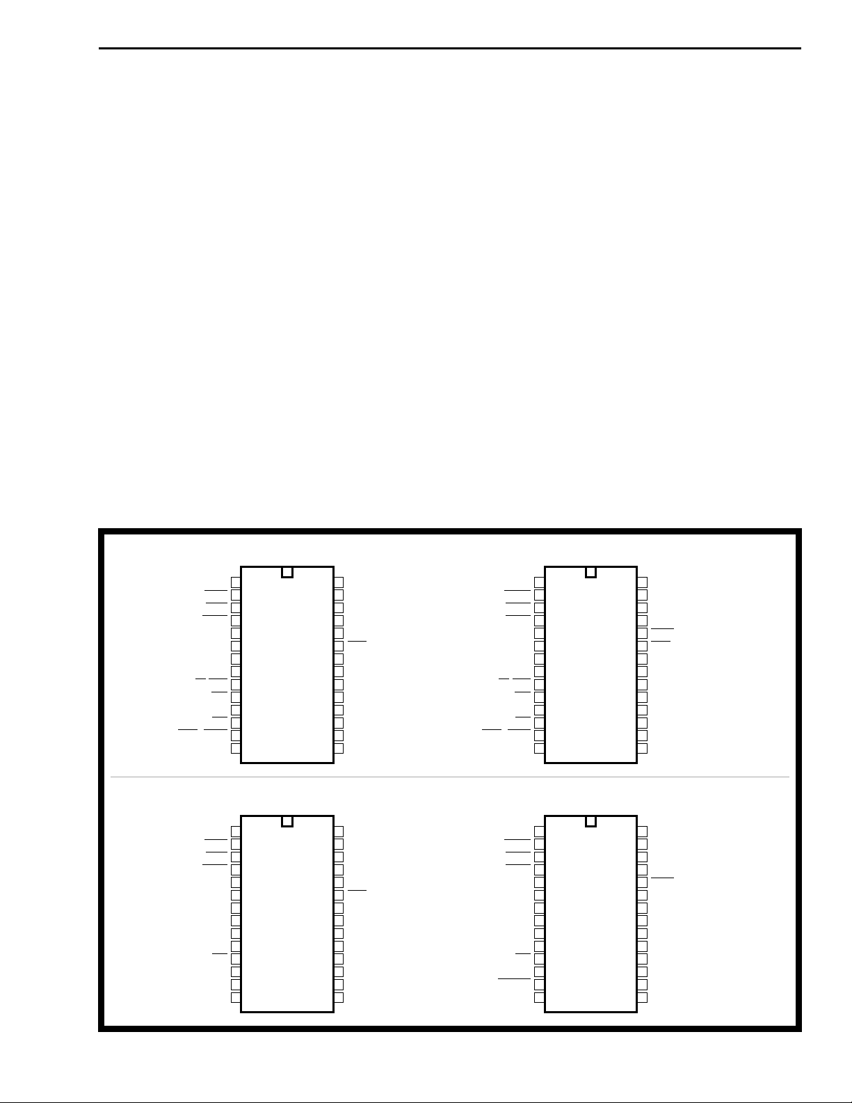
Figure 3 - SNIC Pin Connections in Various Modes
9-37
MT8930C
Intel microprocessor bus signals and timing. The
SNIC also has provisions for a controllerless mode
(Cmode=0), where the microprocessor port is
redefined to allow access to the control/status
registers via external hardware.
The three major blocks of the MT8930C, consisting
of the system serial interface (ST-BUS), HDLC
transceiver, and the digital subscriber loop interface
(S-interface) are interconnected by high speed data
busses. Data sent to and received from the
S-interface port (B1, B2 and D channels) can be
accessed from either the parallel microprocessor
port or the serial ST-BUS por t. This is also true for
SNIC control and status information (C-channel).
Depacketized D-channel information to and from the
HDLC section can only be accessed through the
parallel microprocessor port.
S-Bus Interface
B1 B1 B1 B1 B1 B1 B1 B1 B2 B2 B2 B2 B2 B2 B2 B2
C7 C6 C5 C4 C3 C2 C1 C0
B1 B1 B1 B1 B1 B1 B1 B1 B2 B2 B2 B2 B2 B2 B2 B2
C7 C6 C5 C4 C3 C2 C1 C0
The S-Bus is a four wire, full duplex, time division
multiplexed transmission facility which exchanges
information at 192 kbit/s rate including two 64 kbit/s
PCM voice or data channels, a 16 kbit/s signalling
channel and 48 kbit/s for synchronization and
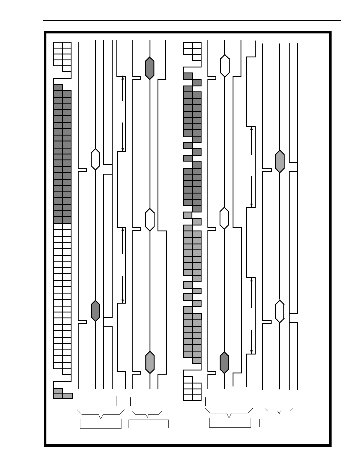
overhead. The relative position of these channels
with respect to the ST-BUS is shown in Figures 4
and 5.
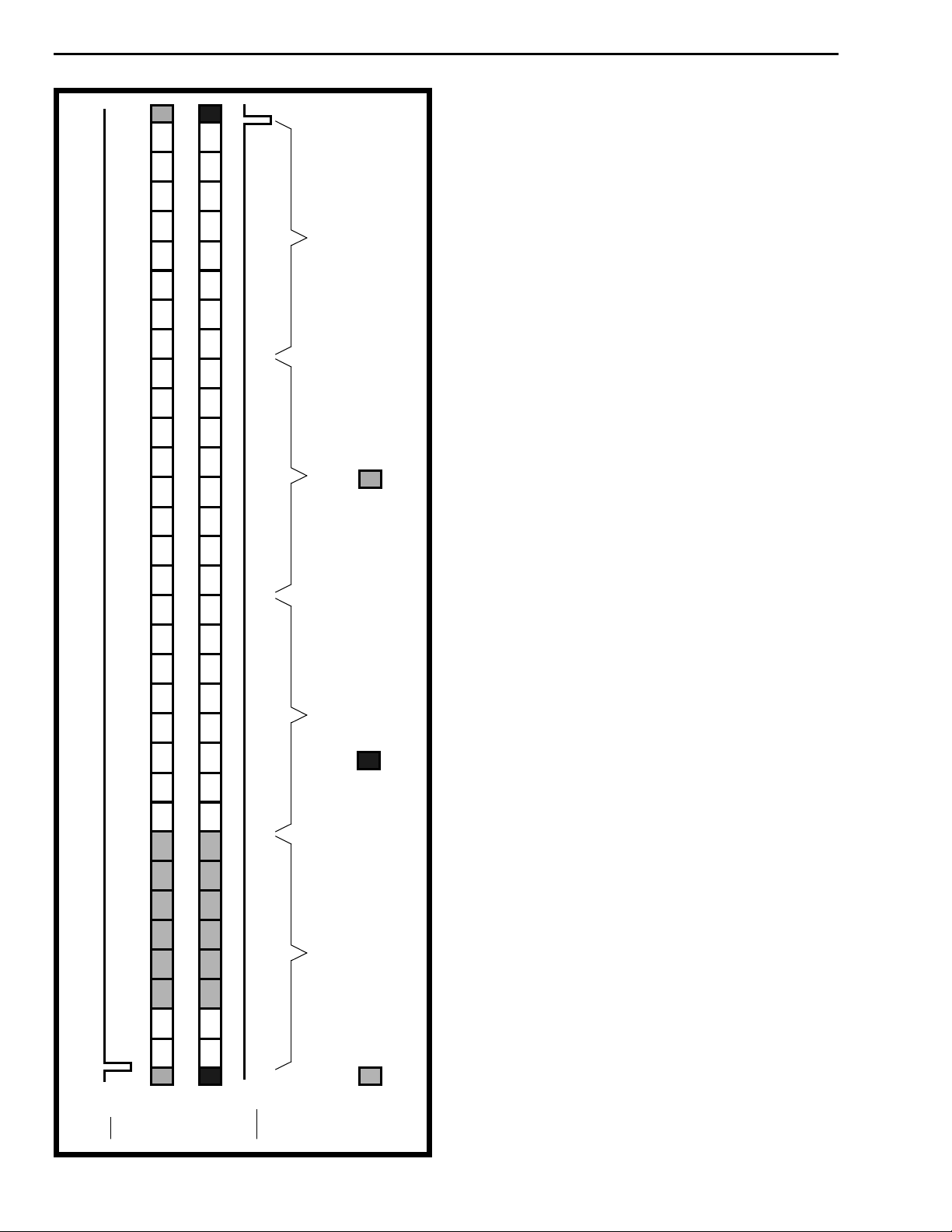
The SNIC makes use of the first four channels on the
ST-BUS to transmit and receive control/status and
data to and from the S-interface port. These are the
B, D and C-channels (see Figure 4).
Channel 1 (C) Channel 2 (B1) Channel 3 (B2)Channel 0 (D)
The B1 and B2 channels each have a bandwidth of
64 kbit/s and are used to carry PCM voice or data
across the network.
The D-channel is primarily intended to carry
signalling information for circuit s witching through the
ISDN network. The SNIC provides the capability of
having a 16 kbit/s or full 64 kbit/s D-channel by
allocating the B1-channel timeslot to the D-channel.
Access to the depacketized D-channel is only
granted through the parallel microprocessor port.
F0b
D0 D1 D2 D3 D4 D5 D6 D7
DSTi
D0 D1 D2 D3 D4 D5 D6 D7
DSTo
F0od
Figure 4 - ST-BUS Channel Assignment
9-38
Only valid with 64 kbit/s D-channel Output in high impedance state Don’t care
The C-channel provides a means for the system to
control and monitor the functionality of the SNIC.
This control/status channel is accessed by the
system through the ST-BUS or microprocessor
port. The C-channel provides access to two
registers which provide complete control over the
state activation machine, the D-channel priority
mechanism as well as the various maintenance
functions. A detailed description of these registers is
discussed in the microprocessor port interface.
MT8930C
B1 B1B1
62.5 µs
Note: Shaded areas reveal data mapping
B1
B1 B1 B1B1 B1B1 EB1 D0 B2 B2 B2 B2 B2 B2 B2 B2 ES D1 L F L B1 B1FL B1B1 B1B1 B1B1 B1 E D0 A Fa N B2 B2 B2 B2B1 B2 B2 B2 B2 E D1 M B1 B1 B1
B2 L LD1 B1B1 B1B1 B1 B1 B1 L D0 L B2 B2 B2 B2B1 B2 B2 B2 B2 L D1 LB2 L LD1 LFB1B1 B1 B1 B1 B1 B1 L D0 L Fa LB1 B2 B2 B2 B2 B2 B2 B2 FL
62.5 µs
62.5 µs
A = Activation bit
M = Multiframing bit
S = S-channel bit
62.5 µs
Figure 5 - S-Bus Frame Structure and Functional Timing
NT to TE
F0b
DSTi
NTX
Input
HALF
M
Fa & N (NT to TE) = Auxiliary framing bits
Fa (TE to NT) = Auxiliary framing bit or Q-channel bit
B1 = Bit within B1-channel
B2 = Bit within B2-channel
F0b
DSTi
HALF
NDA
F0b
DSTo
HALF
NDA
F0b
DSTo
HALF
Output
T
TER
C
V
TE to NT
TEX
Output
M
T
NTR
Input
V
C
F = Framing bit
L = DC balancing bit
D = Bit within D-channel
E = D-echo channel bit
9-39
MT8930C
Line Code
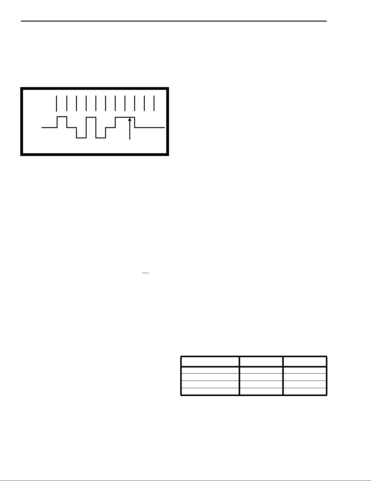
The line code used on the S-interface is a Pseudo
ternary code with 100% pulse width as seen in
Figure 6 below. Binary zeros are represented as
marks on the line and successive marks will
alternate in polarity.
BINARY
VALUE
LINE
SIGNAL
0100010011
Violation
Figure 6 - Alternate Zero Inversion Line Code
A mark which does not adhere to the alternating
polarity is known as a bipolar violation.
Framing
The valid frame structure transmitted by the NT and
TE contains the following (refer Fig. 5):
NT to TE:
- Framing bit (F)
- B1 and B2 channels (B1,B2)
- DC balancing bits (L)
- D-channel bits (D0, D1)
- Auxiliary framing and N bit (Fa, N), N=Fa
- Activation bit (A)
- D-echo channel bits (E)
- Multiframing bit (M)
- S-channel bit
TE to NT:
- Framing bit (F)
- B1 and B2 channels (B1, B2)
- DC balancing bits (L)
- D-channel bits (D0, D1)
- Auxiliary framing bit (Fa) or Q-channel bit
The framing mechanism on the S-interface makes
use of line code violations to identify frame
boundaries. The F-bit violates the alternating
line code sequence to allow for quick identification of
the frame boundaries. To secure the frame
alignment, the next mark following the frame
balancing bit (L) will also produce a line code
violation. If the data following the balancing bit is all
binary ones, the zero in the auxiliary framing bit (Fa)
or N-bit (for the direction NT to TE) will provide
successive violations to ensure that the 14 bit
criterion (13 bit criterion in the direction TE to NT)
specified in Recommendations I.430 and T1.605 is
satisfied. If the B1-channel is not all binary ones, the
first zero following the L-bit will violate the line code
sequence, thus allowing subsequent marks to
alternate without bipolar violations.
The Fa and N bits can also be used to identify a
multiframe structure (when this is done, the 14 bit
criterion may not be met). This multiframe structure
will make provisions for a low speed signalling
channel to be used in the TE to NT direction
(Q-channel). It will consist of a five frame multiframe
which can be identified by the binary inversion of the
Fa and N-bit on the first frame and consequently on
every fifth frame of the multiframe . Upon detection of
the multiframe signal, the TE will replace the next Fabit to be transmitted with the Q-bit.
The DC balancing bits (L) are used to remove any
DC content from the line. The balancing bit will be a
mark if the number of preceding marks up to the
previous balancing bit is odd. If the number of
marks is even, the L-bit will be a space.
The A-bit is used by the NT during line activation
procedures (refer to state activation diagrams). The
state of the A-bit will advise the TE if the NT has
achieved synchronization.
The E-bit is the D-echo channel. The NT will reflect
the binary value of the received D-channel into the
E-bits. This is used to establish the access
contention resolution in a point-to-multipoint
configuration. This is described in more detail in the
section of the D-channel priority mechanism.
The M-bit is a second level of multiframing which is
used for structuring the Q-bits. The frame with Mbit=1 identifies frame #1 in the twenty frame
multiframe. The Q-channel is then received as
shown in Table 1. All synchronization with the
multiframes must be performed externally.
FRAME # Q-Bit M-Bit
1Q11
6Q20
11 Q3 0
16 Q4 0
Table 1. Q-channel Allocation
Bit Order
When using the B-channels for PCM voice, the first
bit to be transmitted on the S-Bus should be the sign
bit. This complies with the existing telecom
standards which transmit PCM voice as most
significant bit first. However, if the B-channels are to
9-40

MT8930C
carry data, the bit ordering must be reversed to
comply with the existing datacom standards (i.e.,
least significant bit first).
These contradicting standards place a restriction on
all information input and output through the serial
and parallel ports. Information transferred through
the serial ports, will maintain the integrity of the bit
order. Data sent to either serial port from the parallel
port, will transmit the least significant bit first.
Therefore, a PCM byte input through the
microprocessor port must be reordered to have the
sign bit as the least significant bit.
When the microprocessor reads D, B1 or B2 channel
data of either ST-BUS or S-bus serial por t, the least
significant bit read is the first bit received on that
particular channel of either serial port.
The D-channel received on the serial ST-BUS por ts
must be ordered with the least significant bit first as
shown in Figure 4. This also applies to the
D-channel directed to the ST-BUS from the
microprocessor port.
The C-channel bit mapping from the parallel port to
the ST-BUS is organized such that the most
significant bit is transmitted or received first.
State Activation
The state activation controller activates or
deactivates the SNIC in response to line activity or
external command. The controller is completely
hardware driven and need not be initialized by the
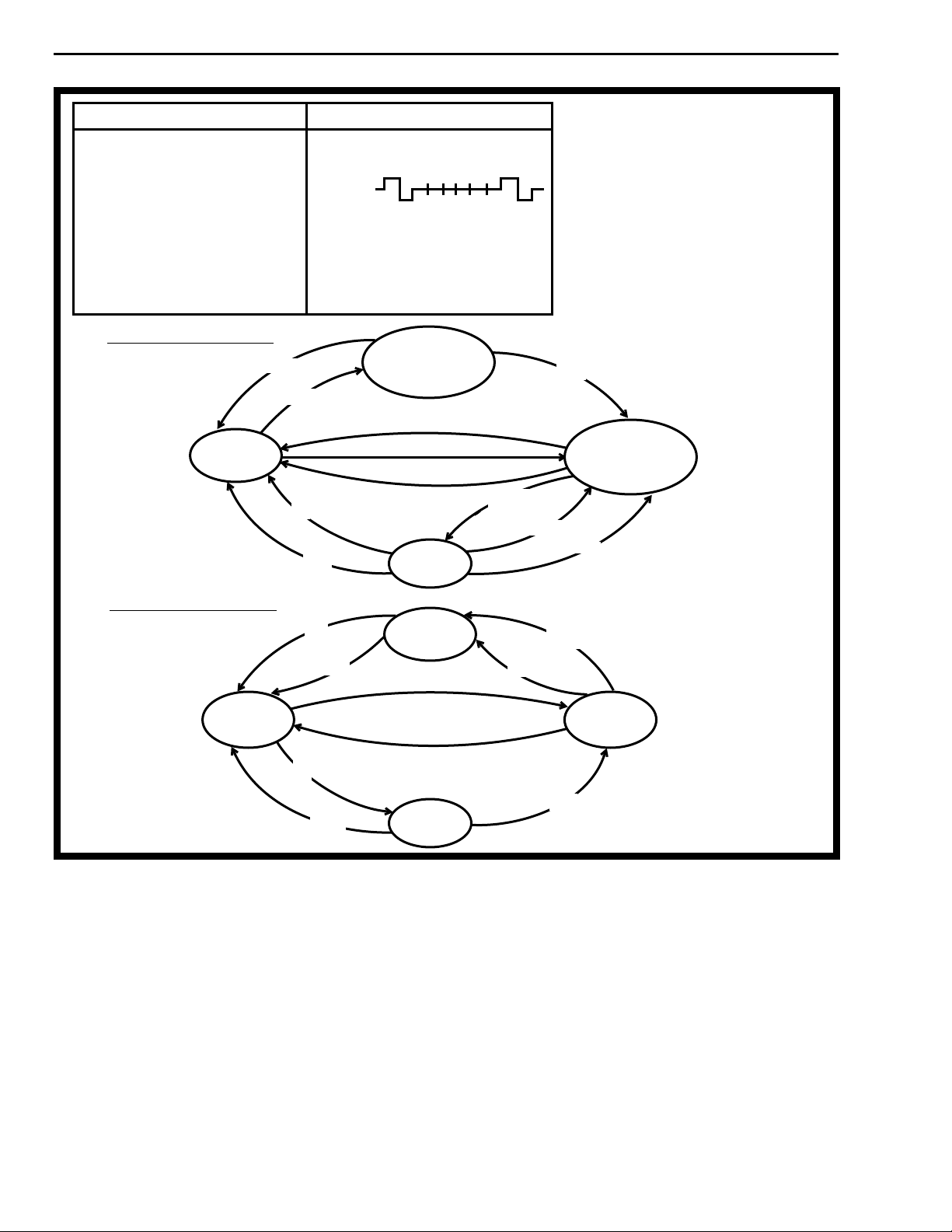
microprocessor. The state diagram for initialization
is shown in Figure 7.
The protocol used by the state activation controller is
defined as follows:
1) In the deactivated state, neither the NT nor
TE assert a signal on the line (Info0).
2) If the TE wants to initiate activation, it must
begin transmitting a continuous signal
consisting of a positive zero, a negative zero
followed by six ones (Info1).
3) Once the NT has detected Info1, it begins to
transmit Info2 which consists of an S-Bus
frame with zeros in the B and D-channel and
the activation bit (A-bit) set to zero.
4) As soon as the TE synchronizes to Info2, it
responds with a valid S-Bus frame with data
in the B1, B2 and D-channel (Info3).
5) The NT will then transmit a valid frame with
data in the B1, B2 and D-channel. It will also
set the activation bit (A) to binary one once
synchronization to Info3 is achieved.
If the NT wishes to initiate the activation, steps 2 and
3 are ignored and the NT starts sending Info2. To
initiate a deactivation, either end begins to send
Info0 (Idle line).
D-channel Priority Mechanism
The SNIC contains a hardware priority mechanism
for D-channel contention resolution. All TEs
connected in a point-to-multipoint configuration are
allocated the D-channel using a systematic
approach. Allocation of the D-channel is
accomplished by monitoring the D-echo channel
(E-bit) and incrementing the D-channel priority
counter with every consecutive one echoed back in
the E bit. Any zero found on the D-echo channel will
reset the priority counter.
There are two classes of priority within the SNIC,
one user accessible and the other being strictly
internal. The user accessible priority selects the
class of operation and has precedence over the
internal priority. The latter (internal priority), will
select the level of priority within each class (i.e., the
internal priority is a subsection of the user accessible
priority). User accessible priority selects the
terminal count as 8/9 or 10/11 consecutive ones on
the E-bit (8 being high priority while 10 being low
priority). The internal priority selects the terminal
between 8 or 9 for high class and 10 or 11 for low
class. The first terminal equipment to attain the E-bit
priority count will immediately take control of the
D-channel by sending the opening flag. If more than
one terminal has the same priority, all but one of
them will eventually detect a collision. The TEs that
detect a collision will immediately stop trans-mitting
on the D-channel, generate an interrupt through the
Dcoll bit, reset the DCack bit on the next frame
pulse, and restart the counting process. The
remainder of the packet in the Tx FIFO is ignored.
After successfully completing a transmission, the
internal priority level is reduced from high to low.
The internal priority will only be increased once the
terminal count for the respective level of priority has
been achieved (e.g., if TE has high priority inter nally
and externally, it must count 8 consecutive ones in
the D-echo channel. Once this is achieved and
successful transmission has been completed, the
internal priority is reduced to a lower level (i.e., count
= 9). This terminal will not return to the high inter nal
priority until 9 consecutive ones have been
monitored on the D-echo channel).
9-41
MT8930C
Signals from NT to TE Signals from TE to NT
Info0
Info2
Info4
No Signal
Valid frame structure with
all B, D, D-echo and A bits
set to ‘0’
Valid frame with data in B,
D, D-echo channels. Bit A is
set to 1.
TE State Activation Diagram
DR = 1
Deactivated
send Info0
Info0 No Signal
Info1
Info3 Valid frame with data in B & D
AR = 1
DR = 1
BA = 0
Continuous Signal of +‘0’, -‘0’
and six ‘1’s
Bits
Activation Request
send Info1 if BA = 0
send Info0 if BA = 1
BA = 0
Sync = 1
DR = 1
Activated
send Info3
Where: BA
(1)
Note 1: signal is not timebase locked to NT.
Note 2: Sync/BA bit of the Status Register
Sync = 1
send Info3 if Sync = 1
send Info0 if Sync = 0
A = 1 &
Sync = 1
Sync = 0
A = 0
(2)
= Bus Activity
DR = Deactivation Request
AR = Activation Request
(2)
Sync
= Frame Sync Signal
A = Activation bit
Time out = 32 ms Timer Signal
is configured as Sync bit when
AR = 1 and DR = 0, or as BA bit
when AR = 0 or DR = 1. A change in
the state of the AR and/or DR bits
will cause a change in the function
of the Sync/BA bit in the following
ST-BUS frame.
Synchronized
NT State Activation Diagram
BA = 1
AR = 1
Pending
Activation
send Info2
Sync = 1
Sync = 0
Deactivated
send Info0
DR = 1
AR = 1
Activated
send Info4
Figure 7 - Link Activation Protocol, State Diagram
Line Wiring Configuration
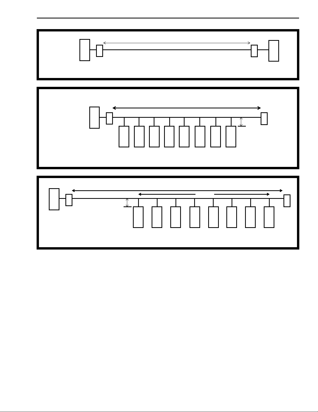
The MT8930C can interface to any of the three
wiring configurations which are specified by CCITT
Recommendation I.430 and ANSI T1.605 (refer to
Figs. 8 to 10). These consist of a point-to-point or
one of the two point-to-multipoint configurations (i.e.,
short passive bus or the extended passive bus). The
selection of line configurations is performed using
the timing bit (B4 of NT Mode Control Register).
For the short passive bus, TE devices are connected
at random points along the cable. However, for the
extended passive bus all connection points are
grouped at the far end of the cable from the NT.
Time out
BA =0
Pending
Deactivation
Send Info0
DR = 1
For an NT SNIC in fixed timing mode, the VCO and
Rx filters/peak detectors are disabled and the
threshold voltage is fixed. Ho w ever, for a TE SNIC or
an NT SNIC (in adaptive timing mode), the VCO and
Rx filters/peak detectors are enabled. In this
manner, the device can compensate for variable
round trip delays and line attenuation using a
threshold voltage set to a fixed percentage of the
pulse peak amplitude.
Another operation can be implemented using the
SNIC in the star configuration as shown in Figure 14.
This mode allows multiple NTs, with physically
independent S-Busses, to share a common input
source and transfer inf ormation down the S-Bus to all
9-42
NT
NT is operating in adaptive timing
TR is the line termination resistor = 100 Ω
T
R
Figure 8 - Point-to-Point Configuration
0 - 1 Km
100 m for 75 Ω impedance cable and 200 m for 150Ω impedance cable
100 - 200 m
MT8930C
T
R
TE
NT
NT is operating in fixed timing
TR is the line termination resistor = 100 Ω
T
R
TE
TE TE TE TE TE TE TE
Fiure 9 - Short Passive Bus Configuration, up to 8 TEs can be supported
NT
NT is operating in adaptive timing
TR is the line termination resistor = 100 Ω
T
R
0 - 10 m
TE TE TE TE TE TE TE
Figure 10 - Extended Passive Bus Configuration, up to 8 TEs can be supported
TEs . All NT devices connected into the star will
receive the information transmitted by all TEs on all
branches of the star, exactly as if they were on the
same physical S-Bus. All NTs in the star
configuration must be operating in fixed timing mode.
Refer to the description of the star configuration in
the ST-BUS section.
The SNIC has one last mode of operation called the
NT slave mode. This has the effect of operating the
SNIC in network termination mode (CK/NT pin = 1)
but having the frame structure and registers
description defined by the TE mode. This can be
used where multiple subscriber loops must carry a
fixed phase relation between each line. A typical
situation is when the system is trying to synchronize
two nodes of a synchronous network. This allows
multiple TEs to share a common ST-BUS timebase.
The synchronization of the loops is established by
using the clock signals produced by a local TE as an
input timing source to the NT slave.
T
0 - 10 m
0-500 m
0-50 m
R
T
R
TE
Adaptive Timing Operation
On power-up or after a reset, the SNIC in NT mode is
set to operate in fixed timing. To switch to adaptive
timing, the user should:
1) set the DR bit to 1
2) set the Timing bit to 1 in the C-channel
Control Register
3) wait for 100 ms period
4) proceed in using the AR and DR bits as
desired
Switching from adaptive timing mode is completed
by resetting the Timing bit.
9-43
MT8930C
125 µs
Channel0Channel
1
Channel
2
Bit 7 Bit 6 Bit 5 Bit 4 Bit 3 Bit 2 Bit 1 Bit 0
•••
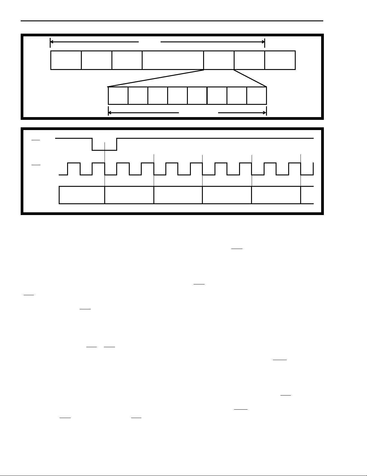
Figure 11 - ST-BUS Stream Format
F0b
C4b
ST-BUS
BIT CELLS
Channel 31
Bit 0
Channel 0
Bit 7
Figure 12 - Clock & Frame Alignment for ST-BUS Streams
ST-BUS Interface
The ST-BUS is a synchronous time division
multiplexed serial bussing scheme with data streams
operating at 2048 kbit/s configured as 32, 64 kbit/s
channels (refer to Fig. 11). Synchronization of the
data transfer is provided from a frame pulse which
identifies the frame boundaries and repeats at an 8
kHz rate. Figure 4 shows how the frame pulse
(F0b) defines the ST-BUS frame boundaries. All
data is clocked into the device on the rising edge of
the 4096 kHz clock (C4b) three quarters of the way
into the bit cell, while data is clocked out on the
falling edge of the 4096 kHz clock at the start of the
bit cell.
All timing signals (i.e. F0b & C4b) are identified as
bidirectional (denoted by the terminating b). The
I/O configuration of these pins is controlled by the
mode of operation (NT or TE). In the NT mode, all
synchronized signals are supplied from an external
source and the SNIC uses this timing while
transferring information to and from the S or
ST-BUS. In the TE mode, an on-board analog
phase-locked loop extracts timing from the received
data on the S-Bus and generates the system
4096 kHz (C4b) and frame pulse (F0b). The
analog phase-locked loop also maintains proper
phase relation between the timing signals as well as
filtering out jitter which may be present on the
received line port.
(8/2048) ms
Channel 0
Bit 6
Channel30Channel31Channel
Channel 0
Bit 5
0
Channel 0
Bit 4
When the TE mode is selected by tying the CK/NT
pin low, a continuous INFO0 signal on the receiver
will cause the PLL frequency to drift from its nominal
4.096 MHz value (C4b output). Hence, transmitted
INFO1 from the TE will not be at 192 kbps as
required in I.430 and T1.605. However, if the user’s
application requires the transmission of INFO1 at
exactly 192 kbit/s or the presence of an exact 4.096
MHz C4b clock at all times, then a 4.096 MHz clock
should be connected to the CK/NT pin.
This input clock serves to configure the device in TE
mode and to train the PLL in the absence of an
INFO2 or INFO4 signal on the line.
The SNIC uses the first four channels on the
ST-BUS (as shown in Figure 4). To simplify the
distribution of the serial stream, the SNIC
provides a delayed frame pulse (F0od) to eliminate
the need for a channel assignment circuit. This
signal is used to drive subsequent devices in the
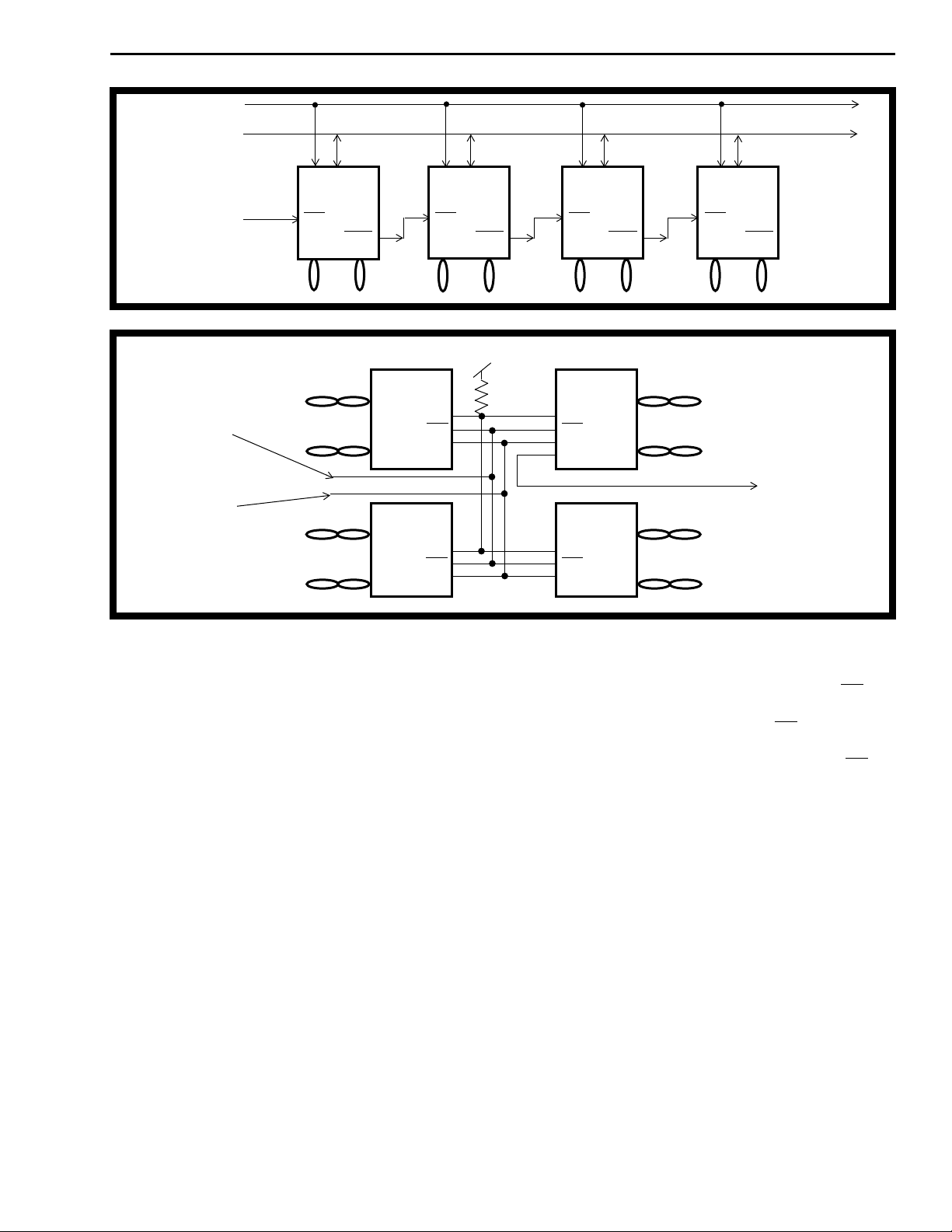
daisy chain (refer Figure 13). In this type of
arrangement, only the first SNIC in the chain will
receive the system frame pulse (F0b) with the
following devices receiving its predecessor’s delayed
output frame pulse (F0od).
The SNIC makes efficient use of its TDM bus
through the Star configuration. It does so by sharing
four common ST-BUS channels to multiple NT
devices.
9-44
ST-BUS Clock
ST-BUS
Stream
System
Frame Pulse
System
Frame Pulse
Input
ST-BUS Stream
Active on
Channel 0 - 3
MT8930C
NT
F0b
F0od
to TE to TE to TE to TE
MT8930C
F0b
Active on
Channels 4 - 7
NT
F0od
Active on
Channels 8 - 11
MT8930C
NT
F0b
F0od
Figure 13 - Daisy Chaining the SNIC
V
DD
to TE
to TE
MT8930C
NT
STAR
F0b
DSTi
MT8930C
NT
STAR
F0b
DSTi
MT8930C
NT
STAR
F0b
DSTi
DSTo
MT8930C
NT
STAR
F0b
DSTi
to TE
to TE
MT8930C
Active on
Channels 12 - 15
MT8930C
NT
F0b
F0od
Output
ST-BUS Stream
Figure 14 - NT in Star Configuration
Up to eight SNICs in NT mode with physically
independent S-Busses can be connected in parallel
to realize a star configuration, as shown in Figure 14.
All devices connected into the star will carry the
same input, thus information is sent to all TEs
simultaneously. The 2B+D data received from every
TE is transmitted to all NTs through the STAR pin.
Consequently, all the DSTo streams will carry
identical 2B+D data reflecting what is being
transmitted by the various TEs.
The flow of data in the direction of S-Bus to ST-BUS
is transparent to the SNIC, regardless of the state
machine status. On the other hand, the flow of data
in the direction of ST-BUS to S-Bus becomes
transparent only after the state machine is in the
active state (IS0, IS1=1,1), in case of an NT, or in the
synchronization state (IS0, IS1=1), in case of a TE.
Microprocessor/Control Interface
The parallel port on the SNIC operates as either a
general purpose microprocessor interface or as a
hardwired control port.
In microprocessor control mode (Cmode = 1), the
parallel port is compatible with either Motorola or
Intel multiplexed bus signals and timing. The
MOTEL circuit (MOtorola and InTEL
Compatible bus) uses the level of the DS/RD pin
at the rising edge of AS/ALE to select the
appropriate bus timing. If DS/RD is low at the
rising edge of AS/ALE (refer Fig. 26) then Motorola
bus timing is selected. Conversely, if DS/RD is
high at the rising edge of AS/ALE (refer Figs. 24 &
25), then Intel bus timing is selected. This has the
effect of redefining the microprocessor port
transparently to the user.
In this mode, the user has the option of writing to the
C-channel Control or Diagnostic Register through
the parallel port interface or through the C-channel
on DSTi. Bit 0 of the Master Control Register
provides this option.
The parallel port on the SNIC allows complete
control of the HDLC transceiver and access to all
data, control and status registers. The internal
registers (defined in Table 2) can be accessed
through the microprocessor port only when the
Cmode pin is held high. Reading these registers
allows the microprocessor to monitor incoming data
on the S or ST-BUS without interrupting the nor mal
data flow.
9-45
 Loading...