MITEL MT8816AC, MT8816AE, MT8816AP Datasheet

ISO-CMOS
8 x 16 Analog Switch Array
MT8816
Features
• Internal cont rol lat ches and add ress d eco der
• Short set-up and hold times
• Wide ope rating v oltag e: 4. 5V to 13.2V
• 12Vpp anal og s ignal capabi lity
•R
• ∆R
65Ω max. @ VDD=12V, 25°C
ON
≤10Ω @ VDD=12V, 25°C
ON
• Full CMOS switch for low distortion
• Minimum f eedthr oug h and c ros stal k
• Separate ana lo g and di gital re ferenc e supp lies
• Low power consumption ISO-CMOS technology
Applications
• Key systems
• PBX systems
• Mobile rad io
• Test e quipme nt/ instr umen tatio n
• Analo g/ di gita l m ult ip le xers
• Audio/Video switching
ISSUE 2 November 1988
Ordering Information
MT8816AC 40 Pin Ce r am i c D IP
MT8816AE 40 Pin Pla stic D IP
MT8816AP 44 Pin PL C C
-40° to 85°C
Description
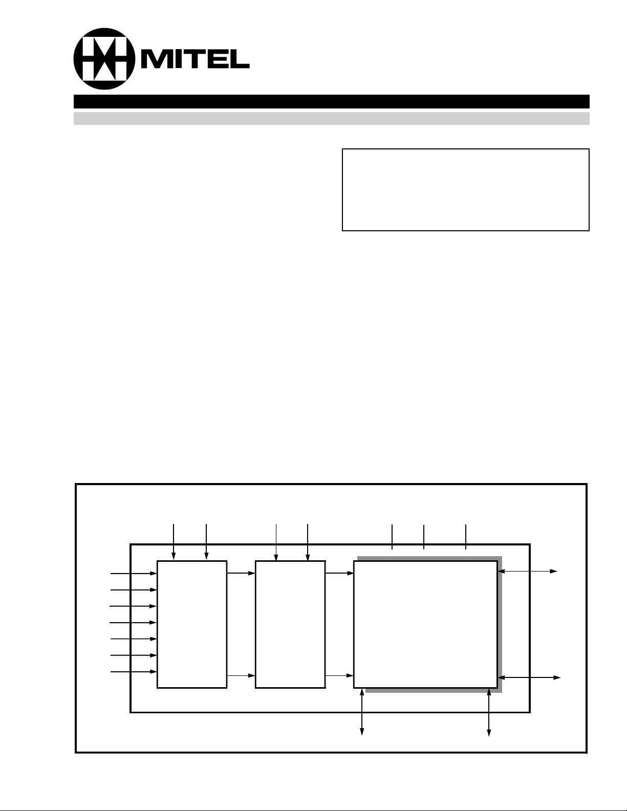
The Mitel MT8816 is fabricated in MITEL’s ISOCMOS technology providing low power dissipation
and high reliability. The device contains a 8 x 16
array of crosspoint switches along with a 7 to 128
line decoder and latch circuits. Any one of the 128
switches can be addressed by selecting the
appropriate seven address bits. The selected switch
can be turned on or off by applying a logical one or
zero to the DATA in p ut . V
of the digital inputs. The range of the analog signal
is from V
to VEE. Chip Select (CS) allows the
DD
crosspoint array to be cascaded for matrix
expansion.
is the ground refer-ence
SS
AX0
AX1
AX2
AX3
AY0
AY1
AY2
CS STROBE DATA RESET VDD VEE VSS
11
8 x 16
7 to 128
Decoder
Latches
Switch
Array
128128
• • • • • • • • • • • • • • • • • • •
Yi I/O (i=0-7)
Figure 1 - Functional Block Diagram
• • • • • • • • • • • • • • • •
Xi I/O
(i=0-15)
3-45

MT8816 ISO-CMOS
1
Y3
AY2
RESET
AX3
AX0
VSS
STROBE
VEE
2
3
4
5
6
X14
7
X15
8
X6
9
X7
10
X8
11
X9
12
X10
13
X11
14
NC
15
Y7
16
17
Y6
18
19
Y5
20
40 PIN CERDIP/PLASTIC DIP 44 PIN PLCC
40
39
38
37
36
35
34
33
32
31
30
29
28
27
26
25
24
23
22
21
VDD
Y2
DATA
Y1
CS
Y0
NC
X0
X1
X2
X3
X4
X5
X12
X13
AY1
AY0
AX2
AX1
Y4
X14
X15
X6
X7
X8
X9
X10
X11
NC
NC
Y7
DATA
Y2
VDD
Y3
AY2
RESET
AX3
AX0
NC
65432 44434241
7
8
9
10
11
12
13
14
15
16
17
Y6
VSS
1
231819202122 242526 2728
Y5
VEE
STROBE
Y4
AX1
AX2
AY0
Y1
40
39
38
37
36
35
34
33
32
31
30
29
AY1
CS
NC
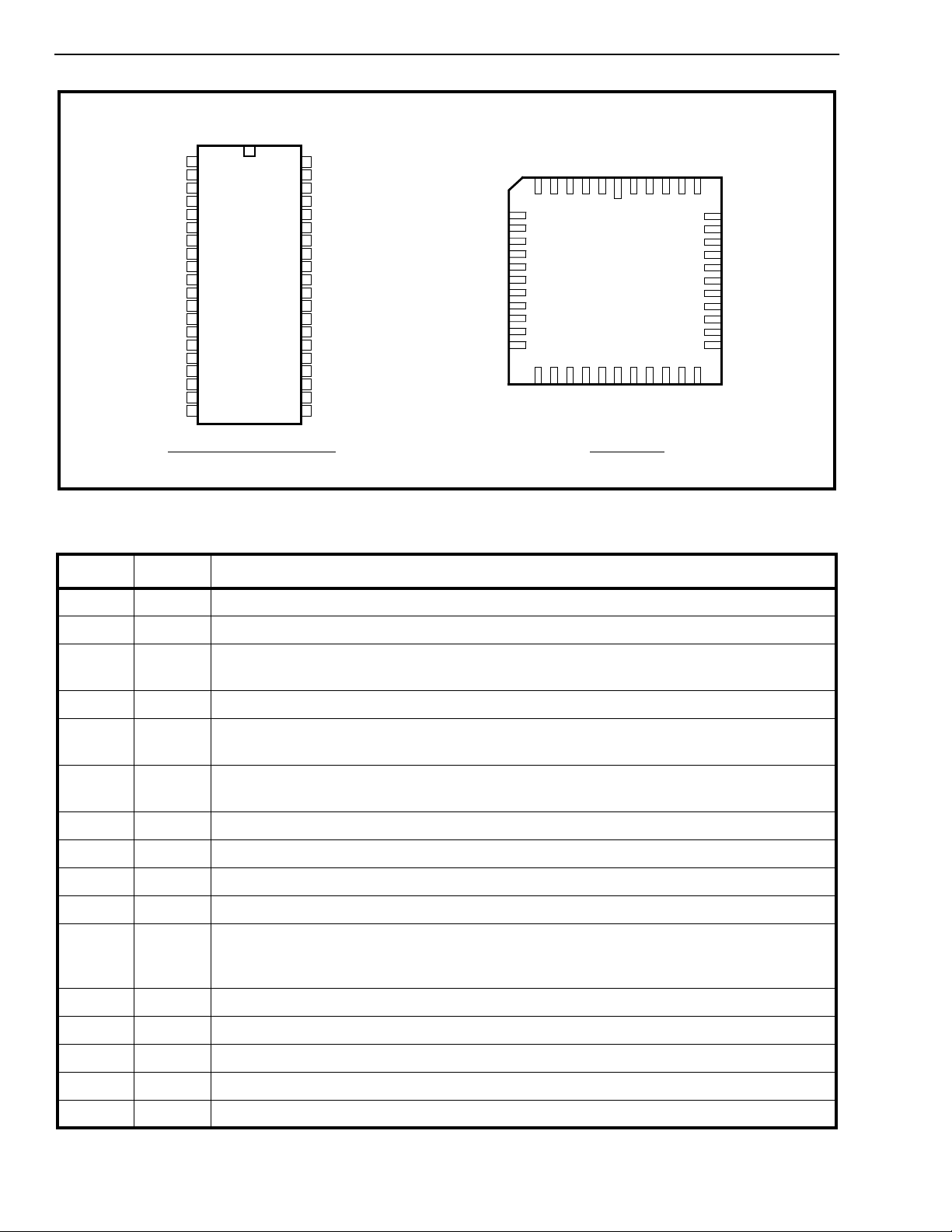
Figure 2 - Pin Connections
Pin Description
Pin #* Name Description
1Y3Y3 Analog (Input/Output): this is connected to the Y3 column of the switch array.
Y0
NC
X0
X1
X2
X3
X4
X5
X12
X13
NC
2AY2Y2 Add ress Lin e (Inp ut).
3 RESET Master RESET (Input): this is used to turn off all switches regardless of the condition of
CS. Active High.
4,5 AX3,AX0 X3 and X0 Address Lines (Inputs).
6,7 X14, X15 X14 and X15 Analog (Inputs/Outputs): these are connected to the X14 and X15 rows of
the switch array.
8-13 X6-X11 X6-X11 Analog (Inputs/Outputs): these are connected to the X6-X11 rows of the switch
array.
14 NC No Connection
15 Y7 Y7 Analog (Input/Output): this is connected to the Y7 column of the switch array.
16 V
Digital Ground Reference.
SS
17 Y6 Y6 Analog (Input/Output): this is connected to the Y6 column of the switch array.
18 STROB E STROBE (Input): enables function selected by address and data. Address must be stable
before STRO BE goes high and DATA must be stable on the falling edge of the STROBE .
Active High.
19 Y5 Y5 Analog (Input/Output): this is connected to the Y5 column of the switch array.
20 V
Negative Power Supply.
EE
21 Y4 Y4 Analog (Input/Output): this is connected to the Y4 column of the switch array.
22, 23 AX1,AX2 X1 and X2 Address Lines (Inputs).
24, 25 AY0,AY1 Y0 and Y1 Address Lines (Inputs).
* Plastic DIP and CERDIP only
3-46
 Loading...