MITEL MT8812AP, MT8812AC, MT8812AE, SP5659MP1T Datasheet

The SP5659 is a single chip frequency synthesiser designed
for tuning systems up to 2·7GHz.
The RF preamplifier drives a divide-by two prescaler which
can be disabled for applications up to 2GHz, allowing direct
interfacing with the programmable divider, resulting in a step
size equal to the comparison frequency. For applications up
to 2·7GHz the divide-by two is enabled to give a step size of
twice the comparison frequency.
The comparison frequency is obtained either from an onchip crystal controlled oscillator or from an external source.
The oscillator frequency F
REF
or the comparison frequency
F
COMP
may be switched to the REF/COMP output; this feature
is ideally suited to providing the reference frequency for a
second synthesiser such as in a double conversion tuner (see
Fig. 5).
The synthesiser is controlled via an I
2
C bus and responds
to one of four programmable addresses which are selected by
applying a specific voltage to the Address input. This feature
enables two or more synthesisers to be used in a system.
The SP5659 contains four switching ports, P0-P3 and a
5-level ADC, the output of which can be read via the I
2
C bus.
The SP5659 also contains a varactor line disable and
charge pump disable facility.
FEATURES
■ Complete 2·7GHz Single Chip System
■ Optimised for Low Phase Noise
■ Selectable 42 prescaler
■ Selectable Reference Division Ratio
■
Selectable Reference/Comparison Frequency Output
■ Selectable Charge Pump Current
■ Varactor Drive Amplifier Disable
■ 5-Level ADC
■ Variable I
2
C BUS Address for Multi-tuner Applications
SP5659
2·7GHz I2C Bus Low Phase Noise Synthesiser
Preliminary Information
Supersedes March 1996 version, DS4206-1.8 DS4296 - 2.0 June 1998
SP5659
1
2
3
4
5
6
7
8
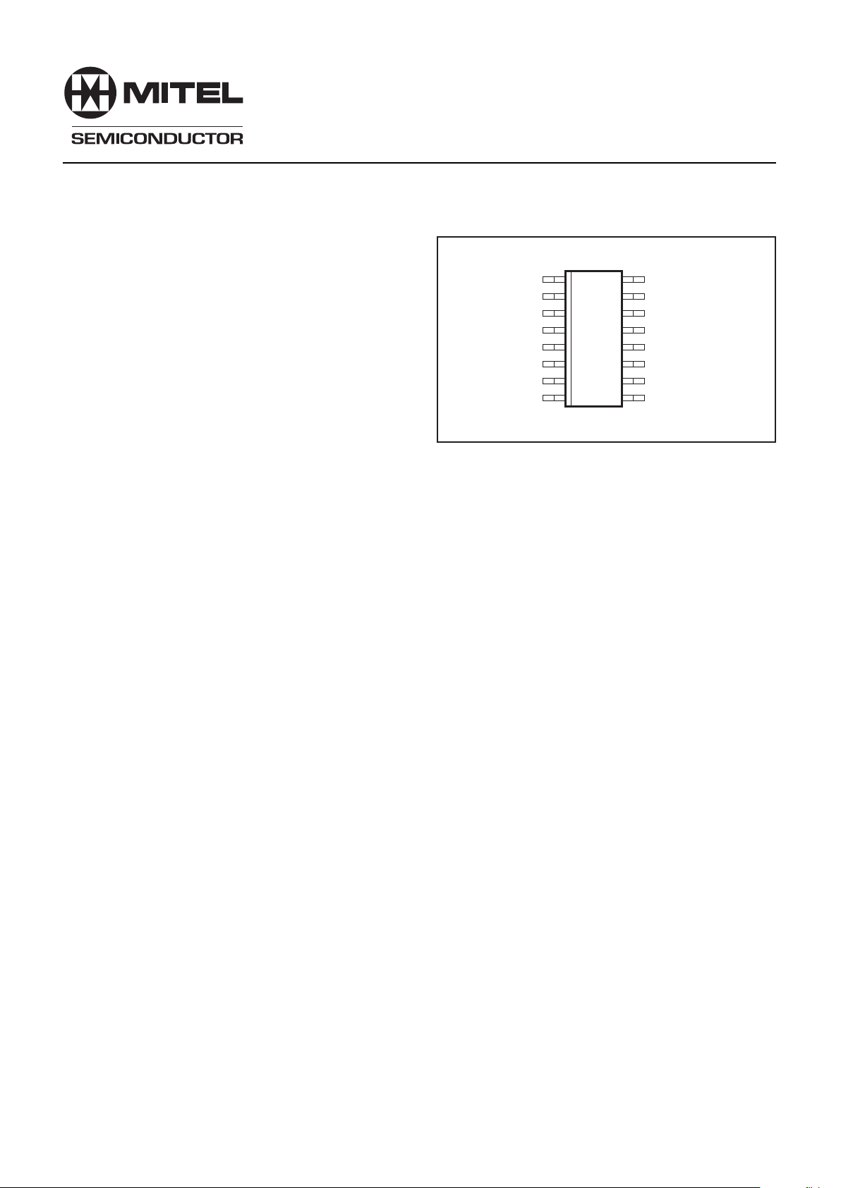
MP16
16
15
14
13
12
11
10
9
CHARGE PUMP
CRYSTAL
REF/COMP
ADDRESS
SDA
SCL
PORT P3
PORT P2
DRIVE
V
EE
RF INPUT
RF INPUT
V
CC
ADC
PORT P0
PORT P1
Fig. 1 Pin connections – top view
■ ESD Protection: 4kV, Mil-Std-883C, Method 3015
(1)
■ Pin Compatible with SP5658
(1) Normal ESD handling precautions should be observed.
APPLICATIONS
■ Satellite TV
■ High IF Cable Tuning Systems
THERMAL DATA
u
JC
= 41°C/W
u
JA
= 111°C/W
ORDERING INFORMATION
SP5659 KG/MP1S (Tubes)
SP5659 KG/MP1T (Tape and reel)

2
SP5659
ELECTRICAL CHARACTERISTICS
T
AMB
= 220°C to 180°C, V
CC
= 14·5V to 15·5V, reference frequency = 4MHz.
These Characteristics are guaranteed by either production test or design. They apply within the specified ambient temperature
and supply voltage ranges unless otherwise stated.
Supply current, I
CC
RF input voltage
RF input impedance
RF input capacitance
SDA, SCL
Input high voltage
Input low voltage
Input high current
Input low current
Leakage current
Input hysteresis
SDA
Output voltage
Charge Pump
Output current
Output leakage current
Drive output current
Drive saturation voltage
External reference input frequency
External reference input amplitude
Crystal frequency
Crystal oscillator drive level
Recommended crystal series resistance
Crystal oscillator negative resistance
REF/COMP output voltage, enabled
Comparison frequency
Equivalent phase noise at phase detector
RF division ratio
Reference division ratio
P0, P1, P2, P3 sink current
P0, P1, P2, P3 leakage current
ADC input voltage
ADC input current
Address input current high
Address input current low
Typ.
Value
12
13,14
13,14
13,14
5, 6
5, 6
5, 6
5, 6
5, 6
5, 6
5
1
1
16
16
2
2
2
2
2
3
7,8,9,10
11
11
4
4
50
3
0
1
2
200
4
35
10
400
240
480
10
68
58
50
2
0·8
63
350
2142
85
73
300
5·5
1·5
10
210
10
0·4
610
350
200
20
500
16
200
2
131071
262142
10
610
1
20·5
Min. Max.
mA
mA
mVrms
mVrms
mVrms
Ω
pF
V
V
µA
µA
µA
V
V
nA
mA
mV
MHz
mVp-p
MHz
mVp-p
Ω
Ω
mVp-p
MHz
dBC/Hz
mA
µA
µA
mA
mA
V
CC
= 5V, PE = 1 (note 1)
V
CC
= 5V, PE = 0
300MHz to 2·7GHz, PE = 1
(prescaler enabled) see Fig. 4b
100MHz, PE = 1 (prescaler
enabled) see Fig. 4b
100MHz to 2·0GHz, PE = 0
(prescaler disabled) see Fig. 4b
See Fig. 10
See Fig. 10
Input voltage = V
CC
Input voltage = V
EE
VCC = V
EE
Sink current = 3mA
Drive output disabled
AC coupled sinewave
AC coupled sinewave
Parallel resonant crystal (note 2)
Includes temperature and process
tolerances
AC coupled, RE = 1, see note 3
See note 4
Prescaler disabled, see Table 1
Prescaler enabled, see Table 1
See Table 1
V
PORT
= 0·7V
V
PORT
= 13·2V
See Fig. 3 Table 5
V
CC >VINPUT >VEE
Input voltage = V
CC
Input voltage = V
EE
Characteristic Pin Units Conditions
NOTES
1. Maximum power consumption is 468mW with V
CC
= 5·5V and all ports off.
2. Resistance specified is maximum under all conditions including start up.
3. If the REF/COMP output is not used, it should be left open circuit or connected to V
CC
and disabled by setting RE to logic 0.
4. 6kHz loop bandwidth, phase comparator frequency 250kHZ. Figure measured at 1kHz offset DSB (within loop bandwidth).

3
SP5659
Supply voltage
RF input voltage
RF input DC offset
Port voltage
Total port current
ADC input DC offset
REF/COMP output DC offset
Charge pump DC offset
Drive DC offset
Crystal oscillator DC offset
Address DC offset
SDA, SCL input voltage
Storage temperature
Junction temperature
Port in off state
Port in on state
12
13,14
13, 14
7-10
7-10
7-10
11
3
1
16
2
4
5, 6
ABSOLUTE MAXIMUM RATINGS
All voltages are referred to VEE at 0V
Max.Min.
7
2·5
V
CC
10·3
14
6
50
V
CC
10·3
VCC10·3
V
CC
10·3
V
CC
10·3
VCC10·3
V
CC
10·3
6
1150
1150
Value
20·3
20·3
20·3
20·3
20·3
20·3
20·3
20·3
20·3
20·3
255
V
V p-p
V
V
V
mA
V
V
V
V
V
V
V
°C
°C
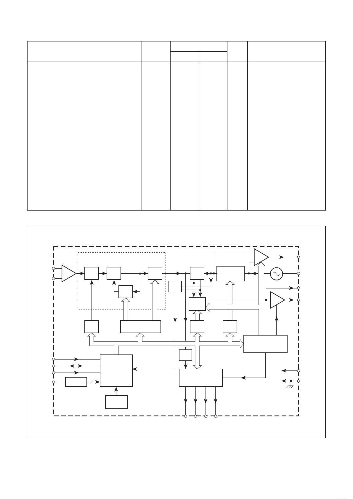
Fig. 2 Block diagram
RF IN
ADDRESS
SDA
LOCK
DET
42/1
13
14
4
5
F
COMP
CHARGE
PUMP
CRYSTAL
2
OSC
789
10
P3 P2 P1 P0
F
PD
416/17
4-BIT
COUNT
13-BIT
COUNT
PROGRAMMABLE DIVIDER
PREAMP
17-BIT LATCH
DIVIDE RATIO
1-BIT
COUNT
PE
PHASE
COMP
I2C
TRANSCEIVER
SCL
6
CHARGE
PUMP
2-BIT
LATCH
FPD/2
3-BIT ADC
ADC
11
3
POWER ON
DETECT
4-BIT LATCH
AND
PORT INTERFACE
REFERENCE
DIVIDER
(SEE TABLE 1)
REF/COMP
3
2-BIT
LATCH
V
CC
V
EE
15
C1, C0
F
L
F
REF
5-BIT LATCH AND
MODE CONTROL LOGIC
(SEE TABLE 6)
DISABLE
DRIVE
16
1
MODE
CONTROL
P0 TEST
CONTROL
12
Parameter Pin Units Conditions

4
SP5659
FUNCTIONAL DESCRIPTION
The SP5659 contains all the elements necessary – with
the exception of a frequency reference, loop filter and external
high voltage transistor – to control a varactor tuned local
oscillator, so forming a complete PLL frequency synthesised
source. The device allows for operation with a high comparison
frequency and is fabricated in high speed logic which enables
the generation of a loop with good phase noise performance.
The block diagram is shown in Fig. 2.
The RF input signal is fed to an internal preamplifier, which
provides gain and reverse isolation from the divider signals.
The output of the preamplifier interfaces with a 17-bit fully
programmable divider via a 42 prescaler. For applications up
to 2·0GHz RF input, the prescaler can be disabled, so
eliminating the degradation in phase noise due to prescaler
action. The divider is of MN1A architecture, where N = 16 or
17, the M counter is 13 bits and the A counter is 4 bits.
The output of the programmable divider, F
PD
, is fed to the
phase comparator where it is compared in phase and frequency
domains with the comparison frequency F
COMP
. This frequency
is derived either from the on-chip crystal controlled oscillator
or from an external reference source. In either case, the
reference frequency F
REF
is divided down to the comparison
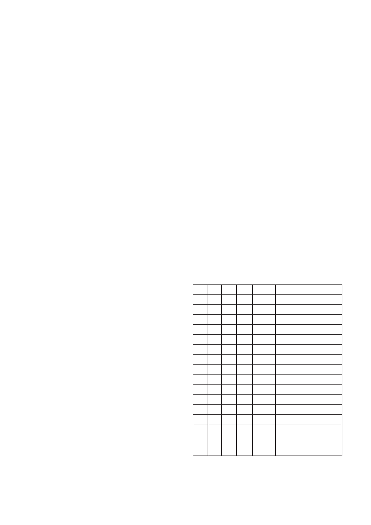
frequency by the reference divider, which is programmable to
one of 15 ratios as detailed in Table 1.
The output of the phase detector feeds a charge pump and
loop amplifier section which, when used with an external high
voltage transistor and loop filter, integrates the current pulses
into the varactor line voltage. By invoking the device test
modes as described in Fig. 3, Table 6, the varactor drive
output can be disabled, so switching the external transistor
off. This allows an external voltage to be applied to the
varactor line for tuner alignment purposes. Similarly, the
charge can also be disabled to a high impedance state.
The programmable divider output F
PD
/2 can be switched to
port P0 by programming the device into test mode as set out
in Table 6.
PROGRAMMING
The SP5659 is controlled by an I2C Bus. Data and Clock
are fed in on the SDA and SCL lines respectively, as defined
by the I
2
C Bus format. The synthesiser can either accept new
data (write mode) or send data (read mode). The LSB of the
address byte (R/W) sets the device into write mode if it is low
and read mode if it is high. Tables 1 and 2 in Fig. 3 illustrate
the format of the data. The device can be programmed to
respond to several addresses, which enables the use of more
than one synthesiser in an I
2
C Bus system. Table 4 in Fig. 3
shows how the address is selected by applying a voltage to
the address input.
When the device receives a valid address byte, it pulls the
SDA line low during the acknowledge period, and during
following acknowledge periods after further data bytes are
programmed. When the device is programmed into the read
mode, the controller accepting the data must pull the SDA line
low during all status byte acknowledge periods to read another status byte. If the controller fails to pull the SDA line low
during this period, the device generates an internal STOP
condition, which inhibits further reading.
WRITE Mode (Frequency Synthesis)
With reference to Table 2, bytes 2 and 3 contain frequency
information bits 214 to 20 inclusive. Auxiliary frequency bits 2
16
and 215 are in byte 4. For most frequencies, only bytes 2 and
3 will be required. The remainder of byte 4 and byte 5 control
the prescaler enable, reference divider ratio (see Fig. 3),
output ports and test modes (see Table 6).
After reception and acknowledgment of a valid address
(byte 1), the first bit of the following byte determines whether
the byte is interpreted as byte 2 (logic ‘0’) or byte 4 (logic ‘1’);
the next data byte is then interpreted as byte 3 or byte 5,
respectively. After two complete data bytes have been received, additional data bytes can be entered, where byte
interpretation follows the same procedure without readdressing the device. This procedure continues until a STOP condition is received. The STOP condition can be generated after
any data byte; if, however, it occurs during a byte transmission then the previous data is retained.
To facilitate smooth fine tuning, the frequency data bytes are
only accepted by the device after all 17 bits of the data have
been received or after the generation of a STOP condition.
Repeatedly sending bytes 2 and 3 only will not change the
frequency. A frequency change when one of the following
data sequences is sent to an addressed device:
Bytes 2, 3, 4, 5
Bytes 4, 5, 2, 3
or when a STOP condition follows valid data bytes thus:
Bytes 2, 3, 4, STOP
Bytes 4, 5, 2, STOP
Bytes 2, 3, STOP
Bytes 2, STOP
Bytes 4, STOP
It should be noted that the SP5569 must be addressed
initially with both frequency AND control byte data, since the
control byte contains reference divider information which
must be provided before a chosen frequency can be synthesised. This implies that after initial turn on, bytes 2, 3 and 4
must be sent followed by a STOP condition as a minimum
requirement. Alternatively, bytes 2, 3, 4 and 5 must be sent if
port information is also required.
READ Mode
When the device is in read mode the status byte read from
the device on the SDA line takes the form shown in Fig. 3,
Table 3.
Bit 1 (POR) is the power-on reset indicator and is set to a
logic ‘1’ if the V
CC
supply to the device has dropped below 3V
(at 25˚C), for example, when the device is initially turned on.
R2
0
0
0
0
1
1
1
1
0
0
0
0
1
1
1
1
R3
0
0
0
0
0
0
0
0
1
1
1
1
1
1
1
1
R1
0
0
1
1
0
0
1
1
0
0
1
1
0
0
1
1
Comparison frequency
2MHz
1MHz
500kHz
250kHz
125kHz
62·5kHz
31·25kHz
15·625kHz
800kHz
400kHz
200kHz
100kHz
50kHz
25kHz
12·5kHz
R0
0
1
0
1
0
1
0
1
0
1
0
1
0
1
0
1
Ratio
2
4
8
16
32
64
128
256
Invalid
5
10
20
40
80
160
320
Table 1 Reference division ratios (4MHz external reference)
 Loading...