MITEL MT8808 Technical data

查询MT8808供应商
ISO-CMOS
MT8808
8 x 8 Analog Switch Array
Features
• Internal cont rol lat ches and add ress d eco der
• Short set-up and hold times
• Wide ope rating v oltag e: 4. 5V to 13.2V
• 12Vpp anal og s ignal capabi lity
•R
• ∆R
65Ω max. @ VDD=12V, 25°C
ON
≤ 10Ω @ VDD=12V, 25°C
ON
• Full CMOS switch for low distortion
• Minimum f eedthr oug h and c ros stal k
• Separate ana lo g and di gital re ferenc e supp lies
• Low power consumption ISO-CMOS technology
Applications
• Key systems
• PBX systems
• Mobile rad io
• Test equipment /instru men tatio n
• Analo g/ di gita l m ult ip le xers
• Audio/Video switching
ISSUE 2 November 1988
Ordering Information
MT8808AC 28 Pin Ce r am i c D IP
MT8808AE 28 Pin Pla stic D IP
MT8808AP 28 Pin PL C C
-40° to 85°C
Description
The Mitel MT8808 is fabricated in MITEL’s ISOCMOS technology providing low power dissipation
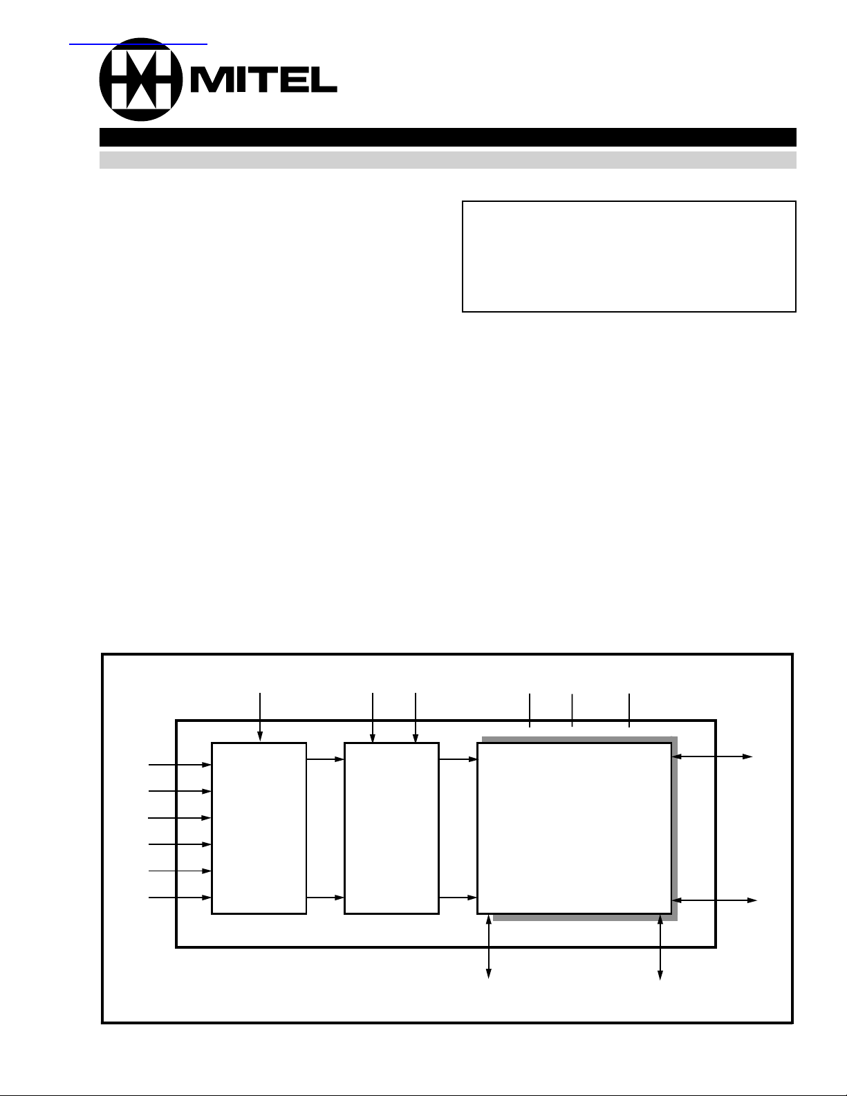
and high reliability. The device contains a 8 x 8 array
of crosspoint switches along with a 6 to 64 line
decoder and latch circuits. Any one of the 64
switches can be addressed by selecting the
appropriate six address bits. The selected switch can
be turned on or off by applying a logical one or zero
to the DATA input. V
the digital inputs. The range of the analog signal
is from V
to VEE.
DD
is the ground reference of
SS
AX0
AX1
AX2
AY0
AY1
AY2
STROBE DATA RESET VDD VEE VSS
11
8 x 8
6 to 64
Decoder
Latches
Switch
Array
6464
• • • • • • • • • • • • • • • • • • •
Yi I/O (i=0-7)
Figure 1 - Functional Block Diagram
• • • • • • • • • • • • • • • •
Xi I/O
(i=0-7)
3-15

MT8808 ISO-CMOS
X0
X2
X4
X6
Y7
Y6
Y5
Y4
1
2
3
4
5
6
7
8
9
10
11
12
13
14
AY2
STROBE
VEE
DATA
VSS
RESET
28
27
26
25
24
23
22
21
20
19
18
17
16
15
AY1
AY0
AX2
AX1
AX0
X1
X3
X5
X7
VDD
Y0
Y1
Y2
Y3
VSS
X0
X2
X4
X6
RESET
Y7
5
6
7
8
9
10
11
E
B
O
A
T
E
A
E
D
V
4
3
3
2
1
1
6
5
Y
Y
0
1
2
R
T
S
2
•
4
1
4
Y
2
Y
Y
X
Y
A
A
A
A
8
1
6
7
2
2
2
AX1
25
AX0
24
X1
23
22
X3
21
X5
20
X7
19
6
5
7
1
1
1
2
3
1
Y
Y
Y
VDD
8
1
0
Y
28 PIN CERDIP/PLASTIC DIP
28 PIN PLCC
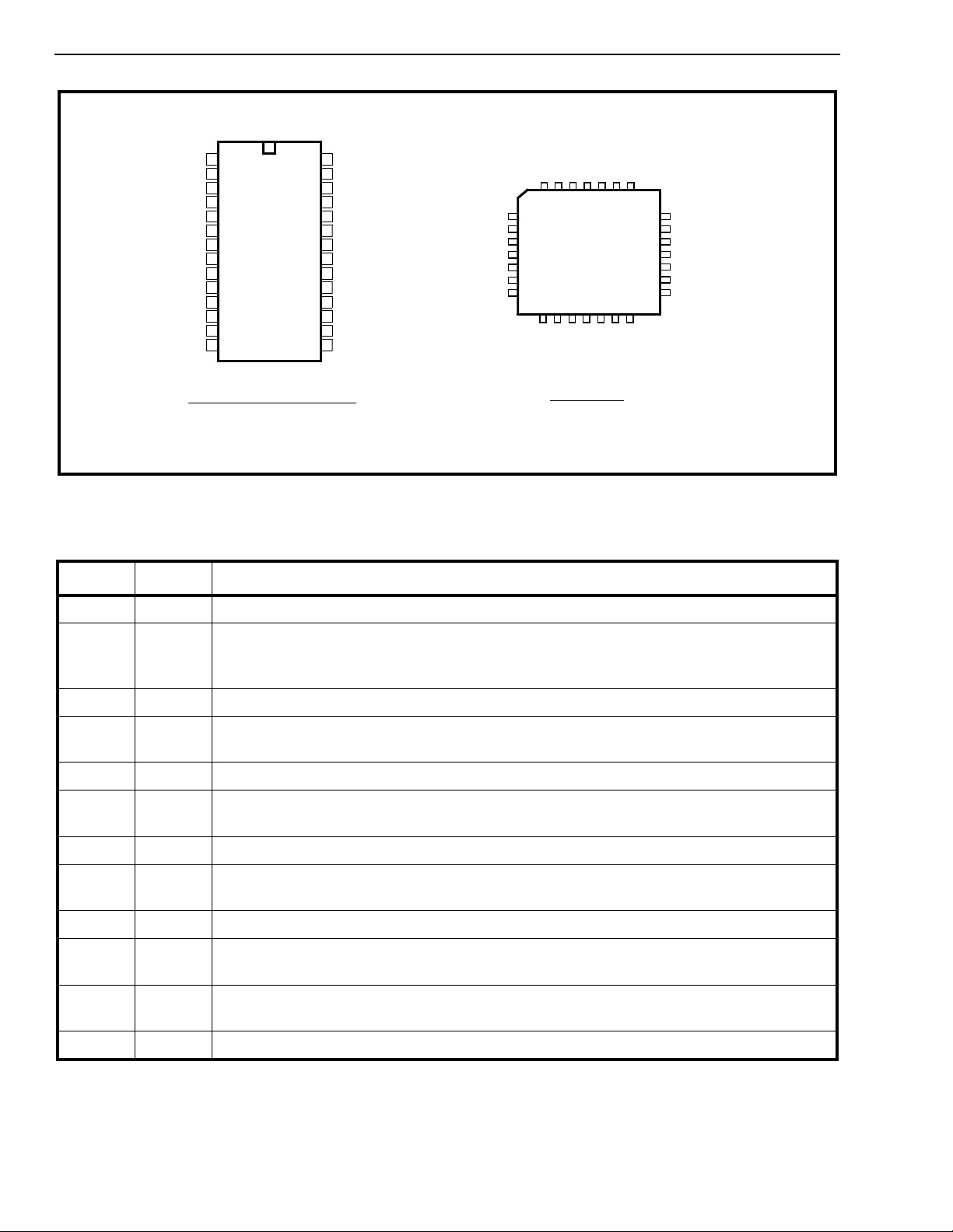
Figure 2 - Pin Connections
Pin Description
Pin # Name Description
1AY2AY2 Address Line (Input).
2STROBESTROBE (Input): enables function selected by address and data. Address must be stable
before STROBE goes high and DATA must be stable on the falling edge of the STROBE .
Active High.
3V
4DATADATA (Input): a logic high input will turn on the selected switch and a logic low will turn off
5V
6-9 X0, X2,
X4, X6
Negative Power Supply.
EE
the selected switch. Active High.
Digital Ground Reference .
SS
X0, X2, X4 and X6 Analog (Inputs/Outputs): these are connected to the X0, X2, X4 and
X6 rows of the switch array.
10 RESET Master RESET (Input): this is used to turn off all swit ches. Active High.
11-18 Y7 - Y0 Y7 - Y0 Analog (Inputs/Outputs): these are connected to the Y0 - Y7 columns of the
switch array.
19 V
20-23 X7, X5,
X3, X1
24-26 AX0-
Positive Power Sup pl y.
DD
X7, X5, X3 and X1 Analog (Inputs/Outputs): these are connected to the X7, X5, X3 and
X1 rows of the switch array.
AX0 - AX2 Address Lines (Inputs).
AX2
27,28 A Y0, AY1 AY0 and AY1 Address Lines (Inputs).
3-16
 Loading...