MITEL MT8804AP, MT8804AC, MT8804AE Datasheet

8 x 4 Analog Switch Array
CMOS
MT8804A
Features
• Micro p r ocessor com p atible c ontro l inpu ts
• On chip cont rol mem ory an d addre ss de cod ing
• Row address ing
• Master reset
• 32 crosspoint switches in 8 x 4 array
• 5.0V to 15.0V operation
• Low crosstalk between switches
• Low on resistance: 90Ω (typ.) at 13V
• Matched switch characteristics
• Switches fre quenc ies up to 40 MHz
Applications
• PABX and key sytems
• Data acquisition systems
• Test equipme nt/in strum ent ation
• Analog / dig ita l mu lt ip lex ers
ISSUE 2 October 1989
Ordering Information
MT8804AC 24 Pin Ce r am i c D IP
MT8804AE 24 Pin Pla stic D IP
MT8804AP 28 Pin PL C C
-40° to 85°C
Descript ion
The MT8804A is a CMOS/LSI 8 x 4 Analog Switch
Array incorporating control memory (32 bits), decoder and digital logic level converters. This circuit has
digitally controlled analog switches having very low
“ON“ resistance and very low “OFF” leakage current.
Switches will operate with analog signals at
frequencies to 40 MHz and up to 15.0Vp-p. A
“HIGH“ on the Master Reset input switches all
channels “OFF“ and clears the memory. This device
is ideal for crosspoint switching applications.
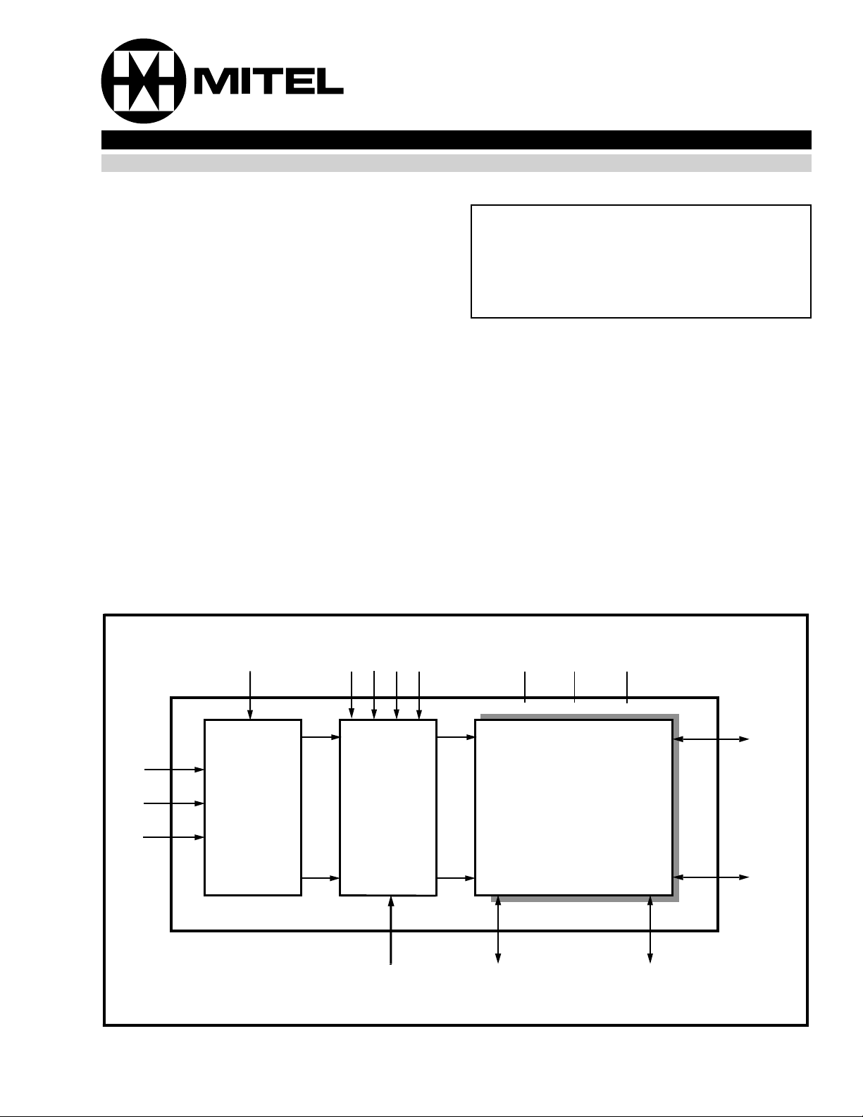
A0
A1
A2
AE D0 D1 D2 D3 VDD VEE VSS
11
3 to 8
Decoder
Latches
832
• • • • • • • • • • • • • • • • • • •
MR Ji I/O (i=0-3)
8 x 4
Switch
Array
Figure 1 - Functional Block Diagram
• • • • • • • • • • • • • • • •
Li I/O
(i=0-7)
3-3
3-3

MT8804A CMOS
1
L2
2
L1
3
L0
4
D0
5
J0
D1
6
J1
7
D2
8
J2
9
D3
10
J3
VSS
11
12
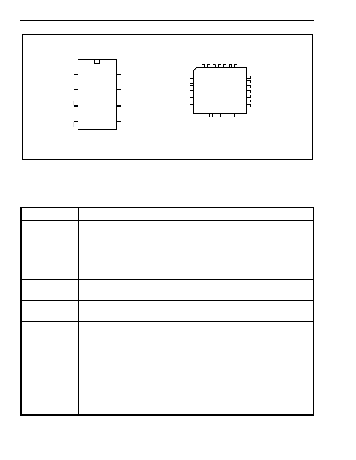
24 PIN CERDIP/PLASTIC DIP
24
23
22
21
20
19
18
17
16
15
14
13
VDD
L3
L4
L5
L6
L7
MR
AE
A2
A1
A0
VEE
NC
D0
J0
D1
J1
D2
J2
Figure 2 - Pin Connections
Pin Description
Pin #* Name Description
C
N
4
5
6
7
8
9
10
11
2
1
3
D
28 PIN PLCC
D
D
1
0
L
3
3
1
3
J
3
4
2
L
L
V
L
L
2
8
7
1
6
2
2
2
•
4
7
6
5
1
1
1
1
0
1
E
S
A
A
E
S
V
V
L5
25
L6
24
23
L7
22
MR
21
AE
20
A2
19
NC
8
1
C
N
1-3 L2-L0 L2-L0 Analog Lines (Inputs/Outputs): these are connected to the L2-L0 columns of the
switch array.
4D0D0 Data (Input): Active High.
5J0J0 Analog Junctor (Input/Output): this is connected to the J0 row of the switch array.
6DIDI Data (Input). Active High.
7J1J1 Analog Junctor (Input/Output): this is connected to the J1 row of the switch array.
8D2D2 Data (Input): Active High.
9J2J2 Analog Junctor (Input/Output): this is connected to the J2 row of the switch array.
10 D3 D3 Data (Input): Active High.
11 J3 J3 Analog Junctor (Input/Output): this is connecte d to the J3 row of the switch array.
12 V
13 V
Digital Ground Reference.
SS
Negative Power Suppl y.
EE
14-16 A0-A2 A0-A2 Addr ess Lines (In pu ts) .
17 AE Add ress En abl e/ Str obe (Inpu t): enables function select ed by address and data. Address
must be stable before AE goes high and D0-D3 must be stabl e on the falling edge of the
AE. Active High.
18 MR Master RESET (Input): this is used to turn off all switches. Active Hig h.
19-23 L7-L3 L7-L3 Analog Lines (Inputs/Outputs): these are connected to the L7-L3 columns of the
switch array.
24 V
Positive P ow er Su pp ly.
DD
* Plastic DIP and CERDIP only
3-4
 Loading...