MITEL MH8981DE, MH8981DL, MH8981DP, MH8981DC Datasheet

2-17
Features
• Mitel ST-BUS compatibl e
• 4-line x 32-c hanne l inpu ts
• 4-line x 32-c hanne l outpu ts
• 128 ports non-blocking switch
• Single power s upp ly (+5 V )
• Low power co nsu mpt ion: 30 m W Typ.
• Microprocess o r-c on t rol i nterface
• Three-state serial outputs
Description
This VLSI ISO-CMOS device is designed for
switching PCM-encoded voice or data, under
microprocessor control, in a modern digital
exchange, PBX or Central Office. It provides
simultaneous connections for up to 128 64 kbit/s
channels. Each of the four serial inputs and outputs
consist of 32 64 kbit/s channels multiplexed to form a
2048 kbit/s ST-BUS stream. In addition, the MT8981
provides microprocessor read and write access to
individual ST-BUS channels.
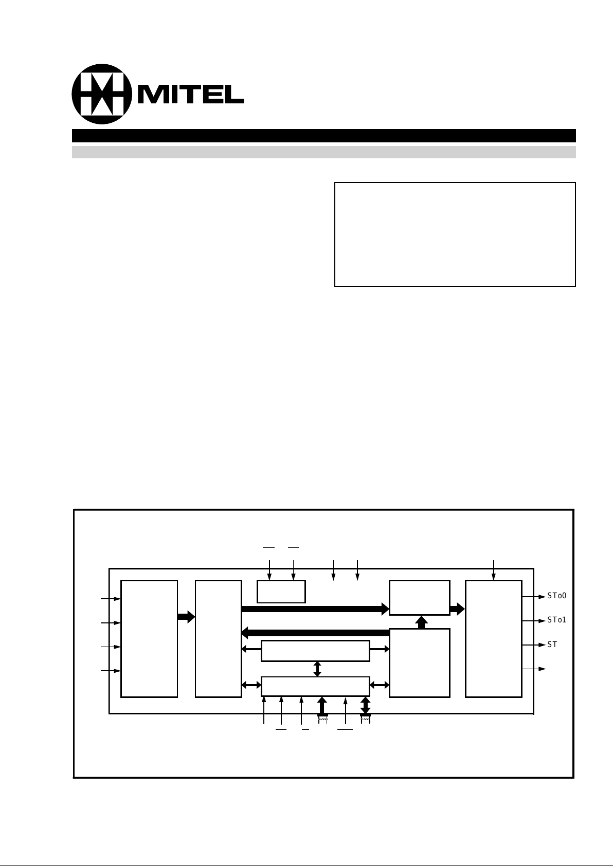
Figure 1 - Functional Block Diagram
STo0
STo1
STo2
STo3
Serial
to
Parallel
Converter
Data
Memory
Frame
Counter
Control Register
Control Interface
Output
MUX
Connection
Memory
Parallel
to
Serial
Converter
CS
R/W A5/A0DTA D7/
D0
C4i
F0i
VDDV
SS
ODE
STi0
STi1
STi2
STi3
DS
ISSUE 6 May 1995
MT8981D
Digital Switch
ISO-CMOS ST-BUS FA MILY
Ordering Information
MT8981DC 40 Pin Ceramic DIP
MT8981DE 40 Pin Plastic DIP
MT8981DP 44 PLCC
MT8981DL 44 Pin QFP
-40°C to +85°C

MT8981D ISO-CMOS
2-18
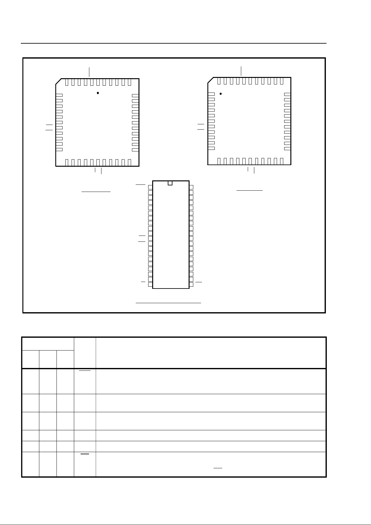
Figure 2 - Pin Connections
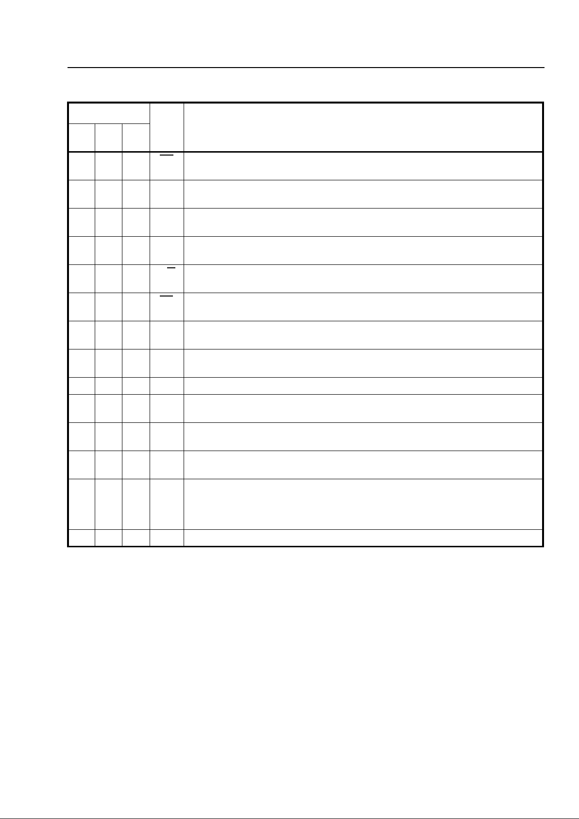
Pin Description
Pin #
Name Description
40
DIP44PLCC44QFP
1240DTAData Acknowledgemen t (Open Drai n Outpu t). This is the data a cknowledge men t
on the microprocessor interface. This pin is pulled low to signal that the chip has
processed the data. A 909 Ω, 1/4W, resistor is recommended to be used as a pullup.
2-4 3-5 41-43STi0-
STi2
ST-BUS Input 0 to 2 (Inputs). These are the inputs for the 2048 kbit/s ST-BUS input
streams.
571STi3ST-BUS Input 3 (Input). These are the inputs for the 2048 kbit/s ST-BUS input
streams.
6-9 8-11 2-5 IC Interna l Connecti on s. Must be connected to V
DD
.
10 12 6 V
DD
Power Input. Positive Supply .
11 13 7 F0i
Framing 0-Type (Input). This is the input for the frame synchronization pulse
for the 2048 kbit/s ST-BUS streams. A low on this input causes the internal counter
to reset on
the next negative transition of C4i.
1
65432
4443424140
7
8
9
10
11
12
13
14
15
16
39
38
37
36
35
34
33
32
31
30
23
1819202122
2425262728
17
29
STi3
IC
IC
IC
IC
VDD
F0i
C4i
A0
A1
A2
STo3
IC
IC
IC
IC
VSS
D0
D1
D2
D3
D4
NC
STi1
DTA
ODE
STo1
NC
NC
A4
DS
CS
D6
NC
A3
A5
R/W
D7
D5
44 PIN PLCC
DTA
STi0
STi1
STi2
STi3
IC
IC
IC
IC
VDD
F0i
C4i
A0
A1
A2
A3
A4
A5
DS
IC
ODE
STo0
STo1
STo2
STo3
IC
IC
IC
IC
VSS
D0
D1
D2
D3
D4
D5
D6
D7
CS
2
3
4
5
6
7
8
9
10
11
12
13
14
15
16
17
18
19
20
1
R/W
40
39
38
37
36
35
34
33
32
31
30
29
28
27
26
25
24
23
22
21
40 PIN CERDIP/PLASTIC DIP
STi2
STi0
IC
STo0
STo2
39
4443424140
3837363534
1
2
3
4
5
6
7
8
9
10
33
32
31
30
29
28
27
26
25
24
17
1213141516
1819202122
11
23
44 PIN QFP
STi3
IC
IC
IC
IC
VDD
F0i
C4i
A0
A1
A2
NC
A4
DS
CS
D6
NC
A3
A5
R/W
D7
D5
STo3
IC
IC
IC
IC
VSS
D0
D1
D2
D3
D4
NC
STi1
DTA
ODE
STo1
NC
STi2
STi0
IC
STo0
STo2

ISO-CMOS MT8981D
2-19
12 14 8 C4i 4. 096 MHz Clo ck (In put). ST-BUS bit cell boundaries lie on the alternate falling
edges of this clock.
13-1515-179-11 A0-A2 Address 0 to 2 (Inputs). These are the inputs for the addre ss lines on the
microprocessor interface.
16-1819-2113-15A3-A5 Address 3 to 5 (Inp uts). These are the inputs for the addre ss lines on the
microprocessor interface
19 22 16 DS Data Strobe (Inpu t). This is the input f or the active hig h data strobe on the
microprocessor interface.
20 23 17 R/W
Read or Write (Input). Th is is the input for the read/write signal on the
microprocessor interface - high for read, low for write.
21 24 18 CS
Chip Select (Inp ut). This is the input for the acti ve low chip select on the
microprocessor interface.
22-2425-2719-21D7-D5 Data 7 to 5 (Three-state I/O Pins). These are the bidirectional data pins on the
microprocessor interface.
25-2929-3323-27D4-D0 Data 4 to 0 (Three-state I/O Pins). These are the bidirectional data pins on the
microprocessor interface.
30 34 28 V
SS
Power Input. Negative Supply (Ground).
31-3435-3829-32IC Interna l Connec tions. Leave pins disconnected.
35 39 33 STo3 ST-BUS Output 3 (Three-state Outputs). These are the pins for the four 2048 kbit/s
ST-BUS output streams.
36-3841-4335-37STo2-
STo0
ST-BUS Output 2 to 0 (Three-state Outputs). These are the pins for the four 2048
kbit/s ST-BUS output streams.
39 44 38 ODE Output Drive Enabl e (In put). If this input is held high, the ST o0-STo3 output drivers
function normall y. If this input is low, the STo0-STo3 out put drivers go into thei r high
impedance state. NB: Even when ODE is high, channe ls on the STo 0-STo3 outputs
can go high impedance under software control.
40 1 39 IC Internal Connec tion. Leave pin disconnect e d.
Pin Description (continued)
Pin #
Name Description
40
DIP44PLCC44QFP

MT8981D ISO-CMOS
2-20
Functional Description
In recent years, there has been a trend in telephony
towards digital switching, particularly in association
with software control. Simultaneously, there has
been a trend in system architectures towards
distributed processing or multi-processor systems.
In accordance with these trends, MITEL has devised
the ST-BUS (Serial Telecom Bus). This bus
architectur e can be used both i n software-contr olled
digital voice and data switching, and for
interprocessor communications. The uses in
switching and in interprocessor communications are
completely integrated to allow for a simple general
purpose architecture appropriate for the systems of
the future.
The serial streams of the ST-BUS operate
continuously at 2048 kbit/s and are arranged in 125
µs wide frames which contain 32 8-bit channels.
MITEL manufactures a number of devices which
interface to the ST-BUS; a key device being the
MT8981 chip.
The MT8981 can switch data from channels on STBUS inputs to channels on ST-BUS outputs, and
simultaneously allows its controlling microprocessor
to read channels on ST-BUS inputs or write to
channels on ST-BUS outputs (Message Mode). To
the microprocessor, the MT8981 looks like a memory
peripheral. The microprocessor can write to the
MT8981 to establish switched connections between
input ST-BUS channels and output ST-BUS
channels, or to transmit messages on output STBUS channels. By reading from the MT8981, the
microprocessor can receive messages from ST-BUS
input channels or check which switched connections
have already been established.
By integrating both switching and interprocessor
communications, the MT8981 allows systems to use
distributed processing and to switch voice or data in
an ST-BUS architecture.
Hardware Descr iption
Serial data at 2048 kbit/s is received at the four STBUS inputs (STi0 to STi3), and serial data is
transmitted at the four ST-BUS outputs (STo0 to
STo3). Each serial input accepts 32 channels of
digital data, each channel containing an 8-bit word
which may represent a PCM-encoded analog/voice
sample as provided by a codec (e.g., MITEL’s
MT8964).
This serial input word is converted into parallel data
and stored in the 128 X 8 Data Memory. Locations in
the Data Memory are associated with particular
channels on particular ST-BUS input streams.
These locations can be read by the microprocessor
which controls the chip.
Locations in the Connection Memory, which is split
into high and low parts, are associated with
particular ST-BUS output streams. When a channel
is due to be transmitted on an ST-BUS output, the
data for the channel can either be switched from an
ST-BUS input or it can originate from the
microprocessor. If the data is switched from an
input, then the contents of the Connection Memory
Low location associated with the output channel is
used to address the Data Memory. This Data
Memory address corresponds to the channel on the
input ST-BUS stream on which the data for switching
arrived. If the data for the output channel originates
from the microprocessor (Message Mode), then the
contents of the Connection Memory Low location
associated with the output channel are output
directly, and this data is output repetitively on the
channel once every frame until the microprocessor
intervenes.
The Connection Memory data is received, via the
Control In terface, at D7 to D0. Th e Contr ol Interface
also receives address information at A5 to A0 and
handles the microprocessor control signals CS
,
DTA
, R/W and DS. There are two parts to any
address in the Data Memory or Connection
Memory. The higher order bits come from the
Figure 3 - Address Memory Map
A5 A4 A3 A2 A1 A0 H EX ADDRESS LOCATI ON
0
1
1
•
•
•
1
X
0
0
•
•
•
1
X
0
0
•
•
•
1
X
0
0
•
•
•
1
X
0
0
•
•
•
1
X
0
1
•
•
•
1
00 - 1F
20
21
•
•
•
3F
Control Register *
Channel 0
†
Channel 1
†
•
•
•
Channel 31
†
* Writing to the Control Register is the only fast transaction.
† Memory and stream are specified by the content s of the Control Regist er.

ISO-CMOS MT8981D
2-21
Control Register, which may be written to or read
from via the Control Interface. The lower order bits
come from the address lines directly.
The Control Register also allows the chip to
broadcast messages on all ST-BUS outputs (i.e., to
put every channel into Message Mode), or to split the
memory so that reads are from the Data Memory and
writes are to the Connection Memory Low. The
Connection Memory High determines whether
individual output channels are in Message Mode,
and allows individual output channels to go into a
high-impedance state, which enables arrays of
MT8981s to be constructed. It also controls the
CSTo pin.
All ST-BUS timing is derived from the two
signals C4i
and F0i.
Software Control
The address lines on the Control Interface give
access to the Control Regis ter directly or, depending
on the co ntents of the Control Regi ster, to the High
or Low sections of the Connection Memory or to the
Data Mem o ry.
If address line A5 is low, then the Control Register is
addressed regardless of the other address lines (see
Fig. 3). If A5 is high, then the address lines A4-A0
select the mem ory location corresponding to channel
0-31 for the memory and stream selected in the
Control Register.
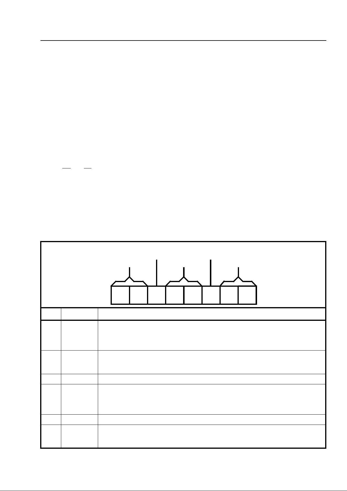
The data in the Control Register consists of mode
control bits, memory select bits, and stream address
bits (see Fig. 4). The memory select bits allow the
Connection Memory High or Low or the Data
Memory to be chosen, and the stream address bits
define one of the ST-BUS input or output streams.
Bit 7 of the Control Register allows split memory
operation - reads are from the Data Memory and
writes are to the Connection Memory Low.
The other mode control bit , bit 6, puts every output
channel on every output stream into active Message
Mode; i.e., the contents of the Connection Memory
Low are output on the ST-BUS output streams once
every frame unless the ODE pin is low. In this mode
the chip behaves as if bits 2 and 0 of every
Connection Memory High location were 1, regardless
of the actual valu es.
Figure 4 - Control Register Bits
BIT NAME DESCRIPTION
7 Split
Memory
When 1, all subsequent reads are from the Data Memory and writes are to the Connection
Memory Low, except when the Control Register is accessed again. When 0, the Memory
Select bits specify the memory for subsequent operati ons. I n either case, the Stream
Address Bits select the subsection of the memory which is made avail able.
6 Message
Mode
When 1, the contents of the Connection Mem or y Low are output on the Serial Output
streams except when the ODE pin is low. When 0, the Connection Memory bits for each
channel determine what is output.
5 (unused)
4-3 Memory
Select Bits
0-0 - Not to be used
0-1 - Data Memory (read only from the microprocessor port)
1-0 - Connection Memory Low
1-1 - Connection Memory High
2 (unused) Must be a 0.
1-0 Stream
Address
Bits
The number expressed in binary notation on these bit s refers to the input or outpu t STBUS stream which corresponds to the subsection of memory made accessible for
subsequent operations.
76 5432 10
Mode
Control
Bits
(unused) Memory
Select
Bits
Stream
Address
Bits
(unuse d)
 Loading...