MITEL MH89770N, MH89770S Datasheet
MH89770
T1/ESF Framer & Interface
Preliminary Information
Features
• Complet e interfac e to a bi direct iona l T1 link
• D3/D4 or ESF frami ng and S LC-96 com patib le
• Two frame elastic buffer with jitter tolerance
improved t o 156UI
• Insertion and dete ction of A, B, C, D bits
Signalling freeze , opt iona l debo unc e
• Selectable B8ZS, jammed bit (ZCS) or no zero
code suppression
• Yellow and blue al arm si gnal ca pabil ities
• Bipolar violation count, F
error count
• Frame and superframe sync. signals, Tx and Rx
• Per channel, overall, and remote loop around
• 8 kHz synchronization output
• Digital ph ase det ecto r betw een T1 line and
ST-BUS
• ST-BUS compatible
• Pin compatible with the MH89760BN/BS
• Inductorless clock recovery
• Loss of Sign al (LO S) indi cation
• Available in standard, narrow and surface
mount form ats
error count, CRC
T
ISSUE 2 March 1995
Ordering Information
MH89770N 40 Pin DIL Hybrid 0.8" row pitch
MH89770S 40 Pin Surface Mount Hybrid
0°C to 70°C
Applications
• DS1/ESF di gital trun k in terface s
• Computer to PBX interfaces (DMI and CPI)
• High speed computer to computer data links
Description
The MH89770 is a complete T1 interface solution,
meeting the Extended Super Frame (ESF), D3/D4
and SLC-96 formats. The MH89770 interfaces to the
DS1 1.544 Mbit/sec digital trunk and has the
capability of meeting ACCUNET
tole ran c e (13 8 UI ).
The MH89770 is a pin-compatible enhancement of
the MH89760B.
®1
T1.5 wander
TxSF
C2i
F0i
RxSF
DSTo
DSTi
CSTi0
CSTi1
CSTo
VDD
XCtl
XSt
ST-BUS
Timing
Circuitry
Data
Interface
Serial
Control
Interface
Control
Logic
1. ACCUNET® T1.5 is a registered trademark of AT & T.
Two Frame
Elastic
Buffer with
Slip Contro l
DS1
LINK
INTERFACE
2048 - 1544
Converte r
ABCD
Signalling RAM
Phase
Detector
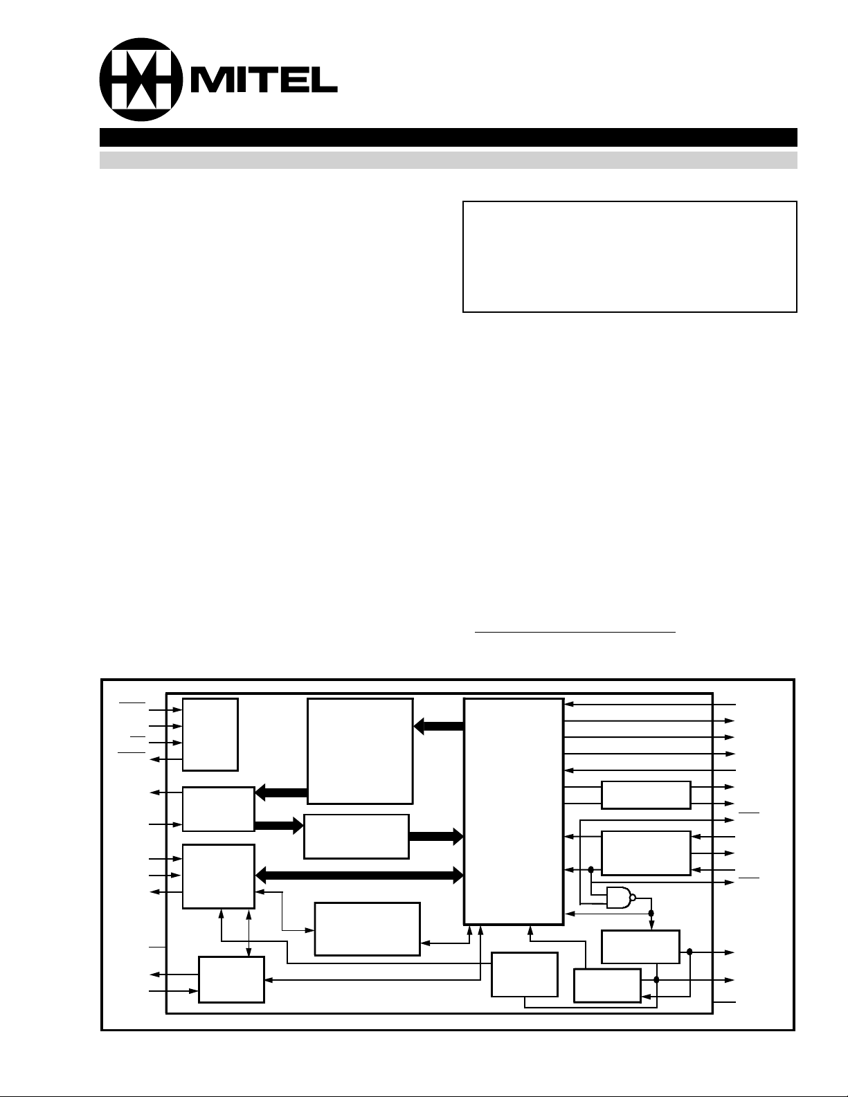
Figure 1 - Functional Block Diagram
DS1
Counter
Transmit ter
Receiver
Clock
Extractor
C1.5i
RxFDLClk
RxFDL
TxFDLClk
TxFDL
OUTA
OUTB
RxA
RxT
LOS
RxR
RxB
E1.5o
E8Ko
VSS
4-125
MH89770 Preliminary Information
40
NC
39
38
37
36
35
34
33
32
31
30
29
28
27
26
25
24
23
22
21
NC
LOS
NC
TxFDL
NC
TxFDLClk
VSS
RxFDLClk
DSTo
RxFDL
OUTB
C1.5i
RxSF
TxSF
OUTA
NC
NC
NC
VSS
Pin Description
2
NC
NC
XSt
NC
C2i
F0i
3
4
5
6
7
8
9
10
11
12
13
14
15
16
17
18
19
20
E1.5o
VDD
RxA
RxT
RxR
RxB
CSTi1
CSTi0
E8Ko
XCtl
CSTo
DSTi
E1.5o
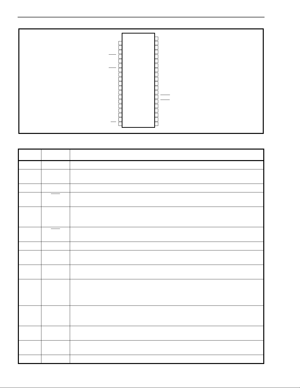
Figure 2 - Pin Connections
Pin # Name Description
2NCNo Connection.
3E1.5o1.544 MHz Extracted Cl ock (Output): Thi s clock is extra cted by the device from the
received DS1 signal. It is used internally to clock in data received at RxT and RxR.
4V
DD
5RxA
System Power Supply. +5V.
Received A (Output): The bipolar DS1 signal received by the device at RxR and RxT is
converted to a unipolar format and output at this pin.
6
7
RxT
RxR
Receive Tip and Ring Inputs: Bipolar split phase inputs designed to be connected
directly to the input transformer. I mpe dance to ground is approximately 1kΩ.
Impedance between pins=430Ω.
8RxB
Received B (Output): The bipolar DS1 signal received by the device at RxR and RxT is
converted to a unipolar format and output at this pin.
9NCNo Connection.
10 CSTi1 Control ST-BUS Input #1: A 2048 kbit/s serial control stream which carries 24
per-channel control words.
11 CSTi0 Control ST-BUS Input #0: A 2048 kbit/s serial control stream that contain s 24 per
channel control words and two master control words.
12 E8Ko 8 kHz Extracted Clock (Output): This is an 8 kHz output generated by dividing the
extracted 1.544 MHz clock by 193 and aligning it with the received DS1 frame. The 8
kHz signal can be used for synchronizing system clocks to the extracted 1.544 MHz
clock. When digital loopback is enabled, the 8kHz is derived from C1.5.
13 XCtl External Control (O utpu t ): This is an uncommitt ed external outpu t pin which is set or
reset via bit 3 in Master Control Word 1 on CSTi0. The state of XCtl is updated once per
frame.
14 XSt External Status (Sch mitt Trigger Input ): The state of this pin is sampled once per
frame and the status is reporte d in bit 5 of Master Status Word 2 on CSTo.
15 CSTo Control ST-BUS Output: This is a 2048 kbit/s serial control stream which provides the
24 per-channel status words, and two master statu s words.
16 NC No Con nec tion .
4-126
Preliminary Information MH89770
Pin Description (Continued)
Pin # Name Description
17 DSTi Data ST-BUS Input: This pin accepts a 2048 kbit/s serial stream which contains the 24
PCM or data channels to be transmit ted on the T1 trunk.
18 C2i 2.0 48 MHz Sy stem Clock (Inp ut ): This is the master clo c k for the ST-BUS section of
the chip. All data on the ST-BUS is clocked in on the falling edge of C2i and out on the
rising edge.
19 E1.5o 1.544 MHz Ex tracted Cl ock (Ou tput): Internal ly connected to Pin 3.
20 F0i
Frame Pulse Input: This is the frame synchronizati on signal which def ines the
beginning of the 32 channel ST-BUS frame.
21 V
SS
System ground.
22-24 NC No Con nec tion .
25 OUTA Output A (Open Collector Output): This is the output of the DS1 transmitter circuit. It is
suitable for use with an external pulse transformer to generate the transm it bipolar line
signal.
26 TxSF
Transmit Superfram e Pulse Inp ut: A low pulse applied at this pin will determ ine the
start of the next transmit superframe as illustrated in Figure 20. The device will free run if
this pin is held high.
27 RxSF
Received Superframe Pulse Output: A pulse output on this pin indicates that the next
frame of data on the ST-BUS is from frame 1 of the received superframe. The period is
12 frames long in D3/D4 modes and 24 frames in ESF mode. Active only when device is
synchronized to received DS1 signal.
28 C1.5i 1.544 MHz Clock Inpu t: The rising edge of this clock is used to output data on OUTA,
OUTB. C1.5i must be pha se -lo c ked to the C2i system cl o c k.
29 OUTB Output B (Open Collector Output): This is the output of the DS1 transmitter circuit. It is
suitable for use with an external pulse transformer to generate the transm it bipolar line
signal.
30 RxFDL Received Facility Data Link (Output): A 4 kbit/s serial output stream that is
demultiple xed from the FDL bits in ESF mode, or the received F
bit pattern when in
S
SLC96 mode. It is clocked out on the rising edge of RxFDLClk.
31 DSTo Data ST-BUS Output: A 2048 kbit/s serial output stream which contains the 24 PCM or
data channels received from the DS1 line.
32 RxFDLClk Receive Facility Data Link Cl ock Ou tput: A 4 kHz clock used to output FDL
information on RxF DL. Data is clocked out on the rising edge of the clock.
33 V
SS
No Connection.
34 TxFDLCl k Transmit Facility Data Link Clock Outp ut: A 4 kHz clock used to input FDL
information on TxFDL. Data is cloc ked in on the rising edge of the clock.
35 NC No Con nec tion .
36 TxFDL Transmit Facility Data Link (Input)
FDL bits in the ESF mode, or the F
: A 4 kbit/s serial input stream that is muxed into the
pattern when in SLC96 mode. It is clocked in on the
S
rising edge of TxFDLClk.
37 NC No Con nec tion .
38 LOS Loss of Signal (Output): This pin goes high when 128 contiguous ZEROs are received
on the RxT and RxR inputs. When LOS is high, RxA
and RxB are forced high. LOS is
reset when 48 ones are received in a two T1-frame period.
39 NC No Con nec tion .
40 NC No Connection.
4-127
MH89770 Preliminary Information
X
31
MC
W2
31
31
MS
W2
29 30 31
25 26 27 28
21 22 23 24
17 18 19 20
13 14 15 16
9 101112
X
X
X
X
X
X
1
30
PC
CW
1
29
28
26
25
24
22
21
20
18
17
16
14
13
12
10
9
8
15
PC
PC
27
PC
PC
PC
23
PC
PC
PC
19
PC
PC
PC
PC
PC
PC
11
PC
PC
PC
7
CW
CW
X
CW
CW
CW
X
CW
CW
CW
X
CW
CW
CW
MC
CW
CW
CW
X
CW
CW
CW
X
1
1
1
1
1
1
1
1
1
1
W1
1
1
1
1
1
1
29 30 31
X
25 26 27 28
X
21 22 23 24
X
17 18 19 20
X
13 14 15 16
X
9101112
ST-BUS CHANNE L VERSUS DS1 CHANNEL TRANSMITTED
X
ST-BUS CHANNEL V ERSUS DS1 CHANNEL RECEIVED
30
29
28
26
25
24
22
21
20
18
17
16
14
13
12
10
9
ST-BUS CHANNEL VERSUS DS1 CHANNEL CONTROLLED
8
PC
PC
PC
27
PC
PC
PC
23
PC
PC
PC
19
PC
PC
PC
15
PC
PC
PC
11
PC
PC
PC
7
CW
CW
CW
X
CW
CW
CW
X
CW
CW
CW
X
CW
CW
CW
X
CW
CW
CW
X
CW
CW
CW
X
2
2
2
2
2
2
2
2
2
2
2
2
2
2
2
2
2
2
ST-BUS CHANNEL VERSUS DS1 CHANNEL CONTROLLED
15
30
29
28
26
25
24
22
21
20
18
17
16
14
13
12
10
9
8
27
23
19
MS
11
7
PCS
PCS
PCS
X
PCS
PCS
PCS
X
PCS
PCS
PCS
X
PCS
PCS
PCS
W1
PCS
PCS
PCS
X
PCS
PCS
PCS
X
W
W
W
W
W
W
W
W
W
W
W
W
W
W
W
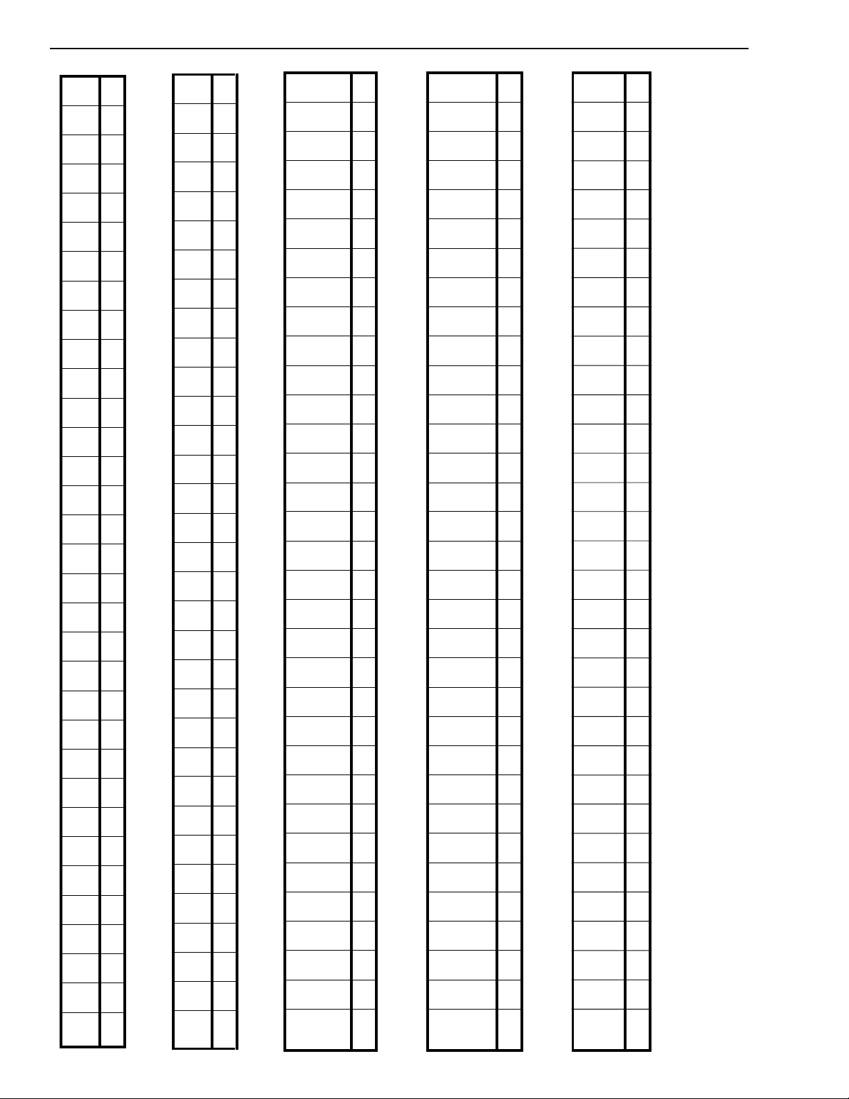
Figure 3 - ST-BUS Channel Allocations
W
W
W
ST-BUS VERSUS DS1 CHANNEL STATUS
5678
X
1234
X
DSTi 0
DS1 1 2 3 4 5 6 7 8 9 10 11 12 13 14 15 16 17 18 19 20 21 22 23 24
4-128
5678
X
1234
X
DSTo 0
DS1 1 2 3 4 5 6 7 8 9 10 11 12 13 14 15 16 17 18 19 20 21 22 23 24
6
1
PC
CW
5
1
PC
CW
4
1
PC
CW
3
X
2
1
PC
CW
1
1
PC
CW
1
PC
CW
CSTi0 0
DS1 1 2 3 4 5 6 7 8 9 10 11 12 13 14 15 16 17 18 19 20 21 22 23 24
PCCW=Per Channe l C on tr o l Wo r d, MCW1/2=Mas ter Control W o rd 1/2
6
5
4
2
1
0
CSTi1
PC
PC
PC
3
PC
PC
PC
CW
CW
CW
X
CW
CW
CW
2
2
2
2
2
2
DS1 1 2 3 4 5 6 7 8 9 10 11 12 13 14 15 16 17 18 19 20 21 22 23 24
PCCW=Per Channe l C on tr o l Wo r d
6
PCS
5
PCS
4
PCS
3PSW
2
PCS
1
PCS
PCS
CSTo 0
W
W
W
W
W
W
DS1 1 2 3 4 5 6 7 8 9 10 11 12 13 14 15 16 17 18 19 20 21 22 23 24
PCSW=Per Channel Status Word, PSW=Phase Status Word, MSW=Master Status Word
X = UNUSED

Preliminary Information MH89770
Functional Description
The MH89770 is a thick film hybrid solution for a T1
interface. All of the formatting and signalling
insertion and detection is done by the device.
Various programmable options in the device include:
ESF, D3/D4 or SLC-96 mode, common channel or
robbed bit signalling, zero code suppression, alarms,
and local and remote loopback. The MH89770 also
has built in bipolar line drivers and receivers and a
clock extraction circuit.
All data and control information is communicated to
the MH89770 via 2048 kbit/s serial streams
conforming to Mitel’s ST-BUS format.
The ST-BUS is a TDM serial bus that operates at
2048 kbits/s. The serial streams are divided into 125
µsec frames that are made up of 32 8-bit channels. A
serial stream that is made up of these 32 8 bit
channels is known as an ST-BUS stream, and one of
these 64 kbit/s channels is known as an ST-BUS
channel.
The system side of the MH89770 is made up of
ST-BUS inputs and outputs, i.e., control inputs and
outputs (CSTi/o) and data inputs and outputs
(DSTi/ o). These signals are functionally represented
in Figure 32. The DS1 line side of the device is made
up of split phase inputs (RxT, RxR) and outputs
(OUTA, OUTB) which can be connected to line
coupling transformers. Functional transmit and
receive timing is shown in Figures 33 and 34.
Data for transmission on the DS1 line is clocked
serially into the device at the DSTi pin. The DSTi pin
accepts a 32 channel time division multiplexed
ST-BUS stream. Data is clocked in with the falling
edge of the C2i clock. ST-BUS frame boundaries are
defined by the frame pulse applied at the F0i
Only 24 of the available 32 c hannels on the ST-BUS
serial stream are actually transmitted on the DS1
side. The unused 8 channels are ignored by the
device.
Data recei ved from the DS1 l ine is clocked out of th e
device in a similar manner at the DSTo pin. Data is
clocked out on the rising edge of the C2i clock. Only
24 of the 32 channels output by the device contain
the information from the DS1 line. The DSTo pin is,
however, actively driven during the unused channel
timeslots. Figure 3 shows the correspondence
between the DS1 channels and the ST-BUS
channels.
All control and monitoring of the device is
accomplished through two ST-BUS serial control
pin.
inputs and one ser ial control outpu t. Control ST-BUS
input number 0 (CSTi0) accepts an ST-BUS serial
stream which contains the 24 per channel control
words and two master control words. The per channel
control words relate directly to the 24 information
channels output on the DS1 side. The master control
words affect operation of the whole device. Control
ST-B US input n umber 1 (CSTi1) accepts an ST-BUS
stream containing the A, B, C and D signalling bits.
The relationship between the CSTi channels and the
controlled DS0 channels is shown in Figure 3. Status
and signalling information is received from the device
via the control ST-BUS output (CSTo). This serial
outpu t stream contain s two m aster st atus wo rds, 24
per channel status words and one Phase Status
Word. Figure 3 shows the correspondence between
the received DS1 channels and the status words.
Detailed information on the operation of the control
interface is presented be low.
Programmable Features
The main features in the device are programmed
through two master control words which occupy
channels 15 and 31 in Control ST-BUS input stream
number 0 (CSTi0). These two eight bit words are
used to:
• Select the di fferent operati ng mo de s of the
device ESF, D3/D4 or SLC-96.
• Activate th e fea tures th at are n ee ded in a
certain application; common channel signalling,
zero code s uppressi on , signal ling d eboun ce,
etc.
• Turn on in service alarm s, d iagno stic lo op
arounds, and the ext erna l cont rol funct ion
Tables 1 and 2 contain a complete explanation of the
function of the different bits in Master Control Words
1 and 2.
Major Operating Modes
The major operating modes of the device are
enabled by bits 2 and 4 of Master Control Word 2.
The Extended Superframe (ESF) mode is enabled
when bit 4 is set high. Bit 2 has no effect in this
mode. The ESF mode enables the t ransmission of
the S bit pattern shown in Table 3. This includes the
frame/superframe pattern, the CRC-6, and the
Facility Data Link (FDL). The device generates the
frame/multiframe pattern and calculates the CRC for
each superframe. The data clocked into the device
on the TxFDL pin is incorporated into the FDL. ESF
mode will also ins e rt A, B, C and D si gnalling bits into
the 24 f rame multiframe. The DS1 frame begins after
4-129

MH89770 Preliminary Information
Bit Name Description
7 Debounce When set the received A, B, C and D signalling bits are reported directly in the per
channel status words output at CSTo. When clear, the signalling bits are debounced for 6
to 9 ms before they are placed on CSTo.
6 TSPZCS Transparent Zero Code Suppression. When this bit is set, no zero code suppression is
implemented.
5 B8ZS Binary E ight Zero Suppr essi on . When this bit is set, B8ZS zero code suppression is
enabled. When clea r, bit 7 in data channels containing all zeros is for ced high before
being transmitted on the DS1 side. This bit is inactive if the TSPZ CS bit is set.
4 8kHSel 8 kHz Output Select. Whe n set, the E8Ko pin is held hig h. When clear, the E8Ko
generates an 8 kHz output derived from the extracted 1.544 MH z clock or C1.5i clock
(see Pin Description for E8Ko).
3 XCtl External Control Pin. When set, the XCtl pin is held high. Whe n clear, XCtl is held low.
2 ESFYLW ESF Yellow Alarm. Valid only in ESF mode. When set, a sequence of eight 1’s followed
by eight 0’s is sent in the FDL bit positions. When clear , the FDL bit contains data input at
the TxFDL pin.
1 Robbed bit When this bit is set, robbed bit signalling is disabled on all DS0 transmit channels. When
clear, A, B, C and D signalling bits are inserted into bit position 8 of all DS0 channels in
every 6th frame.
0 YLALR Yellow Alarm. When set, bit 2 of all DS0 channels is set low. When clear, bit 2 operates
normally.
Table 1. Master Control Word 1 (Channel 15, CSTi0)
.
Bit Na me Description
7 RMLOOP Remote Loopback. When set, the data received at RxR and RxT is looped back to OUTB
and OUTA respectively. The data is clocked into the device with the extracted 1.544 MHz
clock. The device still monit ors the received dat a and outpu ts it at DSTo. The device
operates normally when the bit is clear.
6 DGLOOP Digital Loop back . When set, the data input on DSTi is looped around to DSTo. The
normal received data on RxR and RxT is ignored. However, t he dat a input at DSTi is still
transmitted on OUTA and OUTB. The device frames up on the looped data using the C1.5i
clock.
5 ALL1'S All One’s Alarm. When set, the chip tra nsmit s an unfram ed all 1's signal on OUTA and
OUTB.
4 ESF/D4 ESF/D4 Select. When set, the device is in ESF mode. When clear, the device is in D3/D4
mode.
3 ReFR Reframe. If set for at least one frame and then cleared, the chip will begi n to sea rch for a
new frame position. Only th e change from high to low will cause a reframe, not a
continuous low level.
2 S LC -96 SLC-96 Mode Select. The chip is in SLC-96 mode when this bit is set. This enables input
and output of the F
bit pattern using the same pins as the facilit y data link in ESF mode .
S
The chip will use the same framing algorithm as D3/D4 mod e. The user must insert the
valid F
bits in 2 out of 6 superframes to allow the receiver to find superframe sync, and
S
the transmitter to insert A and B bits in every 6th frame. The SLC-96 FDL completely
replaces the F
pattern in the outgoing S bit positi on. Inacti ve in ES F mode.
S
1 CRC/MIM IC In ESF mode, when set, the chip disregards the CRC calculat ion durin g synchronization .
When clear, the device will check for a correct CRC before going into synchronization. In
D3/D4 mode, when set, the device will synchronize on the first correct S-bit pattern
detected. When this bit is clear , the device will not synchronize if it has detected more than
one candidate for the frame alignm ent pat te rn (i.e., a mimic ).
0 Maint. M ain tenan ce Mode . When set, the device will declare itself out-of-sync if 4 out of 12
consecutive F
bits. In this mode, four consecutive bits following an errored F
bits are in error. When clear, the out-of-sync threshold is 2 errors in 4 FT
T
bit are examined.
T
Table 2. Master Control Word 2 (Channel 31, CSTi0)
4-130
Preliminary Information MH89770
approximately 25 periods of the C1.5i clock from the
F0i
frame pulse.
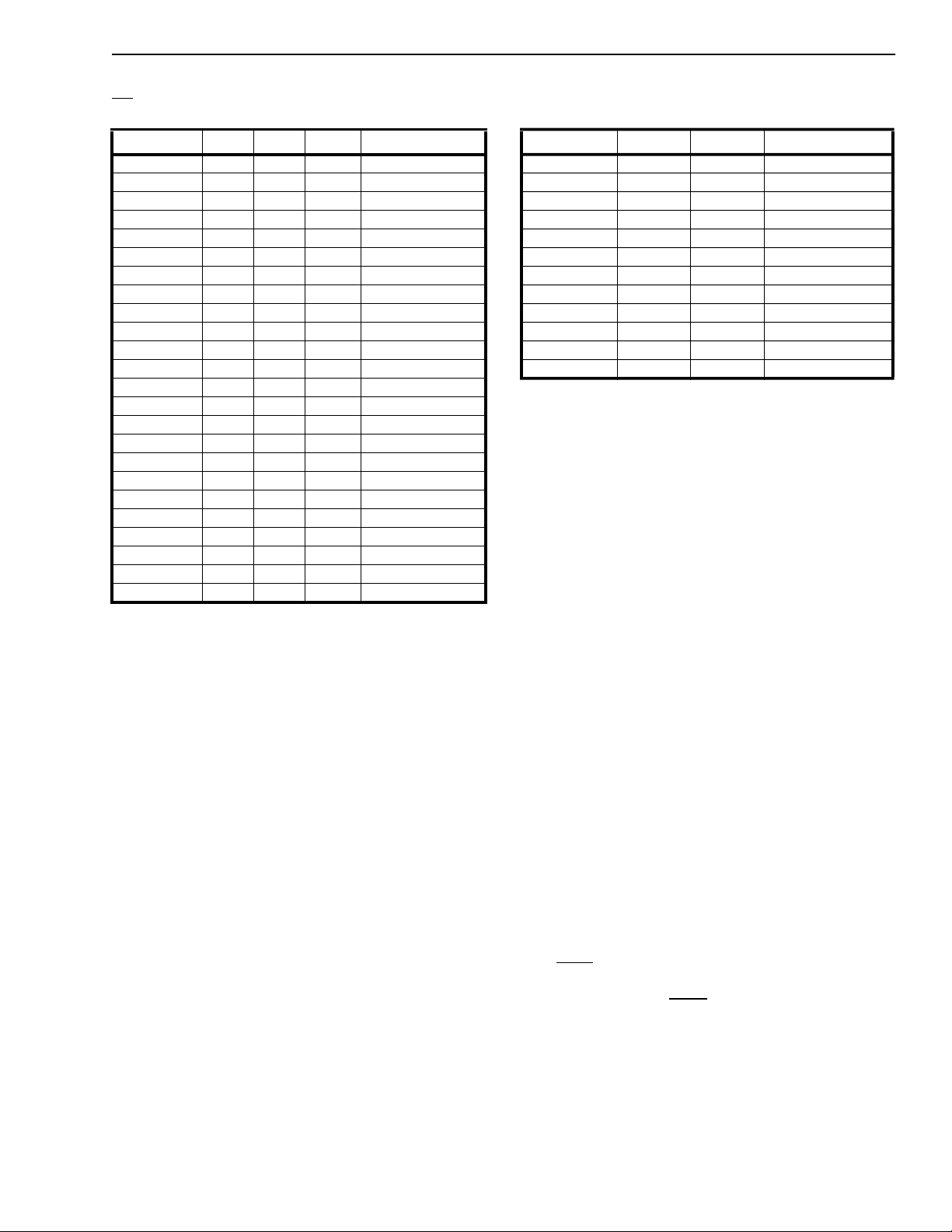
Frame # F PS FDL CRC Signalling
†
1X
2CB1
3X
40
5X
6CB2A
7X
80
9X
10 CB3
11 X
12 1 B
13 X
14 CB4
15 X
16 0
17 X
18 CB5 C
19 X
20 1
21 X
22 CB6
23 X
24 1 D
Table 3. ESF Fra me Pat ter n
† These signalling bits are only valid if the robbed bit signal ling is
active.
‡
During synchronization the receiver locks on to the
incoming frame, calculates the CRC and compares it
to the CRC received in the next multiframe. The
device will not declare itself to be in synchronization unless a valid framing pattern in the S-bit is
detected and a correct CRC is received. The CRC
check in this case provides protection against false
framing. The CRC check can be turned off by setting
bit 1 in Master Control Word 2.
The device can be forced to resynchronize itself. If
Bit 3 in Master Cont rol Word 2 is set for one frame
and then subsequently reset, the de vice will start to
search for a new frame position. The decision to
reframe is made by the user’s system processor on
the basis of the status conditions detected in the
received master status words. This may include
consideration of the number of errors in the received
CRC in conjunction with an indication of the
presence of a mimic. When the device attains
synchronization the mimic bit in M aster Status Word
1 is set if the device found another possible
candidate when it was searching for the framing
pattern.
FPS) exceed the threshold set with bit 0 in Master
Control Wor d 2.
Frame # F
T
F
S
Signalling
†
11
20
30
40
51
61A
70
81
91
10 1
11 0
12 0 B
Table 4. D3/D4 Framer
† These signalling bits are only valid if the robbed bit signalling is
active.
Standard D3/D4 framing is enabled when bit 4 of
Master Control Word 2 is reset (logic 0). In this mode
the device searches for and inserts the framing
pattern shown in Table 4. This mode only supports
AB bit signalling, and does not contain a CRC check.
The CRC/MIMIC bit in Master Control Word 2, when
set high, allows the device to synchronize in the
presence of a mimic. If this bit is reset, the device will
not synchronize in the presence of a mimic. (Also
refer t o section on Framing Algorithm.)
In the D3/D4 mode the device can also be made
compatible with SLC-96 by setting bit two of Master
Control Word 2. This allows the user to insert and
extract the signalling framing pattern on the DS1 bit
stream using the FDL input and output pins. The
user must format this 4 kbits of information externally
to meet all of the requirements of the SLC-96
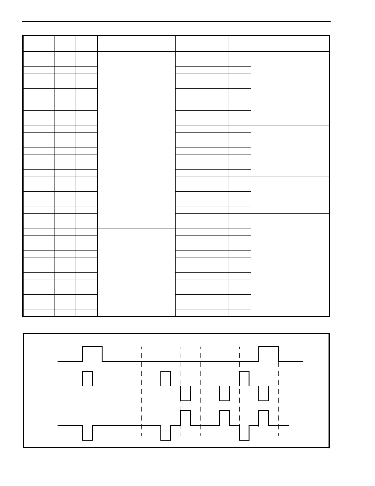
specification (see Table 5). The device multiplexes
and demultiplexes this information into the proper
position. This mode of operat ion can also be used for
any other application that uses all or part of the
signalling framing pattern. As long as the serial
stream clocked into the TxFDL contains two proper
sets of consecutive synchronization bits (as shown in
Table 5 for fr am es 1 to 2 4) , the device will be
able to insert and extract the A, B signalling bits.
The TxSF
pin should be held high in this mode.
Superframe boundaries cannot be defined by a pulse
on this inp ut. The RxSF
output functions normally
and indicates the superframe boundaries based on
the synchronization pattern in the F
received bit
S
position.
Note that the devi ce wi ll resync hroniz e auto mati cally
if the errors in the terminal framing pattern (F
T
or
4-131
MH89770 Preliminary Information
Frame
#
F
T
11
†
F
S
Notes
Frame
#
37 1
F
T
†
F
S
20 38X
30 390
40 40X
51 411
60 42X
70 430
81 44X
91 451
10 1 46 X
11 0 47 0
12 1 48 S
13 1 49 1
14 0 50 S
Resynchronization
Data
Bits
15 0 51 0
16 0 52 S
17 1 53 1
18 0 54 C
19 0 55 0
20 1 56 C
21 1 57 1
22 1 58 C
23 0 59 0
24 1 60 A
25 1
61 1
26 X 62 A
27 0 63 0
28 X 64 L
29 1 65 1
30 X 66 L
31 0 67 0
X =Concentrator
Fiel d Bi ts
32 X 68 L
33 1 69 1
34 X 70 L
35 0 71 0
36 X 72 S
Tab le 5. S LC-96 Fram ing P attern
† Note: The FS pattern has to be supplied by the user.
Notes
X = Concentrator
Field B i ts
S = Spoiler Bits
C = Maintenance
Field
Bits
A = Alarm Field
Bits
L = Line S wi tc h
Field B i ts
S = Spoiler Bits
4-132
DATA
B8ZS
B8ZS
B0 00V
B
000
B
V
B
Figure 4 - B8ZS Output Coding
0
V
V
0
B
B
B
B
V = Violation
B = Bipolar
0 = No Pulse

Preliminary Information MH89770
Zero Code Suppression
The combination of bits 5 and 6 in Master Control
Word 1 allow one of three zero code suppression
schemes to be selected. The three choices are:
none, binary 8 zero suppression (B8ZS), or jammed
bit (bit 7 forced high). No zero code suppression
allows the device to interface with systems that have
already applied some form of zero code suppression
to the data input on DSTi. B8ZS zero code
suppression replaces all strings of 8 zeros with a
known bit pattern and a specific pattern of bipolar
violations. This bit pattern and violation pattern is
shown in Figure 4. The receiver monitors the
received bit pattern and the bipolar violation pattern
and replaces all matching strings wit h 8 zeros.
Loopback Modes
Remote and digital loopback modes are enabled by
bits 6 and 7 in Master Cont rol Word 2. These modes
can be used for diagnostics in locating the source of
a fault condition. Remote loop around loops back
data received at RxR and RxT back out on OUTA
and OUTB, thus effectively sending the received
DS1 data back to the far end unaltered so that the
transmission line can be tested. The received signal
with the appropriate received channels on the DS1
side made available in the proper format at DSTo.
The digital loop around mode diverts the data
received at DSTi back out the DSTo pin. Data
received on DSTi is, however, still t ransmitted out via
OUTA and OUTB. This loop back mode can be used
to test the near end interface equipment when there
is no transmission line or when there is a suspected
fail ure of th e line .
The all ones transmit alarm (also known as the blue
alarm or the keep alive signal) can be activated in
conjunction with the digital loop around so that the
transmission line sends an all 1's signal while the
normal data is looped back locally.
The MH89770 also has a per channel loopback
mode. See Table 6 and the following section for more
information.
Per Channel Control Feature s
In addition to the two master control words in CSTi0
there are also 24 Per Channel Control Words. These
control words only affect individual DS0 channels.
The correspondence between the channels on
CSTi0 and the affected DS0 channel is shown in
Fig. 3. Each control word has three bits that enable
robbed bit signalling, DS0 channel loopback and
inversion of the DS0 channel. A full description of
each of the bits is provided in Table 6.
Transmit Signalling Bits
Control ST-BUS input number 1 (CSTi1) contains 24
additional per channel control words. These 24
ST-BUS channels contain the A, B, C and D
signalling bits that the device uses at transmit time.
The position of these 24 per channel control words in
the ST-BUS is
the ABCD signalling bits is shown in Table 7. Even
though the device only inserts the signalling
shown in Figure 3 and the position of
Bit Name Description
7-3 IC Internal Connections. Must be kept at 0 for normal operation.
2 Polarity When set, the applicable channel is not inverted on the transmit or the receive side of
the device. When clear, all the bits within the applicable channel are inverted both on
transmit and receive side.
1 Loop Per C ha nne l Loop back. When set, the received DS0 channel is replaced with the
transmitted DS0 channel. Only one DS0 channel may be looped back in this manner at
a time. The transmitted DS0 channel remains unaffected. When cl ear the transmi t and
receive DS0 sections operate normally.
0 Data Data Channel Enable. When set, robbed bit signalli ng for th e applicabl e channel is
disabled. When clear, every 6th DS1 frame is available for robbed bit signalling. This
feature is enabled only if bit 1 in Master Control Word is low.
Table 6. Per Channel Control Word 1 Input at CSTi0
Bit Name Descri ptio n
7-4 Unuse d Keep at 0 for normal operation
3
2
1-0
A
B
C, D
These are the 4 signalling bits inserted in the appropriate channels of the DS1 stream
being output from the chip, when in ESF mode. In D3/D4 modes where there are only
two signalling bits, the values of C and D are ignored.
Table 7. Per Channel Control Word 2 Input at CSTi1
4-133
MH89770 Preliminary Information
Bit Name Description
7 YL ALR Yellow Alarm In dicatio n. This bit is set when the chip is receiving a 0 in bit position 2
of every DS0 channel.
6MIMICThis bit is set if the frame search algorithm found more than one possible frame
candidate when it went into frame synchronization.
5 ERR Term i na l Fram ing Bit Error. The state of this bit changes every time the chip detects
4 errors in the F
96ms.
4 ESF YLW ESF Yellow Alarm. This bit is set when the device has observed a sequence of eight
one’s and eight 0’s in the FDL bit positions.
3MFSYNC
Multiframe Synchronization. This bit is cleared when D3/D4 multifram e
synchronization has been achieved. Applicable only in D3/D4 and SLC-96 modes of
operation.
2 BPV Bipolar Violation Count. The state of this bit changes every time the device counts
256 bipolar violations.
1 SLIP Slip In di cation. This bit changes state every time the elastic buffer in the device
performs a controlled slip.
0 SYN
Synchronizatio n. This bit is set when the device has not achieved synchronizat ion.
The bit is clear when the device has synchronized to the received DS1 data stream.
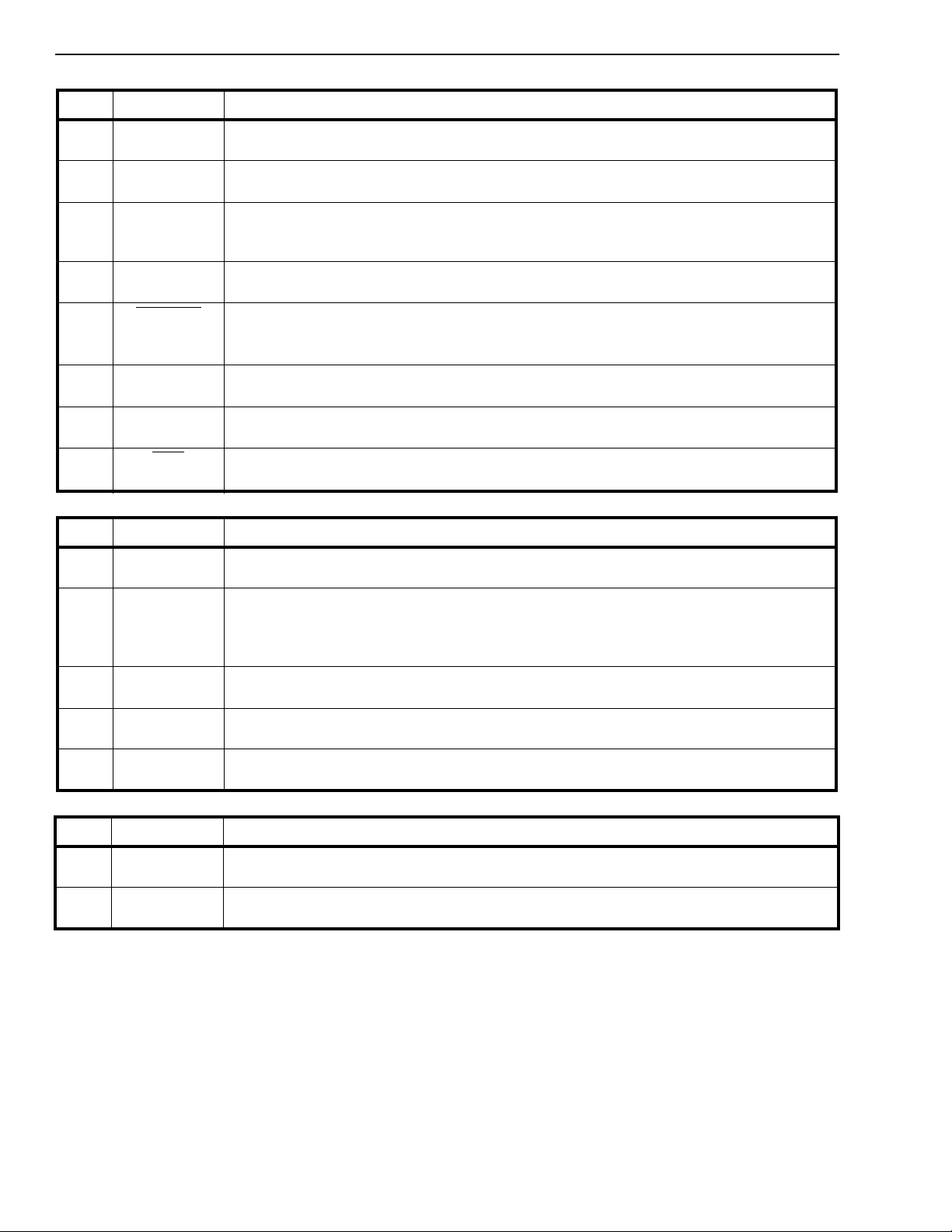
Tab le 8 . Master Statu s Word 1 (Chan nel 15 , CSTo)
or FPS bit pattern. The bit will not change state more than once every
T
.
Bit Name Description
7 BlAlm Bl ue Al arm . This bit is set if the receiver has detected two frames of 1’s and an out of
frame condition. It is reset by any 250 microsecond interval that contain s a zero.
6 FrCn t Frame Count. This is the ninth and most signifi cant bit of the “Phase Stat us Word”
(see Table 10). If the phase status word is increment ing, this bit will toggle when th e
phase reading ex ceeds channel 31, bit 7. If the phase word is decrementing, then this
bit will toggle when the reading goes below channel 0, bit 0.
5 XSt External Status. This bit reflects the state of the external status pin (XSt). The state of
the XSt pin is sampled once per frame.
4-3 BPVCnt Bipolar Violation Count. These two bits change state every 128 and every 64 bipolar
violations, respectively.
2-0 CRCCNT CRC Error Count. These three bits count received CRC errors. The counter will reset
to zero when it reaches terminal count. Valid only in ESF mode.
Tab le 9 . Master Statu s Word 2 (Chan nel 31 , CSTo)
Bit Name Descri ptio n
7-3 ChannelCnt Channel Count. These five bits indicate the ST-BUS channel count between the
ST-BUS frame pulse and the rising edge of E8Ko.
2-0 BitCnt Bit Cou nt. These three bits provide one bit resolutio n within the channel count
described above.
Table 10. Phase Status Word (Channel 3, CSTo)
information in every 6th DS1 frame this information
Operating Status Information
must be input every S T-BUS frame.
Status Information regarding the operation of the
Robbed bit signalling can be disabled for all
channels on the DS1 link by bit 1 of Master Control
Word 1. It can also be disabled on a per channel
basis by bit 0 in the Per Channel Control Word 1.
device is output serially via the Control ST-BUS
output (CSTo). The CSTo serial stream contains
Master Status Words 1 and 2, 24 Per Channel Status
Words, and a Pha se Status Word . The Ma ster Statu s
Words contain all of the information needed to
determine the state of the interface and how well it is
operating. The information provided includes frame
and super frame synchronization, slip, bipolar
4-134

Preliminary Information MH89770
Bit Name Description
7-4 Unused Unused Bits. Will be output as 0’s.
3
2
1
0
A
B
C
These are the 4 signalling bits as extracted from the received DS1 bit stream.
The bits are debounced for 6 to 9 ms if the debounce feature is enabled via bit 7 in
Master Control Word 1.
D
Table 11. Per Channel Status Word Output on CSTo
.
violation counter, alarms, CRC error count, FT error
count, synchronization pattern mimic and a phase
status word. Tables 8 and 9 give a description of each
of the bits in Master Status Words 1 and 2, and Table
10 gives a des crip t ion of the Phase Status Wor d.
In addition, the MH89770 has a Loss of Signal (LOS)
pin that is set High when 128 conse cutive ZER O s are
received. While LOS is set High, RxA
and RxB are
forced High. The LOS signal goes Low when a ONEs
density on 12.5% of the bits (equivalent to 48 bits)
occurs in a two DS1 frame period.
Alarm Detect ion
The device detects the yellow alarm for both D3/D4
frame format and ESF format. The D3/D4 yellow
alarm will be activated if a ‘0’ is received in bit
position 2 of every DS0 channel for 600 msec. It will
be released in 200 msec after t he content s of the bit
change. The alarm is detectable in the presence of
errors on the line. The ESF yellow alarm will become
active when the device has detected a string of eight
0’s followed b y eight 1’s i n the facili ty data link. It is
not detectable in the presence of errors on the line.
This means that the ESF yellow alarm will drop out
for rela tive ly short p er iod s o f time, s o t he s y stem will
have to integrate the ESF yellow alarm. The blue
alarm signal, in Master Status Word 2, will also drop
out if there are errors on the line.
Mimic Detection
The mimic bit in Ma ster Status Word 1 w ill be set if,
during synchronization, a frame alignment pattern
(F
or FPS bit pattern) was observed in more than
T
one position, i.e., if more than one candidate for the
frame synchronization position was observed. It will
be reset when the de v i ce resynchroniz e s. The mimic
bit, the terminal framing error bit and the CRC error
counter can be used separately or together to decide
if the rec eiv e r s ho u ld b e fo r c ed to r e fra me.
Bipolar Violation Counter
The Bipolar Violation bit in Master Status Word 1 will
toggle after 256 violations have been detected in the
received signal. It has a maximum refresh time of 96
ms. This means that the bit can not change state
faster than once every 96 ms. For example, if there
are 256 violations in 80 ms the BPV bit will not
change state until 96 ms. Any more errors in that
extra 16 ms are not counted. If there are 256 errors
in 200 ms then the BPV bit will change state after
200 ms. In practical terms this puts an upper limit
on the error rate that can be calculated from the BPV
information, but this rate (1.7 X 10
-3
) is well above
any normal operating condition.
Bits 4 and 3 also provide bipolar violations
infor-mation. Bit 4 will change state after 128
violations. Bit 3 changes state after 64 bipolar
violations. These bits are refreshed independently
and are not subject to the 96 ms refresh rate
described above.
DS1/ST-BUS Phase Difference
An indication of the phase difference between the
ST-BUS and the DS1 frame can be ascertained from
the information provided by the eight bit Phase
Status Word and the F rame Count bit. Channel t hree
on CSTo contains the Phase Status Word. Bits 7-3 in
this word indicate the number of ST-BUS channels
between the ST-BUS frame pulse and the rising
edge of the E8Ko signal. The remaining three bits
provide one bit resolution within the channel count
indicated by bits 7-3. The fr ame count bit in Master
Status Word 2 is the ninth and most significant bit of
the phase status word. It will toggle when the phase
status word increments above channel 31, bit 7 or
decrements below channel 0, bit 0. The E8Ko signal
has a specific relationship with received DS1 frame.
The rising edge of E8Ko occurs during bit 2, channel
17 of the received DS1 frame. The Phase Status
Word in conjunction with the frame count bit, can be
used to monitor the phase relationship between the
received DS1 frame and the local ST-BUS frame.
The local 2.048 MHz ST-BUS clock must be
phase-locked to the 1.544 MHz clock extracted from
the received data. When the two clocks are not
phase-locked, the input data rate on the DS1 side
will differ from the output data rate on the ST-BUS
side. If the average input data rat e is higher than the
4-135
 Loading...