MITEL MH89626C-02, MH89626C-04 Datasheet

MH89626C
OPS/DID SLIC
Preliminary Information
Features
• Transformerless 2-4 wire conversion
• Const ant cu rrent wit h const ant voltage fallbac k
for long loops
• Long leng th cap ab ility (R
> 1850Ω)
Loop
• Input i m pedance
•200Ω + 560Ω // 0.1 µF (MH89626C-02)
•200Ω + 680Ω // 0.1 µF (MH89626C-04)
• Ring trip filter with auto ring trip
• Three relay driv ers
• Built-in Tip/Rin g reve rsal cap ab ility on the
hybrid
• Serial control interface
• Extern al or sof twar e progra mm able re ceive
gain, -3.5 or -7 .0dB
Applications
• Off-Premise PBX Line Cards
• DID (Direc t Inward Dial) Line Cards
• Centr al Offic e Line C ards
ISSUE 3 May 1995
Ordering Information
MH89626C-02 38 Pin SIL Package
MH89626C-04 38 Pin SIL Package
0°C to 70°C
Description
The MH89626C SLIC provides all of the functions
required to interface 2-wire off premise subscriber
loops to a serial TDM, PCM, switching network of a
modern PBX. The MH89626C is manufactured
using thick film hybrid technology which offers high
voltage capability, reliability and high density
resulting in significant printed circuit board area
saving of the line cards. A complete line card can
be implemented with very few external
components.
The SLIC has a simple serial control interface to
control the receive gain setting, relay drivers for
ringing, and Tip/Ring reversal for DID operation.
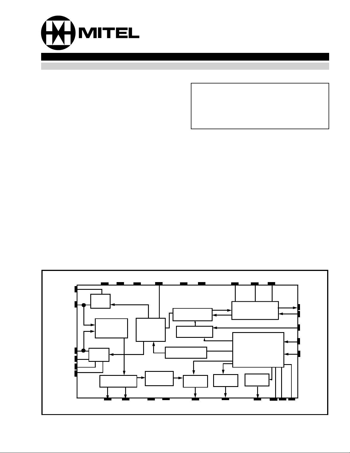
TF
TIP
RING
RF2
RF
VBat
LGND VDD VEE LCA AGND RGND VREF F1i C2i
Tip
Drive
2W/4W
Current
& Voltage
Sensing
Ring
Drive
Line
Supervision
LED SHK VAC VRLY RD1 RD2 RD3 SD5 SD6 SD7
Constant
Current &
Voltage
Control
Auto Ring
Trip Fil te r
Conversion
Gain
Adjust
Tip/Ring
Reversed
Relay
Drive 1
Relay
Driver 2
Filter/Codec
SD2
SD3
SD0
SD1
MT8967
A-Law
8-Bit
Shift
Register
SD4
Relay
Driver 3
Figure 1 - Functional Block Diagram
Do
Di
GS
CS
SDi
2-285

MH89626C Preliminary Information
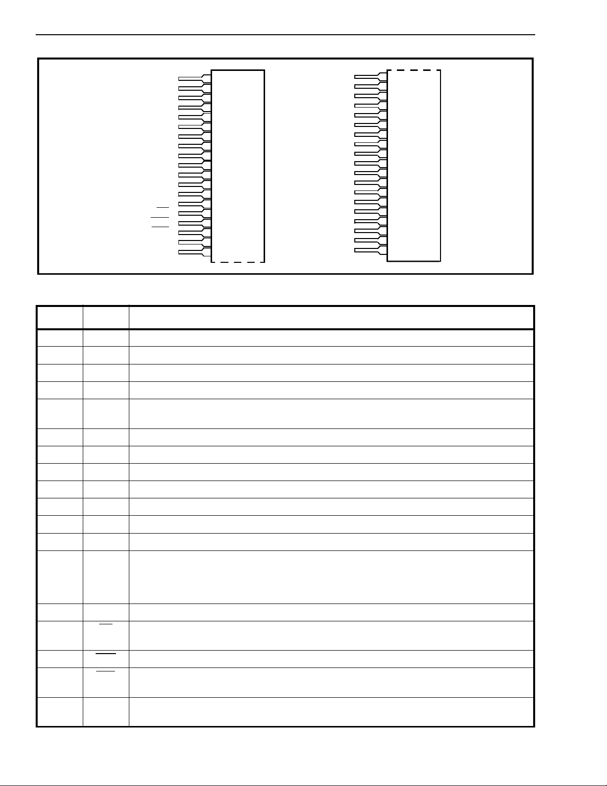
TIP
RING
RF
TF
LPND
VBat
RF1
RF2
VEE
AGND
VDD
IC
VAC
IC
CS
SHK
LED
LCA
SD1
1
2
3
4
5
6
7
8
9
10
11
12
13
14
15
16
17
18
19
VREF
D1
C2i
Do
F1i
IC
IC
IC
GS
IC
SD7
SD6
SD5
IC
VRLY
RGND
RD2
RD3
RD1
Figure 2 - Pin Connections
Pin Description
Pin # Name Description
1TIPTip Lead: Connects to the TIP lead of the telephone line.
2 RING Ring Lead: Connects to the Ring lead of the telephone line.
20
21
22
23
24
25
26
27
28
29
30
31
32
33
34
35
36
37
38
3RFRing Feed.
4TFTip Feed.
5 LGND Loop Ground: Return path for the battery (V
) supply voltage. Connects to System
Bat
Ground.
6V
Battery Supply Voltage: Normally -48V.
Bat
7RF1Ring Feed 1: Ringi ng input .
8RF2Ring Feed 2: Ring ing output.
9V
Negative Su pp ly Voltage. (-5V).
EE
10 AGND An al og Gr ou nd: Analog and Digital Ground. Connects to system ground.
11 V
Positive Su pp ly Voltage. (+5V).
DD
12 IC Internal Connection.
13 VAC Battery AC Component (input). AC noise present in the V
supply isolated from the DC
Bat
components, can be applied to this pin to reduce longitudinal noise on TIP and RING. To
implement this feature, connect a 0.1µF 100V capacitor from V
to VAC, and 1kΩ resistor
Bat
from VAC to AGND. This pin must be tied to AGND when not used.
14 IC Internal Connection.
15 CS
Chip Select (Input): A TTL compatible digit al inp ut to enable the SDi to control all t he
functions of the driver.
16 SHK Switch Hook Detect (Output): A logic low indicates an off-hook condition .
17 LED
LED Drive (Output).: Drives an LED directly through an internal 2.2kΩ resistor. A logic low
indicates an off-hook condition.
18 LCA L oo p Current Adj ust (in pu t): If this pin is left open, the constant current will be set at
23mA. The loop current can be adjusted by connecting a resistor to V
2-286
EE
.

Preliminary Information MH89626C
Pin Description (Continued)
Pin # Name Des crip tio n
19 SDi Serial Data in (input): A TTL compati ble digital input. The 8-bit serial input enables the
driver s. See Table 1 and Figure 3b.
20 V
Voltage Reference (Input) +2.5V for the internal codec.
Ref
21 Di D a ta in (Input) . A TTL compat ibl e digit al input which ac cepts the 8-bit PCM word from the
incoming PCM bu s.
22 C2i Clock input (in pu t). A TTl compatibl e digit al input which ac cepts the 2048 kHz clock.
23 Do Data Out (Output) A three state TTL compatib le digit al out put which drive s the 8-bit PC M
word to the outgoin g PCM bu s.
24 F1i
Synchroni zation input (Inp ut). A TTL compatible, active low digital output input enabling
the PCM input, PCM outp ut and digital control inpu t. It is internally sampled on every
positive edge of the clock, C2i and provides frame and channel synchronization. See fig
3a.
25-27 IC Internal Connection
.
28 GS Gain setting (Input). A logic ‘0’ at this input will set the receiving gain to -7.0dB and a logic
‘1’ will set the receiving gain to -3.5dB. If this pin is left open, the receiving gain can be set
by SDi, bit 2.
29 IC Internal Connection.
30 SD7 S e rial Data (Outpu t). A TTL compatible output comin g from the SDi, bit 7. Bit inverted.
31 SD6 Serial Data (O utput). A TTL compatible output comin g from the SDi, bit 6. Bit inverted.
32 SD5 S e rial Data (Outpu t). A TTL compatible output comin g from the SDi, bit 5. Bit inverted.
33 IC Internal Connection.
34 V
RLY
Relay Positive Supply Voltage. Normally +5V. Connects to the relay coil and the relay
supply voltage.
35 RGND Relay Ground. Return path for relay supply voltage.
36 RD2
Relay Driver 2 (Outpu t). Connects to a user provided external relay coil. A logic ‘0’
from the SDi, bit 1 will activate this driver. This relay driver is typically used for system
in-test.
37 RD3
Relay Driver 3 (Outpu t). Connects to a user provided external relay coil. A logic ‘0’
from the SDi, bit 4 will activate this driver. This relay driver is typically used for system
in-test.
38 RD1
Relay Driver 1 (Outp ut). Connects to a user provided external relay coil. A logic ‘0’ from
the SDi, bit 0 will activate this driver. This relay driver is typically used for ringing.
2-287

MH89626C Preliminary Information
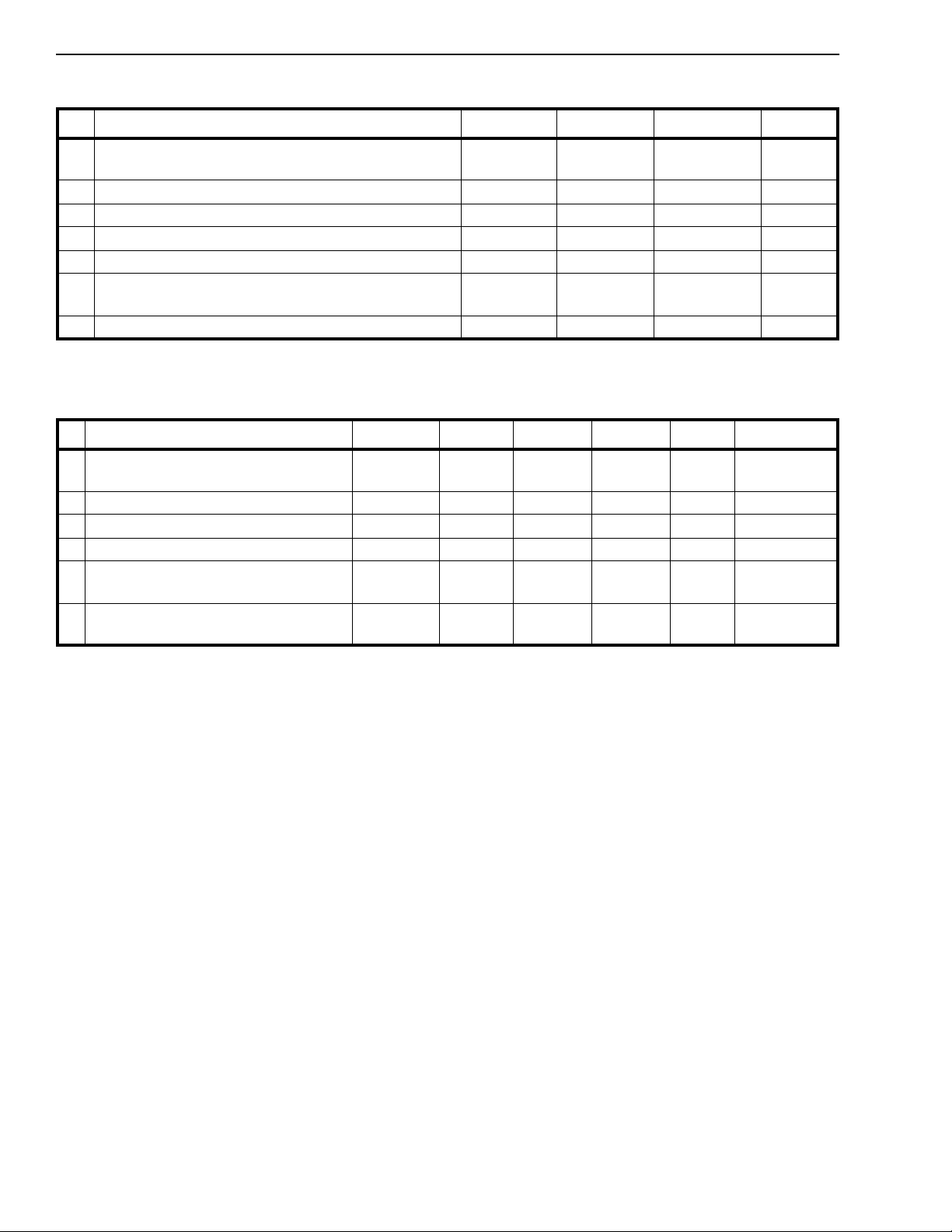
Absolute Maximum Ratings*- All voltages are with respect to AGND unless otherwise specified.
Parameter Symbol Min Max Units
1 DC Supply Voltage V
2 DC Battery Voltages ➀ V
3 DC Ring Relay Voltage V
4 DC Reference Volt age V
V
DD
EE
Bat
RLY
REF
-0.3
0.3
0.3 -65 V
-0.3 7 V
-0.3 V
7
-7
DD
5 AC Ring Generator Voltage 150 V
6 DC Digital Input Voltage GS,SDi,Di,
-0.3 V
DD
C2i,F 1 i
7 Storage Temperature TS -40 +125 °C
* Exceeding these values ma y cause perm anen t dama ge. Functi onal operati on und er these cond ition s is not implied.
Recommended Operating Conditions
Parameter Symbol Min TYP* Max Units Comments
1 DC Supply Voltage V
2 DC Battery Volt age ➀ V
3 DC Ring Relay Voltag e V
4 DC Reference Voltage ② V
5 AC Ring Generator Vol tage
Ringing Generator Frequency
6 Operating Temperature T
V
DD
EE
Bat
RLY
REF
OP
4.75
-4.75
5.0
-5.0
5.25
-5.25
V
V
-39.8 -48 -60 V
5.0 7.0 V
2.488 2.500 2.512 V
22 90
25
130
28
V
RMS
Hz
02570°C
V
V
V
RMS
V
➀ LGND is c o nn ec te d t o AGND
② Temperat ure coefficient of V
should be better than 100ppm/C
REF
2-288
 Loading...