MITEL MH8910-1AC, MH8910-1AP Datasheet
9-3
Features
• Compatible with ISDN U-Interface standard
• Over 40 dB (
@40 kH z) of loop atte nu at io n
• Full dup lex tr ansmi ssi on ov er singl e twis ted
pair
• Adva nced ec ho can cel ling techno logy
• High perf orma nce 2B 1Q line code
• Full act ivatio n/de activ atio n state m ac hine
• QSNR an d line attenu ati on diag nos tics
• Frame and superframe synchronization
• On-chip 15 second timer
• Inser tion loss me asur emen t test signal & quiet
mode
• Mitel ST-BUS compat ible
• Single 5V powe r supp ly
Applications
• ISDN NT1 a nd NT2 DSL interfa ce
• Digita l PABX line cards an d tel ephon e sets
• Digital m ultip lexers an d con cen trators
• Pair gain system
Description
The MT8910-1 Digital Subscriber Line Interface
Circuit (DSLIC)
is designed to provide ISDN basic
rate access (2B+D) at the U-interface. Full duplex
digital trans mission at 160 kbit/s on a single twiste d
pair is achieved using echo cancelling hybrid (ECH)
technology. This, in conjunction with the high
performance 2B1Q line code, allows the DSLIC to
meet the loop length requirements of the digital
subscriber loops at the U-interface over the entire
non-loaded telephone loop plant.
The MT8910-1 is compatible with the complete
range of Mitel Semiconductor ISDN components
through the use of the ST-BUS interface.
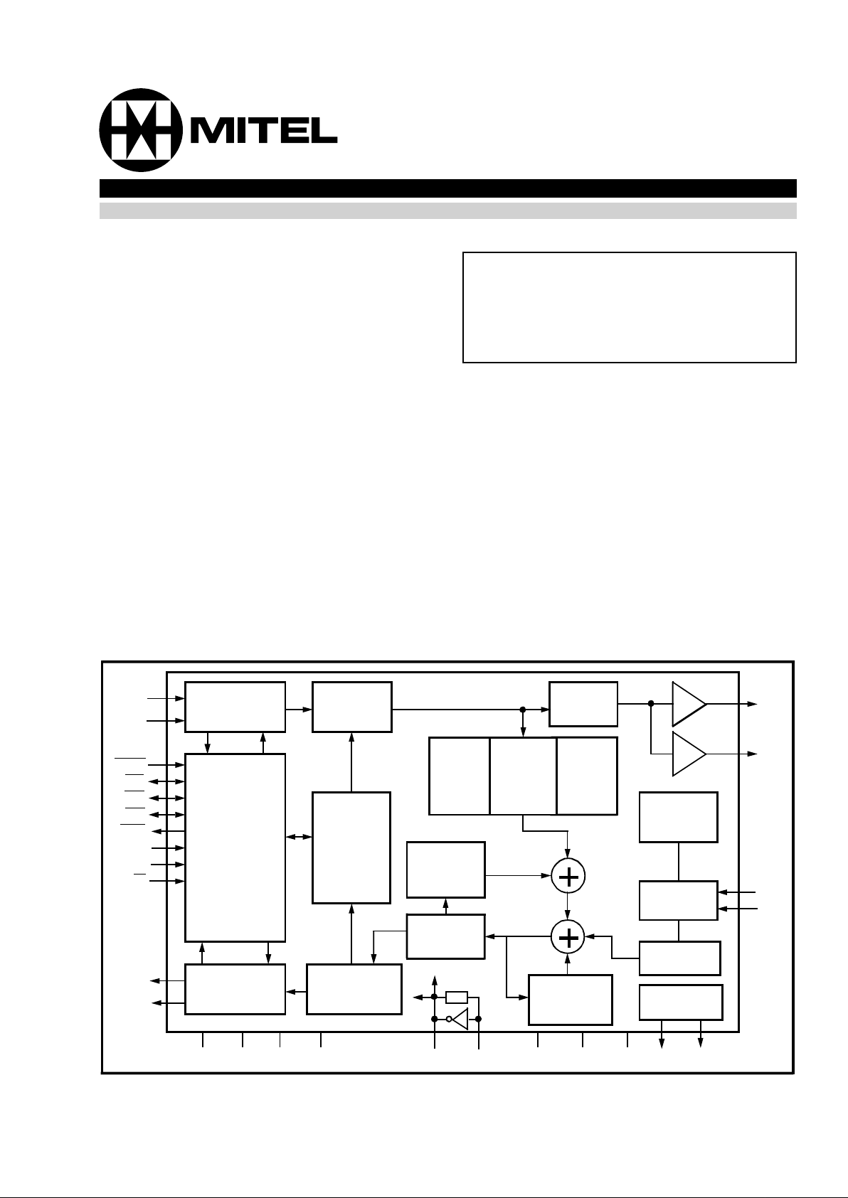
Figure 1 - Functional Block Diagram
DSTi
CDSTi
MRST
F0b
C4b
SFb
F0od
MS0
MS1
NT/LT
CDSTo
DSTo
VSS A VSS VDD A VDD OSC2 OSC1
TSTin TSTout
TSTen
VRef VBias
Lin+
Lin-
Lout-
Lout+
Transmit
Interface
Control
Register
TRANSMIT/
RECEIVE TIMING
& CONTROL
INTERFACE
Status
Register
Receive
Interface
Scrambler
& Encoder
Framing
&
Mainte nance
Descrambler,
Decoder &
Diagnostics
Jitter
Compen-
Linear
Echo
Canceller
Non-
Linear
Compen-
Decision
Feedback
Equalizer
Quantizer
DAC and
Tx Filter
Timing
Adaptation
Circuit
+
-
Tone
Detector
sator
sator
2nd Order
PDM ADC
FIR
Digital Filter
Bias &
Voltage Ref.
Ordering Information
MT8910-1AC 28 Pin Ceramic DIP
MT8910-1AP 44 Pin PLCC
0°C to +70 °C
ISSUE 1 August 1993
MT8910-1
Digital Subscriber Line Interface Circuit
Preliminary Information
CMOS ST-BUS FAMILY
MT8910-1 Preliminary Information
9-4
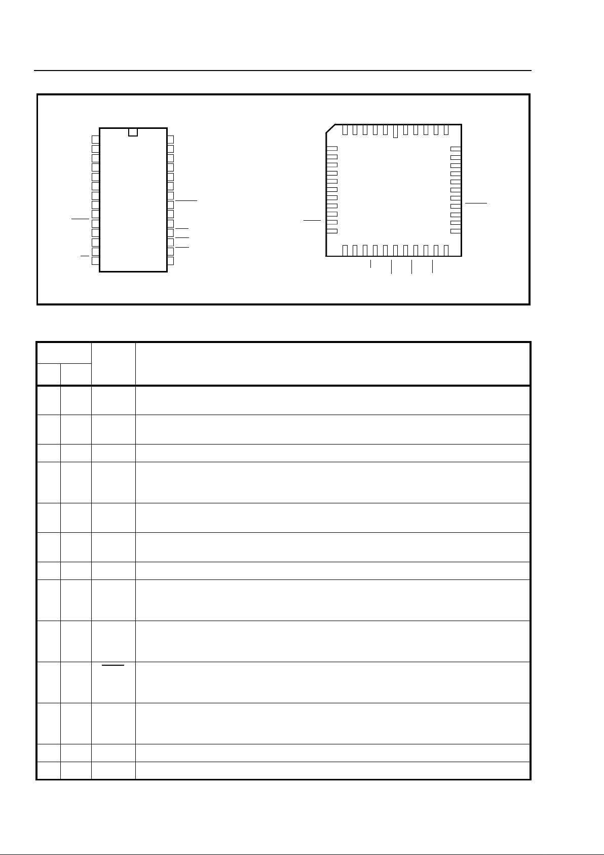
Figure 2 - Pin Connections
Pin Description
Pin #
Name Description
DIP PLCC
11 L
out-
Line Out Minus. One of a pair of differential analog out put s for the 80 kba ud/ s 2B1Q
signal, biased at V
Bias
.
23 L
out+
Line Out Plus. One of a pair of differential analog outputs for the 80 kbaud/s 2B1Q signal,
biased at V
Bias
.
35AV
SS
Analog Ground. Tie to VSS.
46TSTinI/O Structure Test Input. When TSTen is high, TSTin is used as a source to all output
drivers. Refer to “I/O Structure Test" in functional description for more details. Tie to V
SS
for normal operation.
5 8 CDSTi Control/Data ST-BUS Input. A 2048 kbit/s serial PCM/data input for the D- and
C-channels in Dual mode. Unused in Single mode and should be connected to V
SS
.
612DSTiData ST-BUS Input. A 2048 kbit/s serial PCM/dat a input for the D-, C-, B1- and B2-
channels in Single mode. In Dual mode, only the B- channels are input .
713 V
SS
Ground .
814DSToData ST-BUS Output. A 2048 kbit/s serial PCM/data output for th e D-, C-, B1- and B2-
channels in Single mode. In Dual mode, only the B- channels are outp ut. This output is
placed in high impedance during the unused channel times.
9 15 CDSTo Control/Data ST-BUS Output. A 2048 kbit/s serial PCM/data output for the D- and
C- channels in Dual mode. It is placed in high impedance in Single mode, and during the
unused channel times in Dual m o de.
10 16 F0od
Delayed Frame Pulse Ou tput. A 244 ns wide negative going pulse indicat ing the end of
the active ST-BUS channel times of the device to allow for daisy-chaining of other ST-BUS
devices. Active after channel 0 in Dual Port mode and Channel 3 in Single Port Mode.
11 18 TSTout I/O Structure Test Output. When TSTen is high, the TSTout provides the output of an
XOR chain which is sourced from all digital inputs. Refer to “I/O Structure Test" in
functional description for more deta ils. Leave unconnected for normal operation.
12 19 MS0 Mode Select 0. CMOS input. Refer to Table 1.
13 20 MS1 Mode Select 1. CMOS input. Refer to Table 1.
44 PIN PLCC
1
2
3
4
5
6
7
8
9
10
11
12
13
14
15
16
17
18
19
20
28
27
26
25
24
23
22
21
Lout-
Lout+
AVSS
TSTin
CDSTi
DSTi
VSS
DSTo
CDSTo
F0od
TSTout
MS0
MS1
NT/LT
Lin+
LinVRef
VBias
AVDD
IC
VDD
MRST
OSC1
OSC2
F0b
C4b
SFb
TSTen
28 PIN CERDIP
TSTin
AVSS
Lout+NCNC
Lin+
Lin-
VRef
VBias
NC
TSTout
MS0
MS1
NT/LT
TSTen
NC
C4b
NC
F0b
NC
SFb
Lout-
1
65432 44434241
40
7
8
9
10
11
12
13
14
15
16
39
38
37
36
35
34
33
32
31
30
231819202122 2425262728
17
29
NC
AVDD
NC
NC
NC
IC
VDD
MRST
OSC1
OSC2
NC
NC
CDSTi
NC
NC
NC
DSTi
VSS
DSTo
CDSTo
F0od
NC
Preliminary Information MT8910-1
9-5
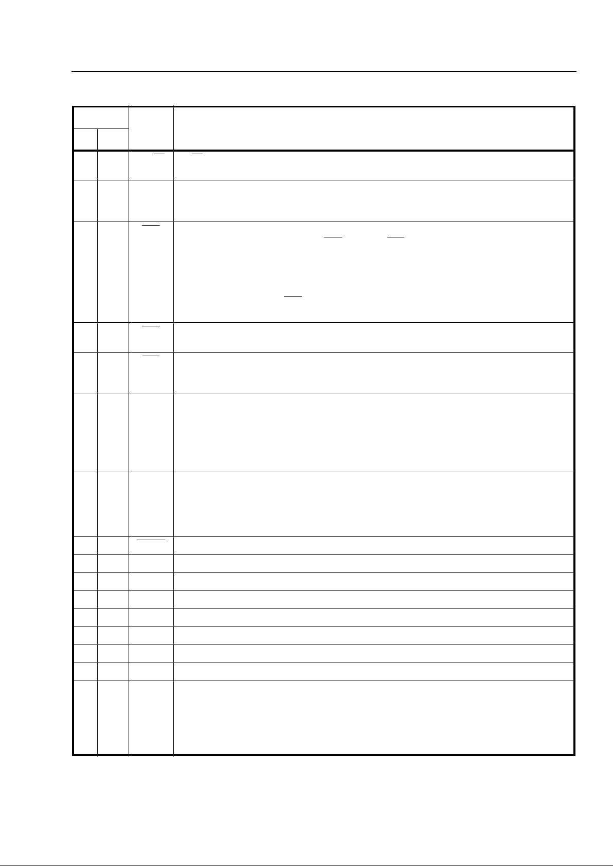
14 21 NT/LT NT/LT Mode Select. CMOS Input. When high, the DSLIC is setup in NT mode. When
low, LT mode is selected.
15 22 TSTen I/O Structure Test Enable Input. This active high input enables the bui lt-in test of all
digital input and output structures. Refer to “I/O Structure T est" in functional description for
more details. Tie to V
SS
for normal operation.
16 23 SFb
Superframe Pulse. In LT mode, an input pulse once every superframe (12 ms) which,
when low during a falling edge of C4 b
within an F0b low pulse, sets the transmit
superframe boundary.
In NT mode, a 244 ns wide output pulse once every 12 ms indicating the boundary of the
transmit superframe. In NT mode, the superframe timing is generated from the line signal
time base and, as such, SFb will only be valid once the transceiver has achieved full
activation.
17 25 C4b
4096 kHz Data Clock. In LT mode, a 4096 kHz ST-BUS clock input. In NT mode, a 4096
kHz ST-BUS clock output frequency locked to the line signal.
18 27 F0b
Frame Pul se. In LT mode, an 8 kHz input pulse indicating the start of the active ST-BUS
channel times. In NT mode, an 8 kHz output pulse extracted from the line signal indicating
the start of the active ST-BUS channel times.
19 30 OSC2 Oscillator Outpu t. When the MT8910-1 operate s with an External Clock (typicall y LT
mode) connect OSC2 to the output of an external inverter providing a 10.24 MHz ±5ppm
clock (see “10.24 MHz Clock Interface" section).
When operating wit h a crystal (typically NT mode) connect one lead of the fundament al
mode parallel resonator crystal (10.24 MH z ±50ppm in case of NT mode).
20 31 OSC1 Oscillator Inpu t. When the DSLIC operat es with an External Clock (typical ly LT mode)
connect OSC1 to the input of an external inverter (see Fig.11).
When operating wit h a crystal (typically NT mode) connect the other lead of the
fundamental mode parall el resonato r crystal (10.24 MHz ±50ppm in case of NT mode).
21 32 MRST
Master Reset. Active low CMOS input perform s a maste r reset of the DSLIC.
22 33 V
DD
Power Supp ly Input.
23 34 IC Internal Connection. Leave unconnected.
24 38 AV
DD
Analog P ow er Su pp ly. Connect to VDD.
25 41 V
Bias
Bias Vol tage. Decouple to AVSS through a 1.0 µF ceramic capacitor.
26 42 V
Ref
Reference Voltage. Decouple to AVSS through a 1.0 µF ceramic capacitor.
27 43 L
in-
Line Signal Input Minus. Internally biased at V
Bias.
28 44 L
in+
Line Signal Input Plus. Internally biased at V
Bias.
2,4,7,
9 -11,
17,24
26,28
29,35
36,37
39,40
NC No Connection. Leave circuit open.
Pin Description (continued)
Pin #
Name Description
DIP PLCC

MT8910-1 Preliminary Information
9-6
Functional Description
The MT8910-1 Digital Subscriber Line Interface
Circuit (DSLIC) is a high performance, full duplex
transceiver which provides a complete interface to
the U-reference point as specified in ANSI T1.601-
1988. Operating in either master Line Terminator
(LT) mode or slave Network Terminator (NT) mode,
the DSLIC can be configured to operate at either end
of the Digital Subscriber Line (DSL). The DSLIC
supports full duplex transmission of a 2B + Dchannel format at 160 kbit/s over a single twisted
pair with about 40 dB of loop attenuation at 40 kHz.
To achieve this transmission performance, the
DSLIC uses a 2B1Q line code which is a four level
pulse amplitude modulated (PAM) signal with no
redundancy. This line code was approved by the
American National Standards Institute technical
committee T1E1. Using this line code, two binary
bits are converted into one four level quaternary
symbol. This results in an effective baud rate
reduction from 160 to 80 kbaud/s allowing the
transmission to benefit from reduced line attenuation
and improved immunity to near end crosstalk
(NEXT).
To complement the performance of the 2B1Q line
code, the DSLIC uses an advanced echo cancelling
hybrid (ECH) technique, by means of a transversal
filter, that provides greater than 60 dB of echo
cancellation. This cancellation, along with all
equalization, is performed in the digital domain using
dedicated DSP hardware. Since a digital transversal
echo canceller gives a linear representation of the
echo, the MT8910-1 also has a non-linear echo
canceller which works in parallel with the transversal
filter t o compensate for non-linearities in the transmit
path and the passive line termination. In addition, a
jitter compensator is used to correct errors in the
echo estimates which are sourced from corrections
in the received timebase. The jitter compensator will
interact directly with the echo taps in the transversal
filter.
A block diagram of the DSLIC is shown in Figure 1.
The DSLIC has two ports consisting of a serial
system interface (Mitel's standard ST-BUS), and a
line port which interfaces directly to the single
twisted pair via a passive termination hybrid and a
line pulse transformer.
The two B-channels and the D-channel to be
transmitted on the line are input to the DSLIC (on the
ST-BUS) into the transmit interface block. The sync
word and maintenance bits are added to the data
which is then formatted, scrambled and digitally
encoded into 2B1Q symbols. This digital
representation is passed through a finite impulse
response filter which converts the digital
representation into an analog waveform. The
transmitted pulse is then passed through a
smoothing filter whose output is passed to a
differential line driver which is driving t he line through
a passive hybrid network and line pulse transformer.
On the receive side, the pre-cancelled signal drives
a balanced receiver which feeds the input to an oversampled second-order delta sigma A/D converter.
The digital representation of the received signal
yields a Pulse Density Modulated (PDM) stream
which is digitally filtered and decimated to the 80 kHz
baseband. Intersymbol interference (ISI) introduced
by the loop is cancelled by a decision feedback
equalizer. This is achieved by taking a convolut ion
of the received pulse with the estimated impulse
response of the loop. The cancellation of ISI is
performed in parallel with the echo cancellation.
Estimated received echo is obtained by taking the
convolution of the transmit signal with the estimated
impulse response of the loop. Feedback from the
jitter compensator and the non-linear corrector
interact with the coefficients of the echo canceller to
reduce the error introduced by jitter and nonlinearities in the analog circuitry. The output of all
these blocks is summed together and the result is
the received data which is passed through a decoder
and descrambler before being sent out in TDM
bursts on the ST-BUS.
Line Port
The DSLIC interfaces to the U-reference point as
defined in the ISDN Basic Access Reference model.
As such, the transceiver transfers full duplex, time
division multiplexed data at 160 kbit/s. This includes
two 64 kbit/s PCM voice or data channels (Bchannels), a 16 kbit/s signalling channel (D-channel)
and 16 kbit/s for synchronization and overhead.
The two 64 kbit/s channels are defined as the B1and B2-channels and they carry subscriber
information such as digitally encoded voice, circuit
switched data or packet switched data. The DSLIC
will transfer both B-channels transparently from the
ST-B US port to the line port and vice versa once the
device has acquired superframe synchronization.
The 16 kbit/s D-channel is primarily intended to carry
signalling information for circuit switching the Bchannels through the ISDN network. The D-channel
can optionally carry packetized information and
telemetry services. The D-channel is transmitted
transparently through the DSLIC from the ST-BUS
port to the line port and vice versa once the device
has acquired superframe synchronization. It is to be

Preliminary Information MT8910-1
9-7
noted that the system interface has dedicated a full
64 kbit/s for the D-channel of which only the two first
bits (D0 and D1) are actually carrying information.
The other bits of the ST-BUS D-channel ar e reserved
for future use.
A third type of channel, the C-channel, is a nonbearer channel which provides a means for the
system to control and monitor the functionality of the
DSLIC. This control/status channel is accessed by
the system through the ST-BUS. The C-channel
provides access to three control registers and four
status registers which provide complete control or
status of all built-in features. Access to the control
register is provided by two bits in the Control
Register itself (CRS0 and CRS1). Selection of the
desired status register is performed using two bits in
Control Register 1 (SRS0 and SRS1). The Cchannel also carries a control and status register for
the 4 kbit/s M-channel which can be used as an
additional maintenance channel. A detailed
description of these registers is discussed in the STBUS port interface section.
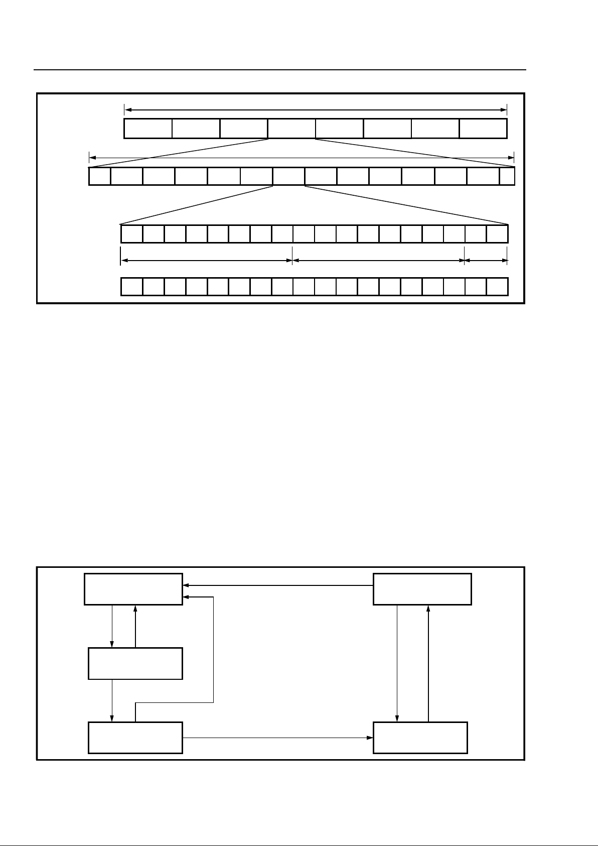
Line Code
The DSLIC transceiver uses the 2B1Q line code
which is a four level Pulse Amplitude Modulated
(PAM) code with no redundancy. The generation of
the 2B1Q signal is achieved by grouping two
consecutive bits into a bit field of which the first bit
represents the sign bit and the second represents
the magnitude. This yields four possible output
codes as shown in Figure 3 (note that +3, +1, -1 and
-3 are only symbols and they do not reflect the
voltage on the line).
The bit fields are grouped relative to the borders of
the defined channels where the first bit field consists
of bit 1 and bit 2 of the B1-channel, the second bit
field consists of bit 3 and bit 4 of the B1-channel
and so on.
Before conv erting the bit fields into outp ut symbols,
all bits except the framing pattern are scrambled with
polynom i als:
1
⊕ x
-5
⊕ x
-23
for LT
1
⊕ x
-18
⊕ x
-23
for NT
(where
⊕ is modulo two summation)
Framing
The frame structure in the DSLIC is 1.5 ms long and
consists of twelve 2B+D-channels delimited by the
framing pattern at the start of the frame and the
maintenance channel at the end. Framing for both
the LT and the NT is performed using a 9 symbol
synchronization word. This sync word (SW) has the
following structure:
Sync Word: + 3, + 3 , -3, -3, -3, +3 , - 3, + 3 , + 3
Eight DSLIC frames are grouped into a superframe
delimited by inverting the sync word (ISW):-3,-3, +3,
+3, +3, - 3 , +3 , -3, -3. This seco nd l ev e l o f framing is
used to assign the M-channel bits as defined in the
ANSI T1.601-1988. The framing structure is shown
in Figure 4.
Transmission between the LT and NT is fully
synchronous. As such, the frame/superframe
boundaries between the NT receive frame and the
NT transmit frame have a fixed phase relationship.
The transmitted frame/superframe from the NT is
delayed by 60 ± 2 quaternary symbols (quats) with
respect to its received frame/superframe. Since the
NT extracts all its timing fro m the line, the D SL IC w i ll
maintain the required phase relationship between
the frames and superframes and will insert the SW
and ISW during the proper time interval.
Figure 3 - Example of 2B1Q Quaternary Symbols
+3
+1
-1
-3
time
QUATS -1 +3 +1 -3 -3 +1 +3 -3 -1 -1 +1 -1 -3 +3 +3 -1 +1
BITS 0 1 1 0 1 1 0 0 0 0 1 1 1 0 0 0 0 1 0 1 1 1 0 1 0 0 1 0 1 0 0 1 1 1
MT8910-1 Preliminary Information
9-8
Figure 4 - F rame S truc ture
12 ms
1.5 ms
50 µs
50 µs
12.5 µs
Superframe
Frame
Information
Channels
Corresponding
ST-BUS
Frame 1 Frame 2 Frame 3 Frame 4 Frame 5 Frame 6 Frame 7 Frame 8
SW 2B + D 2B + D 2B + D 2B + D 2B + D 2B + D 2B + D 2B + D 2B + D 2B + D 2B + D 2B + D M
B11 B12 B13 B14 B15 B16 B17 B18 B21 B22 B23 B24 B25 B26 B27 B28 D1 D2
B7 B6 B5 B4 B3 B2 B1 B0 B7 B6 B5 B4 B3 B2 B1 B0 D0 D1
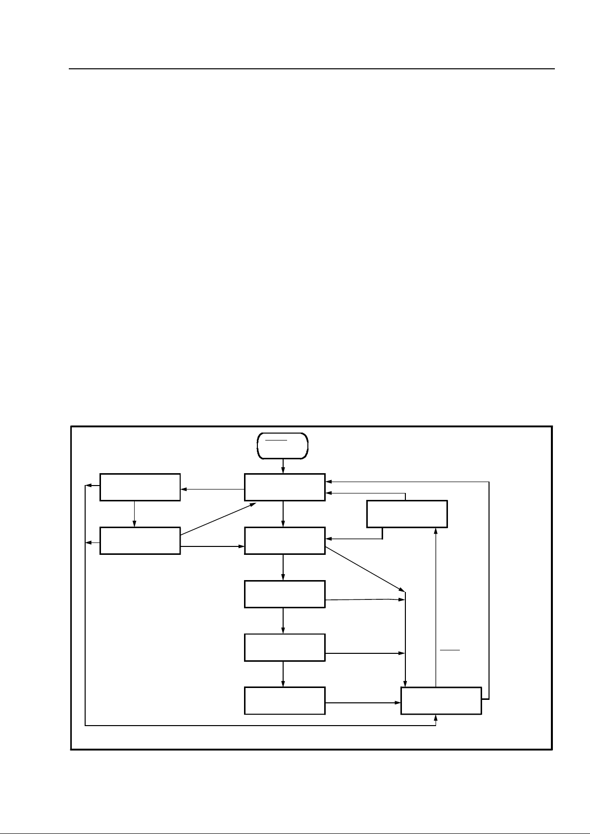
Basic Frame Synchronization (BFS) is achieved
using the algorithm shown in Figure 5. The DSLIC
searches for the sync word or the inverted sync word
within the received data stream. After detecting
three consecutive synchronization patterns spaced
exactly 120 quats apart, the DSLIC declares terminal
synchronization by setting the bits of the Internal
State Indicator to 111 in Status Register 1. A loss of
synchronization is declared by the DSLIC when at
least one of the nine quats at the beginning of each
Basic Frame differs by more than one quantization
level for two consecutive frames.
A search for superframe synchronization will begin
only after Basic Frame sync has been found. The
DSLIC will declare superframe sync (SFS) on the
first occurrence of the properly spaced Inverted Sync
Word (ISW) once Basic Frame sync has been
acquired. The synchronized state is identified by the
status of internal state bits IS2, IS1 and IS0 found in
Status Register 1.
The DSLIC will lose superframe sync under three
conditions;
1) if the DSLIC loses basic frame sync,
2) if the ISW does not occur exactly eight basic
frames apart,
3) if the ISW is received w hen it is not expected.
Activation/ De activ atio n
The DSLIC has a complete activation/deactivation
state machine which allows the user to activate or
deactivate the link as per the requirements in the
Figure 5 - Frame Synchronization State Diagram
STATE : LOST
BFS : 0
One
Valid
SW
Error in
SW
STATE : SENSING1
BFS : 0
One
Valid
SW
STATE : SENSING2
BFS : 0
One Valid SW
> One-Level Error in SW
STATE : LOSING
BFS : 1
> One-Level
Error in SW
Valid
SW
STATE : SYNC
BFS : 1
Error in
SW
Preliminary Information MT8910-1
9-9
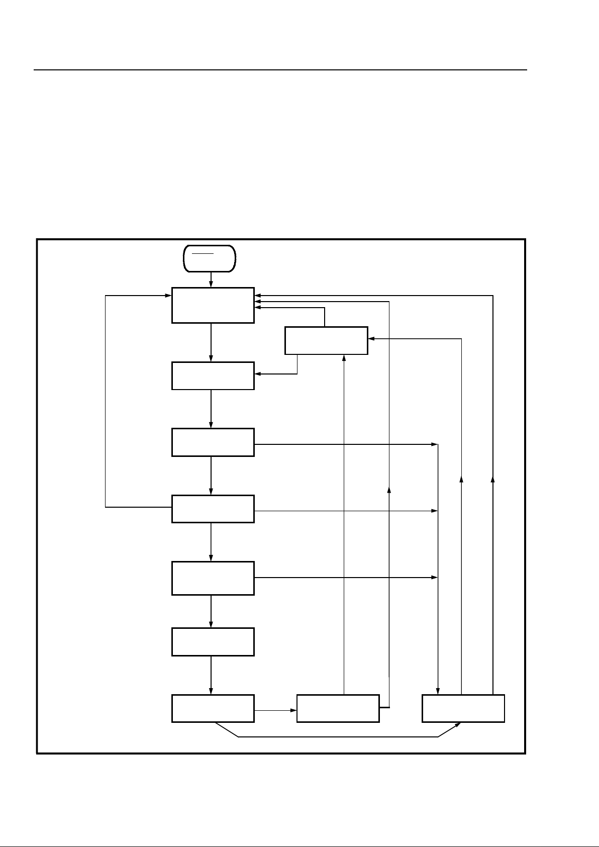
T1.601-1988 standards. The activation sequence for
the DSLIC is mode dependent and is outlined in
Figures 6a) and b).
In the LT mode, the request for activation can be
initiated in two w ay s. Se tting the st art/s top bit in the
Control Register 1 will result in the generation of a
repeated pattern of four +3 symbols followed by four
-3 symbols producing a 10 kHz activation tone (TL)
for 3 milliseconds. The DSLIC can also be activated
by receiving a 10 kHz activation tone from the NT
(TN). Once the NT has generated a tone,
progression through the state machine follows the
algorithm as s hown in Figure 6a.
In the NT mode, the request for activation can be
initiated in two w ay s. Se tting the st art/s top bit in the
Control Register 1 will result in the generation of a
repeated pattern of four +3 symbols followed by four
-3 symbols resulting in the transmission of the NT
activation tone (TN). The DSLIC can also be
activated by receiving TL from the LT to which the
NT will respond with its own activation tone (TN).
Progression through the state machine will follow the
algorithm as s hown in Figure 6b.
During the activation sequence, there is an extensive
exchange of signals between the LT and the NT.
This handshaking of information is required to allow
individual transceivers to train both their echo
cancellers and decision feedback equalizers. All
possible signals are described below.
• TN: A 10 kHz activatio n t on e s ourced by t he
NT which is ge nerat ed by sen ding a
continuo us pa ttern o f fou r +3 s ymbol s
followed by four -3 symbols.
• SN0: SN0 is a no signal condition which is
used to ind ica te to the LT that the N T
has finish ed trai ning its ech o can celle r.
• SN1: An NT generated signal consisting of a
framed (b ut not su per framed ),
scrambled 2B1Q signal which carries all
1s in the B-, D- and M-channels. This
signal is us ed t o train t he NT’s ech o
canceller.
• SN2: An NT generated signal consisting of a
framed (b ut not su per framed ),
scrambled 2B1Q signal which carries all
1s in the B-, D- and M-channels. This
signal is us ed t o train t he LT’s DFE.
• SN3: An NT generated signal consisting of a
fully framed and superframed scrambled
2B1Q si gn al w hi ch c ar ri es i nf orm at io n in
all the B-, D- and M-channels.
Figure 6a - Acti vatio n/Deac tiva tion State Diagra m - LT Mode
Alerting
Tx-TL (3ms)
Awaiting Reply
Tx-SL0
MRST
Pin
Full Reset
Tx-SL0
Awake
Tx-SL0
EC Training
Tx-SL1
Framing
Tx-SL2
Active
Tx-SL3
RCV Reset
Tx-SL0
Pending Deact.
Tx-SL0
LAR
ST.T0
Expiry of T2
RCV TN
ST.T0
STP.T2
Expiry
of T0
Expiry of T0
Expiry of T0
BFS Lost > 480ms
1
or LDR
ST.T3
ST.T3
(Loss of
signal and
LDR),
ST.T2
STP.T3
(Loss of signal
and LDR) or
Expiry of T3
RCV TN
ST. T0
End SN1
EC
Converged
SFS
STP.T0
Expiry of
T1
RCV TN
STP.T1
Expiry of T0
ST.T3
ST.Tx = Start Timer x
STP.Tx = Stop Timer x
LAR = Local Activation Request
LDR = Local Deactivation Request
SFS = Superframe Synchronization Acquired
T0 = 15 sec timer
T1 = 480 ms timer
T2 = 40 ms timer
T3 = 520 ms timer
Note
1
: Loss of received signal will result in loss of sync.
ST.T1
MT8910-1 Preliminary Information
9-10
• TL: A 10 kH z act i v atio n t one sourced by the
LT which i s genera ted b y send ing a
continuo us pa ttern o f four +3 sym bo ls
followed by four -3 symbols.
• SL0: SL0 is a no si gnal cond ition ge ne rated
from the LT.
• SL1: An LT generated signal consisting of a
framed (b ut not su pe rframed ),
scrambled 2B1Q signal which carries all
1s in the B-, D- and M-channels. This
signal is us ed t o train t he LT’s echo
canceller.
• SL2: An LT generated signa l co nsis ting of a
fully framed and sup erfram ed
scrambled 2B1Q signal which carries all
0s in the B- a nd D-c hanne ls w ith
information i n the M-chan nel. Th is
signal is used to train the NT’s DFE.
• SL3: An LT generated signa l co nsis ting of a
fully framed and superframed scrambled
2B1Q signal which carries information in
all the B-, D - and M- chan nels.
Figure 6b - Activ atio n/Deac tivation State Diagra m - NT Mod e
MRST Pin
Full Reset
(Power down
Tx-SNO
RCV TL or
LAR
ST.T0
Expiry of T2
RCV Reset
Tx-SN0
Alerting
Tx-TN (9 ms)
EC Training
Tx-SN1
Expiry of T0
Expiry of T1
Quiet
Tx-SN0
Expiry of T0
Signal
Detected
STP.T1
Expiry of T0
Train
DFE/Timing
Tx-SN0
SL2
Detected
Framing
Tx-SN2
SFS
Active
Tx-SN3
LDR
ST.T3
Pending Dea ct.
Tx-SN3
Loss of
far-end
signal
STP.T3
ST.T2
ST.T3
ST.T3
Expiry
of T3
Loss of signal
STP.T3
ST.T2
Tear Down
Tx-SN0
Loss of BFS > 480ms
1
ST.T3
ST.Tx = Start Timer x
STP.Tx = Stop Timer x
LAR = Local Activation Request
LDR = Local Deactivation Request
SFS = Superframe Synchronization Acquired
T0 = 15 sec timer
T1 = 480 ms timer
T2 = 40 ms timer
T3 = 520 ms timer
Note
1
: Loss of received signal will
result in a loss of sync.
EC
Converged
ST.T1
RCV TL
ST.T0
STP.T2
 Loading...