MITEL MH88622-3, MH88622-5, MH88622-1, MH88622-2 Datasheet

MH88622
DUAL OPS SLIC
Preliminary Info rm atio n
Features
•Dual SLIC
• Ringing generation
• On-hook t rans missi on
• Transformerless 2-4 wire conversion
• Constan t c u rrent feed
• Battery Feed to the line
• Tip Ring reversal cap ability
• Over current pro tecti on
• Off-Hook detecti on
• Logic interface for SHK
, RC, LR, ESE, LCS
• Metering injection
•Wide V
operatin g range
Bat
• Minim um in sta lla tio n s pa ce
• ESE ramped output
Applications
•Pair Gain
•CT2
• Cordless local loops
ISSUE 3 April 1995
Ordering Information
MH88622 -1, -2, -3,-5 40 Pin SIL Package
0°C to 70°C
Description
The Mitel MH88622 is a Dual Subscriber Interface
Circuit which provides a complete interface between
the telephone lines a dual codec, requiring a dual rail
supply, battery and dc supply for ringing generation.
The functions provided by the MH88622 includes 2-4
Wire conversion, constant current line feed,
signalling and control. The SLIC manufactured using
thick film hybrid technology which offers high voltage
capability, reliability and high density resulting in a
significant area saving on the printed circuit board. A
complete C.O. type solution can be implemented
with minimal external components. Different variants
are provided to meet different country line
impedance, they are:
-1 220Ω + (820 Ω // 115nF)
-2 600Ω
-3 370Ω + (620 Ω // 310nF)
-5 200Ω + (680 Ω // 100nF)
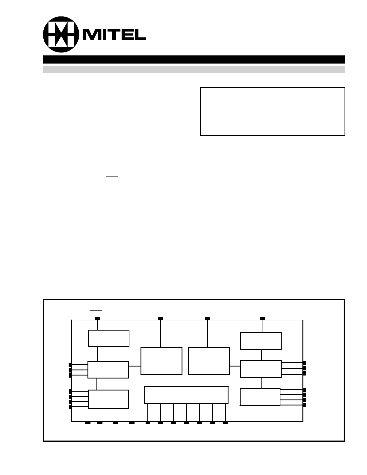
LR1
TIP1
RING1
VX1
VR1
ESI1
ESE1
SHK1
Loop
Supervision
Line Drivers/
Feed
2-4 Wire
Conversion
VDD VEE AGND VBat DCRI RC1 RF1 RF2 RGV RG1 RC2
LCS1
Over Current
Protection &
Constant
Current Feed
Ring Generator
LCS2
Over Current
Protection &
Constant
Current Feed
Figure 1 - Functional Block Diagram
SHK2
Loop
Supervision
Line Drivers/
Feed
2-4 Wire
Conversion
LR2
TIP2
RING2
VX2
VR2
ESI2
ESE2
2-173

MH88622 Preliminary Information
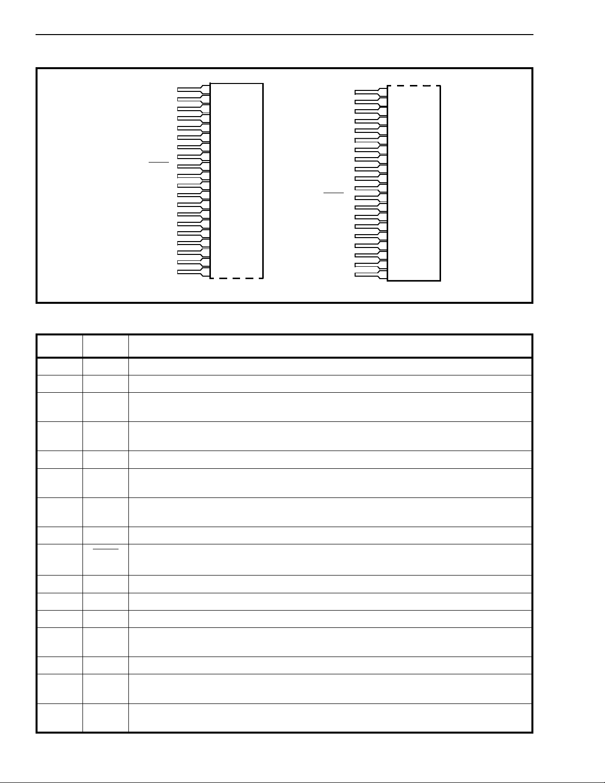
TIP1
RING1
VBAT
DCRI
GND
ESI1
ESE1
VR1
SHK1
LCS1
VX1
VEE
GND
VDD
LR1
RC1
NC
NC
RF1
RF2
1
2
3
4
5
6
7
8
9
10
11
12
13
14
15
16
17
18
19
20
RGV
RG1
NC
NC
RC2
LR2
VDD
GND
VEE
VX2
LCS2
SHK2
VR2
ESE2
ESI2
GND
DCRI
VBat
RING2
TIP2
Figure 2 - Pin Connections
Pin Description
Pin # Name Description
1TIP1Tip Lead. Connects to the “TIP” lead of subscriber line 1.
21
22
23
24
25
26
27
28
29
30
31
32
33
34
35
36
37
38
39
40
2RING1Ring Lead . Connects to the “RING” lead of subscriber line 1.
3V
BAT
Battery V oltage. Typically -48V dc is applied to this pin. This should be connected to pin 38
of the hybrid on the PCB.
4 DCRI DC Ringing Voltage Input. A continuous 120V dc is applied to this input to achieve
90Vrms ringing. This should be connected to pin 37 of the hybrid.
5GNDGround . This pin should be tied to pins 13, 28 & 36 on the PCB.
6ESI1External Signal Input (Input). A continuous signal should be applied to this pin which will
be switched to “Tip” and “Ring” of subscriber 1.
7ESE1External Signal Enable (Input). The external signal to the subscriber 1 is controlled by a
logic level applied to this pin.
8VR1Receive (Input). 4-Wire GND ref erenced audio input for sub scrib er 1.
9SHK1
Off Hook Indication (Outpu t). A logic low out put indicates when subscriber 1 equipmen t
has gone off hook.
10 LCS1 Loop Curr ent Set 1. Logic 1 gives I
= 40mA, Logic 0 gives I
Loop
Loop
= 25mA
11 VX1 Transmit (Output). 4-Wire, GND referenced audio output for subscriber 1.
12 VEE Negative Supply Voltage. -5Vdc. Connects to pin 29 of the hybrid on the PCB.
13 GND Ground . Return path for VDD, VEE, VBat & DCRI. This pin should be connected to pins 5,
28 & 36 of the hybrid on the PCB.
14 VDD Positive Supp ly Voltage. +5Vdc. Connect to pin 27 of the hybrid on the PCB.
15 LR1 Line Reversal. A logic 1 applied to LR1 will reverse the “Tip” and “Ring” to subscriber 1.
This pin has an internal pull down.
16 RC1 Ringi ng Con trol (Inpu t). A logic level applied to this pin enables ringing to be applied
across Tip and Ring of subscriber 1.
2-174

Preliminary Information MH88622
Pin Description (Continued)
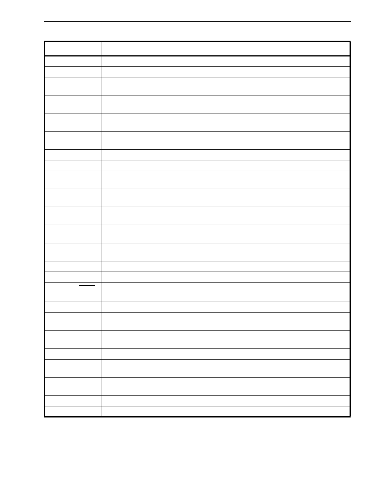
Pin # Name Description
17 NC No Connection. This pin should not be connected.
18 NC No Connection. This pin should not be connected.
19 RF1 Ring ing Fr equ ency Node 1 (Input). A capacitor is connected betwe en RF1 & RF2 and
determine s the frequency of the ringing generator.
20 RF2 Ring ing Fr equ ency Node 2 (Input). Two capacitors are connected between RF1& RF2
and from RF2 to AGND. This determines the frequency of the ringing generator.
21 RGV Ri ng ing Ga in Voltage. Connects to RG1 through a resistor to reduce the output ringing
voltage. When left open circuit output ringing volt age is 90Vrms.
22 RG1 Ringing Gain Node 1. Connects to RGV thro ugh a resistor to reduce the output ringing
voltage. When left open circuit output ringing volt age is 90Vrms.
23 NC No Connection. This pin should not be connected.
24 NC No Connection. This pin should not be connected.
25 RC2 Ringi ng Con trol (Inpu t). A logic level applied to this pin enables ringing to be applied
across Tip and Ring of subscriber 2.
26 LR2 Line Reversal. A logic 1 applied to LR2 will reverse the “Tip” and “Ring” to subscriber 2.
This pin has an internal pull do wn.
27 VDD Positive Supp ly Voltage. +5Vdc. This pin should be connected to pin 14 of the hybrid on
the PCB.
28 GND Ground . Return path for VDD, VEE, VBat & DCRI. This pin should be connected to pins 5,
13 & 36 of the hybrid on the pcb.
29 VEE Negative Supply Voltage
the PCB.
30 VX2 Transmit (Output). 4-Wire GND referenced audio inpu t for subscriber 2.
31 LCS2 Loop Curr ent Set 2. Logic 1 gives ILoop = 40m A, Logic 0 gives ILoop = 25mA.
32 SHK2
33 VR2 Receive (Input). 4-Wire GND referenced audio input for subscriber 2.
34 ESE2 External Signal Enable (Input). The external signal to subscriber 2 is controlled by a logic
35 ESI2 Exter nal Signal Input. A continuous signal should be applied to this pin which will be
36 GND Ground . This pin should be tied to pins 5, 13 & 28 on the PCB.
37 DCRI DC Ringin g Voltage Input. A continuous 120Vdc is applied to this input to achieve 90
Off Hook Indication (Outpu t). A logic high output indicat es wh en sub scriber 2 equi pme nt
has gone off hook.
level applied to this pin.
switched to “Tip” and “Ring” of subscriber 2.
Vrms ringing. This should be connected to pin 4 of the hybrid on the PCB.
. -5Vdc. This pin should be connected to pin 12 of the hybrid on
38 VBAT Battery Voltage. Typically -48V dc is applied to this pin. This should be connected to pin 3
of the hybrid on the PCB.
39 RING2 Ring Lead. Connects to the “Ring” lead of subscriber line 2.
40 TIP2 Tip Lead. Connects to the “Tip” lead of subscriber line 2.
2-175
 Loading...