MITEL MH88620IN Datasheet

MH88620IN
C.O. SLIC
Preliminary Information
Features
• 600 ohm inp ut imp eda nce
• Externally s electa ble net work ba lanc es
• Transformerless 2-4 wire conversion
• Programmab le c onsta nt resis tan ce feed
• Off-hook and dial pulse detection
• High immunity to externally induced longitudinal
currents
• Auto ring trip
• On-hook tran smissi on (A NI) cap ability
• Minimum p rotecti on circ uitry requi red
• Compatible with requ irem ents of CDOT D OC/
FCC, CSA/UL,CCITT
• Excellent power dissipation (SIL vertical
mountin g)
Applications
• On/Off-Premise PBX Line Cards
• Central Offic e Line C ard s
ISSUE 3 April 1995
Ordering Information
MH88620IN 40 Pin SIL Package
0°C to 70°C
Descript io n
The Mitel MH88620IN SLIC provides all of the
functions required to interface 2-wire off premise
subscriber loops to a serial TDM, PCM, switching
network of a modern PBX. The MH88620IN is
manufactured using thick film hybrid technology
which offers high voltage capability, reliability and
high density resulting in significant printed circuit
board area savings. A complete line card can be
implemented with very few external components.
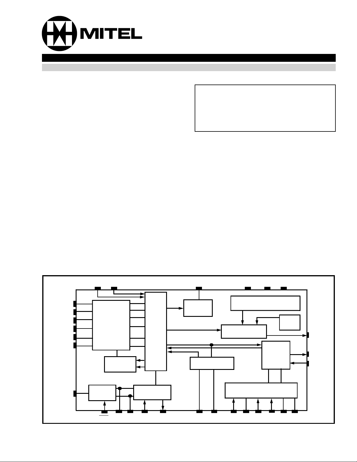
VEE
AGND
2W/4W
conversion
GTX0
GTX1
Ring
Filter
SHK
N1
N2
TX
RING
RF1
RF2
TIP
TF1
TF2
TRD
LGND
VBat VDD
Matched
Feed
Resistors
Test Relay
Driver
TRC
Auto Ring
Trip
RGND
VRLY
Driver
Circuitry
and
Speech
Circuit
Ring Relay
Driver
RNGC
RRD
LCA
Loop
Current
Set
Impedance
Z1
Network
Switch-Hook
Detect
GRX0
GRX1Z2
Switch-Hook
Threshold Set
Gain Adjust
RX
Figure 3 - Functional Block Diagram
2-159

MH88620IN Preliminary Information
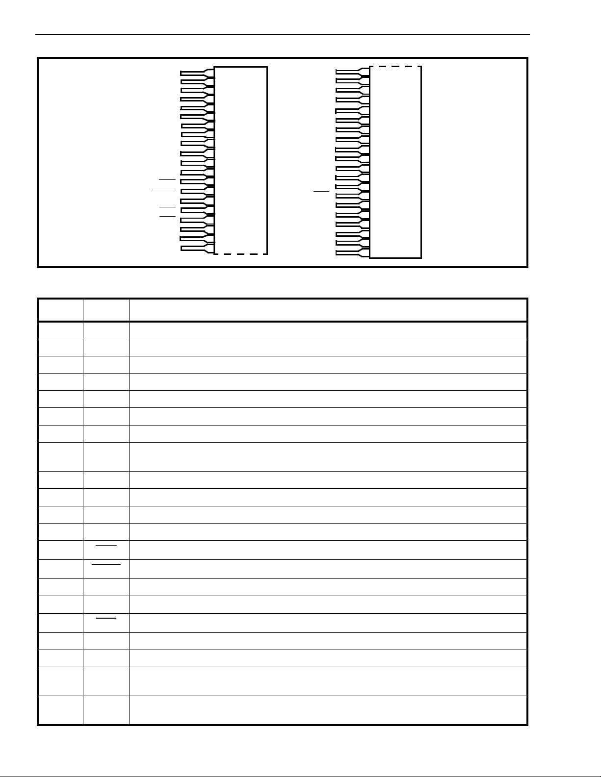
TIP
RING
TF1
TF2
RF1
RF2
LGND
LCA
VBAT
NC
RGND
VRLY
RRD
RNGC
NC
TRD
TRC
AGND
NC
N1
1
2
3
4
5
6
7
8
9
10
11
12
13
14
15
16
17
18
19
20
N2
NC
Z1
Z2
TX
RX
GTX0
GTX1
GRX0
GRX1
NC
NC
NC
SHK
IC
IC
IC
IC
VEE
VDD
Figure 2 - Pin Connections
Pin Description
Pin # Name Description
1TIPTip Lead. Connects to the TIP lead of the subscriber line
2RINGRing Lead: Connects to the Ring lead of the subscriber line.
21
22
23
24
25
26
27
28
29
30
31
32
33
34
35
36
37
38
39
40
3TF1Tip Fee d 1: Access point for balanced ringing. Normally connects to TF2.
4TF2Tip Feed 2: Access point for balanced ringing. Normally connects to TF1.
5RF1Ring Feed 1: Access point for balanced ringing. Normally connects to RF2.
6RF2Ring Feed 2: Access point for balanced ringing. Normally connects to RF1.
7LGNDBattery Ground. V
return path. Connected to system’s energy dumping ground.
BAT
8LCACurrent Limit Se t (Inpu t) : The current limit is set by connecting an external resistor as
shown in Table 5. For 70mA default current, this pin is tied to -5V.
9V
Battery Voltage: Typically -48V dc is applied to this pin.
Bat
10 RS1 Ring Sense Resistor Conn ectio n 1. See Figure 7a.
11 RGND Ring Driver Ground Con nection .
12 VRLY Relay Supply Voltage Connection
13 RRD
Ring Relay Drive (Output). Connects to ring relay coil
14 RNGC Ring Relay Control (Input)
15 RS2 Ring Sense Resistor Conn ectio n 2. See Figure 7a
16 TRD Test Relay Drive (Output): Connects to test relay coil.
17 TR C
18 AGND Analog Ground: V
Test Relay Con trol (Input).
and V
DD
return path
EE
.
19 NC No Connection: Reserved.
20 N1 Network Balan ce Nod e 1. An external network balance impedance can be connected
between N1 and AGND. See Fig 4. for compl ex imped ances. N2 no connecti on.
21 N2 Network Balance Node 2. See Fig 4. N2 connects to GND for 600Ω balance. N1 no
connection.
2-160

Preliminary Information MH88620IN
Pin Description (Continued)
Pin # Name Description
22 NC No Connection. Reserved
23 Z1 Line imp eda nce Nod e 1. Normally connect s to Z2. See Fig. 3.
24 Z2 Line impedance Nod e 2. Normally connect s to Z1. See Fig 3.
25 TX Transmit (Output)
26 RX Receive (Input). 4-wire (AGND) referenced audio inpu t.
27 GTX0 Transmit Gain Node 0. Connects to GTX 1 for 0dB transmit gain.
28 GTX1 Transmit Gain Node 1. Connects to a resistor to AGND for transmit gain adjustment.
29 GRX0 Recei ve Gai n Nod e 0. Connects to GRX1 for 0dB gain
30 GRX1 Receive Gain Node 1. Connect to a resistor to AGND for receive gain adjustment
31 NC No Connection. Reserved
32 NC No Connection. Reserved.
33 NC No Connection. Reserved.
34 SHK
35.38 IC Internal Con necti on.
39 VEE Negative Supply Voltage. -5V dc.
40 VDD Positive Supply voltage. +5V dc
Off-Hook Indication (Outp ut). A logic low output indicates when the sub scriber
equipment has gone Off-Hook.
. 4-wire (AGND) referenced audio output .
2-161

MH88620IN Preliminary Information
Absolute Maximum Ratings * All voltages are with respect to GNDA unless otherwise stated.
Parameter Symbol Min Max Units
1 Supply Voltages LGND -V
V
GND - V
2 Storage Temperature T
* Exceeding these values may cause permanent damage. Functional operation under these conditions is not implied.
DD -
Bat
GND
EE
S
-40 +125 °C
65
6
6
Recommended Operating Conditions† - Voltages are with respect to GNDA unless otherwise stated.
Characteristics Sym Min Typ* Max Units Comments
1 Operating Temperature T
2 Supply Voltages V
* Typical figures are at 25°C and are for desi gn aid only; not guarantee d and not subje ct to producti on testing.
† Voltages specified are with respect to LGND.
V
V
OP
Bat*
DD
EE
070°C
-44
4.75
-4.75
-48
+5.0
-5.0
-60
5.25
-5.25
V
V
V
DC Electrical Characteristics*
‡
Characteristics Sym Min Typ
1
Operating Loop Current
I
Loop
17
16
Max Units Test Comments
70 mA
mA
mA
= 0Ω, LCA = -5V
R
Loop
1500Ω
2000Ω V
Bat
V
V
V
= -48V
Variation in Loop current
from nominal
2
Operating Current
Power Dissipation
SHK
3
Low Level Output Voltage
High Level Output Voltage
4
RNGC
TRC
5
Low Level Input Voltage
High Level Input Voltage
Low Level Input Current
High Level Input Current
* DC Electrical Characteristics are over recommended operating conditions unless otherwise stated.
‡ Typical figures are at 25°C with nom inal ±5 V supplie s and are for desig n aid only.
I
Loop
I
Bat
I
DD
I
EE
PDo
PD1
V
OL
V
OH
V
IL
V
IH
I
IH
I
IL
±2
2
15
15
2
250
0.5 V
3.7
0.8 V
2.4
20
20
mA
mA
mA
mA
W
mW
V
V
µA
µA
= Open (On-hook)
R
Loop
On-Hook or Off-Hook
On-Hook or Off-Hook
Active
Stand-by/I dle
= 400µ A
I
OL
I
= 40µ A
OH
VIH = 5.0V
= 0.0V
V
IL
2-162

Preliminary Information MH88620IN
AC Electrical Characteristics*
1
1
8
12
‡
Max Units Test Comments
R
RMS
= 1400Ω
Loop
Term. 6.8µF +200Ω
V
2.0
8
V
RMS
dB
msec
= -48V
Bat
T-R load = 10Ωk min.
Dial Pulse Detection
msec
dB
dB
dB
dB
dB
dB
300-500Hz
500-2500Hz
2500-3400Hz
2000Hz, 1000Hz
2000Hz, 3000Hz
3400Hz
dBrnC
dBrnC
Characteristics Sym Min Typ
1
Analog Tx Gain (T-R to TX) 0 dB Externally adjustable
2
Analog Rx G ain (RX to T-R) 0 dB Externally adjustable
3
Ringing Capability 25 V
4
On-hook Transmission
Signal input lev el
Gain 4
5
SHK Rise Time
Fall time
6
2 Wire Termination Impedance 600 Ω Adjusta ble
7
Off-Hook Detect Threshold 10 mA
8
2-Wire Return Loss
600Ω at T-R
t
R
t
F
20
26
20
9
Longitudinal Balance
Longitudinal to Metallic 58
55
53
10
Longitudinal Current Capabilit y 40 mA 20mA per lead
11
Idle Channel Noise
12
Transhybrid Loss
Rx to T-R
T-R to Tx
N
CR
N
CX
THL
Tx gain 0dB
Rx gain 0dB
16
20
16
13
Analog Signal Overload Level at
TIP and RING 4 dBm
14
Ringing Signal Voltage 70 80 90 V
15
Ringing Frequency 2 0 25 30 Hz
16
Ring Trip Delay 100 ms
17
Absolute Gain variation -25 0 +. 25 dB 0dB m at T-R, 1kHz
18
Relative Gain, reference to 1kHz -2 0 +.2 dB 300-3400Hz
19
Power Supply Rejection Rat io
V
BAT
V
DD
V
EE
* AC Electrical Characteristics are over Recommended Operating Conditions unless otherwise stated.
‡ Typical figures are at 25C with nominal ± 5V supplies and are for design aid only.
Note: Test Conditions use a transmit and receive gain set to 0dB default and a Z
“Ref” indicates reference impedance which is equivalent to the termination impedance.
“Net” indicates ne two rk bala nce impe dance.
PSRR
24
24
24
30
30
30
value of 600Ω unless otherwi se sta ted.
in
dB
dB
dB
300-500Hz
500-2500Hz
2500-3400Hz
T-R = 900Ω
= -48V
V
BAT
RMS
dB 1kHz, 100mVpp
2-163
 Loading...