MITEL MH88620BR Datasheet

MH88620BR
C.O. SLIC
Preliminary Info rm atio n
Features
• 900 ohm inp ut imp eda nce
• Externally s electa ble net work ba lanc es
• Transformerless 2-4 wire conversion
• Programmab le c onsta nt resis tan ce feed
• Off-Hook and Dial pulse detection
• High immunity to externally induced longitudinal
currents
• Auto ring trip
• On-hook tran smissi on (A NI) cap ability
• Minimum p rotecti on circ uitry requi red
• Compatible with require men ts of TEL EBR AS
DOC/FCC, CSA/UL, CCITT
• Excellent power dissipation (SIL vertical
mountin g)
Applications
• On/Off-Premise PBX Line Cards
• Central Offic e Line C ard s
ISSUE 3 April 1995
Ordering Information
MH88620BR 40 Pin SIL Package
0°C to 70°C
Descript io n
The Mitel MH88620BR SLIC provides all of the
functions required to interface 2-wire off premise
subscriber loops to a serial TDM, PCM, switching
network of a modern PBX. The MH88620BR is
manufactured using thick film hybrid technology
which offers high voltage capability, reliability and
high density resulting in significant printed circuit
board area savings. A complete line card can be
implemented with very few external components.
V
AGND
EE
2W/4W
conversion
GTX0GTX1RX
Ring
Filter
TX
SHK
N1
N2
RING
RF1
RF2
TIP
TF1
TF2
TRD
V
Bat
Matched
Resistors
Test Relay
Driver
TRC
LGND
Feed
Auto Ring
Trip
RGND
VRLY
Driver
Circuitry
and
Speech
Circuit
Ring Relay
Driver
RNGC
RRD
LCA
Loop
Current
Set
Impe dance
Network
Z2Z1
Switch-Hook
Detect
GRX1
GRX0
V
DD
Switch-Hook
Thre sh ol d Set
Gain Adjust
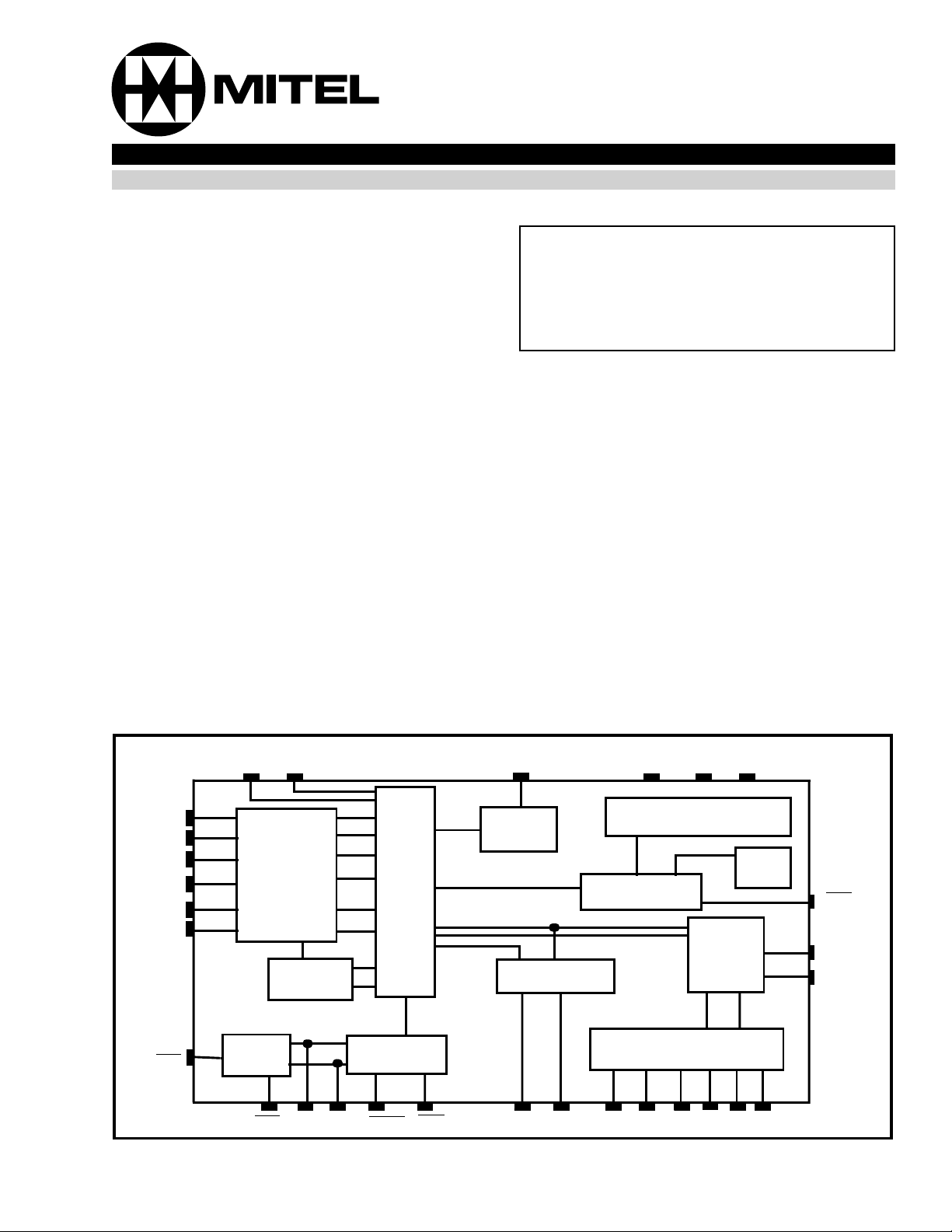
Figure 1 - Functional Block Diagram
2-145

MH88620BR Preliminary Information
TIP
RING
TF1
TF2
RF1
RF2
LGND
LCA
VBA T
IC
RGND
VRLY
RRD
RNGC
REVC
ESI
ESE
AGND
NATT
N1
1
2
3
4
5
6
7
8
9
10
11
12
13
14
15
16
17
18
19
20
N2
NC
Z1
Z2
TX
RX
GTX0
GTX1
GRX0
GRX1
NC
NC
NC
SHK
IC
IC
IC
IC
VEE
VDD
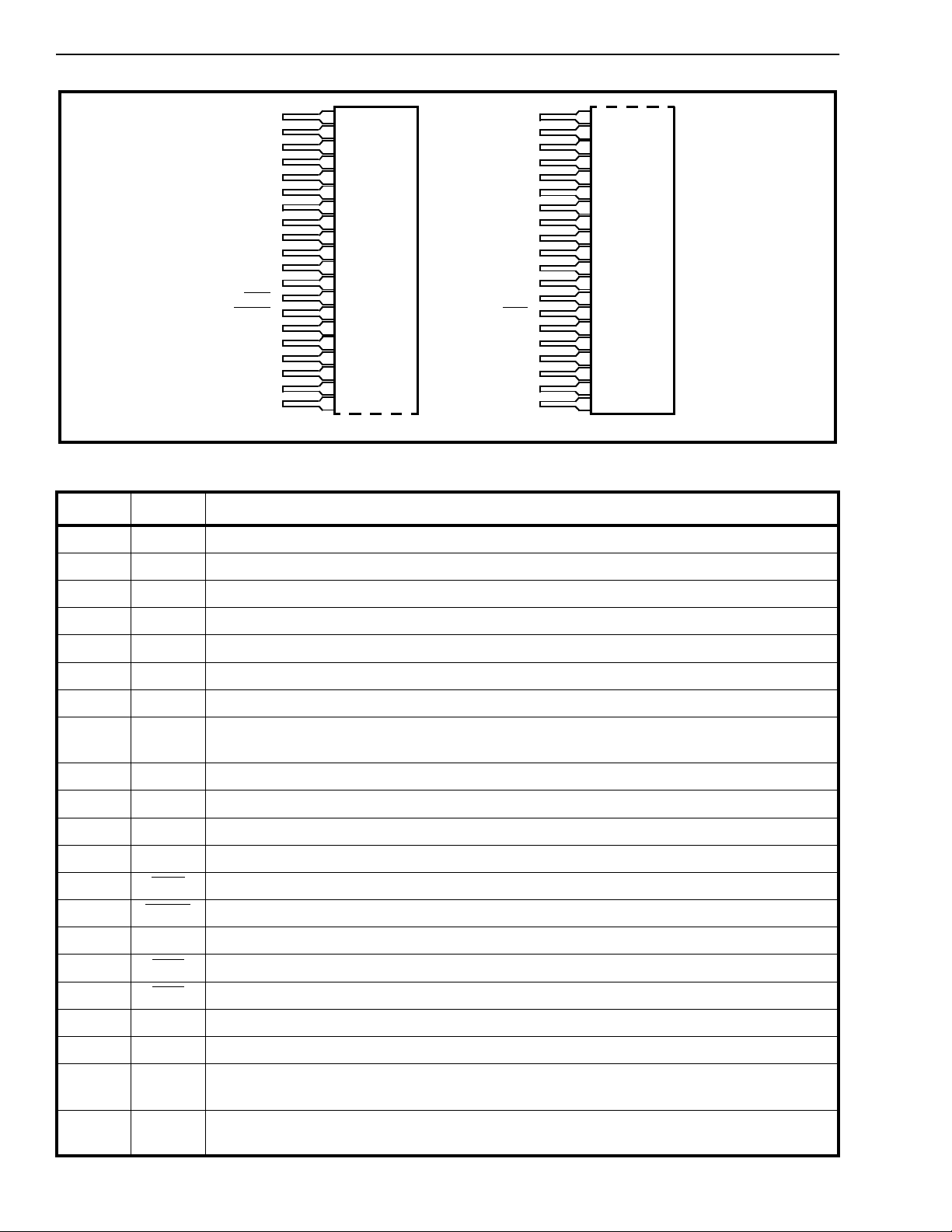
Figure 2 - Pin Connections
Pin Description
Pin # Name Description
1TIPTip Lead. Connect s to the TIP lead of the subscriber line.
21
22
23
24
25
26
27
28
29
30
31
32
33
34
35
36
37
38
39
40
2 RING Ring Lead: Connects to the Ring lead of the subscriber line.
3TF1Tip Feed 1: Access point for balanced ringing. Normally conne cts to TF2.
4TF2Tip Feed 2: Access point for balan ced ringing. Normally connects to TF 1.
5RF1Ring Feed 1: Access point for balanced ringing. Normally connects to RF2 .
6RF2Ring Feed 2: Access point for balanced ringing. Normally connects to RF1 .
7LGNDBattery Ground. V
return path. Connected to system’s energy dumping ground.
Bat
8LCACurren t Limit Set (In put): The current limit is set by connecting an external resistor as
shown in Table 5. For 70mA default current, this pin is tied to -5V.
9V
Bat
Battery Vo ltage: Ty pi cally -48V dc is applied to this pin.
10 NC No Connection: Reserved.
11 RGND Ring Driver Ground Connection.
12 VRLY Relay Supply Voltage Connection.
13 RRD
14 RNGC
Ring Relay Dri ve (Ou tp ut). Connects to ring relay coil.
Ring Relay Co ntro l (Input) .
15 NC Reserved. No Connection.
16 TR D
17 TR C
Test Relay Drive (Output ): Connects to test relay coi l.
Test Relay Control (Inp ut).
18 AGND Analog G r oun d: V
and V
DD
return path.
EE
.
19 NC No Connection: Reserved.
20 N1 Network Balance Node 1. An external network balance impedance can be connected
between N1 and AGND. See Fig 4. For complex impedances N2 no connection.
21 N2 Network Balance Node 2. An external network balance impedance can be connected
between N2 and AGND. See Fig 4 N2 connects to GND for 900Ω balance.
2-146

Preliminary Information MH88620BR
Pin Description (Continued)
Pin # Name Description
22 NC No Connection. Reserved.
23 Z1 Line impedance Node 1. Normally connects to Z2. See Fig. 3.
24 Z2 Line impedance Node 2. Normally connects to Z1. See Fig 3.
25 TX Transmit (Output)
26 RX Receive (Input). 4-wire (AGND) referenced audio input.
27 GTX0 Transmit Gain Node 0. Connects to GTX1 for 0dB transmit gain.
28 GTX1 Transmit Gain Node 1. Connects to a resistor to AGND for transmit gain adjustment .
29 GRX0 Receive Gain Node 0. Connects to GRX1 for 0dB gain.
30 GRX1 Receive Gain Node 1. Connect to a resistor to AGND for receive gain adjustme nt.
31 NC No Connection. Reserved.
32 NC No Connection. Reserved.
33 NC No Connection. Reserved.
34 SHK
35.38 IC Internal Connection.
39 VEE Negati ve Su pp ly Voltage. -5V dc.
40 VDD Positive Supply voltag e. +5V dc
Off-Hook Indicati on (Outpu t). A logic low output indicates when the subscriber
equipment has gone Off-Hook.
. 4-wire (AGND) referenced audio output.
2-147

MH88620BR Preliminary Information
Absolute Maximum Ratings * All voltages are with respect to GNDA unless otherwise stated.
Parameter Symbol Min Max Units
1 Supply Voltages LGND -V
V
GND - V
2 Storage Temp eratu re T
* Exceeding these values ma y cause perm anen t dama ge. Functi onal operati on und er these cond ition s is not implied.
DD -
Bat
GND
EE
S
-40 +125 °C
65
6
6
Recommended Operating Conditions† - Voltages are with respect to GNDA unless otherwise stated.
Characteristics Sym Min Typ* Max Units Comments
1 Operating Temperature T
2 Supply Voltages V
* Typical figures are at 25°C and are for design aid only; not guaran teed an d not subject to producti on testing .
† Voltages specified are with respect to LGND.
OP
Bat
V
DD
V
EE
V
RLY
070°C
-44
4.75
-4.75
-48
+5.0
-5.0
5
70
-60
5.25
-5.25
V
V
V
V
DC Electrical Characteristics*
‡
Characteristics Sym Min Typ
1
Operating Loop Current
I
Loop
17
16
Max Units Test Comments
70 mA
mA
mA
= 0Ω, LCA = -5V
R
Loop
1500Ω
2000Ω V
Bat
V
V
V
= -48V
Variat ion in Loop Current
I
Loop
±2
from nominal
2
3
SHK
4
RNGC
TRC
5
* DC Electrical Characteristics are over recommended operating conditions unless otherwise stated.
‡ Typical figures are at 25°C with nom inal ±5 V supplie s and are for desig n aid only.
Operating Current
Power Dissipation
Low Level Input Voltage
High Level Input Voltage
Low Level Input Voltage
High Level Input Voltage
Low Level Input Current
High Level Input Current
I
Bat
I
DD
I
EE
PDo
PD1
V
OL
V
OH
V
IL
V
IH
I
IL
I
IH
2
15
15
2
250
0.5 V
3.7
0.8 V
2.4
20
20
mA
mA
mA
mA
W
mW
V
V
µA
µA
= Open (On-hook)
R
Loop
On-Hook or Off-Hook
On-Hook or Off-Hook
Active
Stand-by/I dle
= 400µ A
I
OL
I
= 40µA
OH
VIL = 0.0V
= 5.0V
V
IH
2-148

Preliminary Information MH88620BR
AC Electrical Characteristics*
Characteristi cs Sym Min Typ
1
Analog Tx Gain (T-R to TX) 0 dB Externally adjusta ble
2
Analog Rx Gain (RX to T-R) 0 dB Ex ter nally a djust abl e
3
Ringing Capability 25 V
4
On-hook Transmission
Signal input level
Gain 4
5
SHK Rise Time
Fall time
6
2 Wire Termination Im peda nce 900 Ω A djust able
7
Off-Hook Detect Threshold 10 mA
8
2-Wire Return Loss
Ω at T-R
900
Zin = 900Ω
t
R
t
F
20
26
20
‡
Max Units Test Com m en ts
R
RMS
Loop
= 1400Ω
Term. 6.8µF +200Ω
V
2.0
8
1
1
V
RMS
dB
msec
msec
dB
dB
dB
= -48V
Bat
T-R load = 10Ωk min.
Dial Pulse Detection
300-500Hz
500-2500Hz
2500-3400Hz
900Ω + 2.16µF at T-R
Zin = 900Ω
14
18
14
9
Longitudinal Balance
Longitudinal to Metallic 58
55
53
10
Longitudinal Current Capabil ity 40 mA 20mA per lead
11
Idle Channel Noise
8
12
12
Transhybrid Loss
Tx gain 0dB
Rx gain 0dB
Rx to T-R
T-R to Tx
N
CR
N
CX
THL
16
20
16
13
14
Analog Signal Overload Level at
TIP and RING 4 dBm
15
Ringing Signal Voltage 70 80 90 V
16
Ringing Frequency 20 25 30 Hz
17
Ring Trip Delay 100 ms
18
Absolute Gain variation -25 0 +.25 dB 0dBm at T-R, 1kHz
19
Relative Gain, reference to 1kHz -2 0 +.2 dB 300-3400Hz
20
Power Supply Rejection Ratio
V
Bat
V
DD
V
EE
* AC Electrical Characteristics are over Recommended Operating Conditions unless otherwise stated.
‡ Typical figures are at 25°C with nomina l +
Note: Test Conditions use a transmit and receive gain set to 0dB default and a Z
“Ref” indicates reference impedance which is equivalent to the termination impedance.
“Net” indicates ne two rk bala nce impe dance.
5V supplies and are for design aid only.
PSRR
24
24
24
30
30
30
value of 900Ω unless otherwi se stated .
in
dB
dB
dB
dB
dB
dB
300Hz
600-2000Hz
3400Hz
2000Hz, 1000Hz
2000Hz, 3000Hz
3400Hz
dBrnc
dBrnc
dB
dB
dB
300-500Hz
500-2500Hz
2500-3400Hz
T-R = 900Ω
= -48V
V
Bat
RMS
dB 1kHz, 100mVpp
2-149
 Loading...