MITEL MH88600 Datasheet

MH88600
Global SLIC
Preliminary Information
Features
• Programmable line impedance matching
• Internal complex i mp edance netw ork s
• Transformerless 2-4 wire conversion
• Programmable transmit/receive gain
• Accomm odat es worl dw ide trans miss ion
standards
• Opera tes with a wide range of ba tte ry volt ages
• Adjustab le c onsta nt curre nt ba ttery feed
• Overvol tag e and sho rt circu it pro tectio n
• Switch hoo k an d groun d bu tton de tectio n
• Ring tri p filte r and rel ay d river
• Low pow er co nsump tion
• High power dissipation capability during fault
conditions
Applications
Line interface for:
• PABXs
• Contr ol Sys tems
• Key Telephone Sy stems
• Central Office Equipment
ISSUE 7 April 1995
Ordering Information
MH88600 40 Pin DIL Hybrid
0°C to 70°C
Description
The MH88600 is a SLIC (Subscriber Line Interface
Circuit) which provides all of the BORSCH functions
of Battery Feed, Overvoltage Protection, Ringing
Feed, Line Supervision and 2-4 Wire Hybrid
conversion. In addition, the device matches the
many different line impedances specified by
regulatory authorities of around the world.
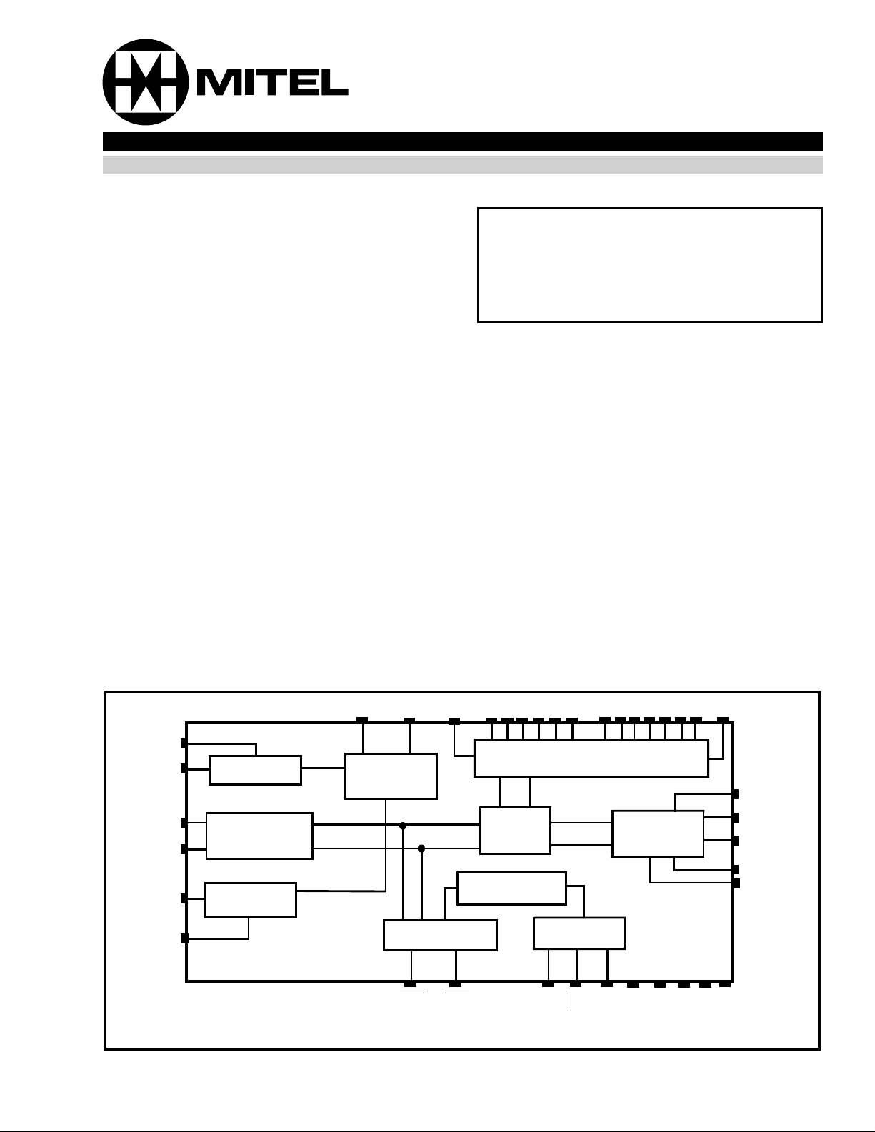
TF1
TF2
TIP
RING
RF1
RF2
Tip Drive
Over Voltage &
Short Circuit
Protection
Ring Drive
VREF
Constant
Current
Battery Feed
LCA
ZN14
Line Supervision
EGB
SHK
ZN13.................ZN8
Impedance Matchi ng Network
2-4 Wire
Hybrid
Circuit
Ring Trip Filter
Relay Driver
RC
ZN7.....................ZN1
RD
Figure 1 - Functional Block Diagram
Gain Adjust
VRR
GNDA
VDD
ZN0
PG2
PG4
TX
PG3
PG1
VEE
Vbat
GNDBat
2-83

MH88600 Preliminary Information
40
ZN14
39
38
37
36
35
34
33
32
31
30
29
28
27
26
25
24
23
22
21
ZN13
ZN12
ZN11
ZN10
ZN9
ZN8
ZN7
ZN6
ZN5
ZN4
ZN3
ZN2
ZN1
TX
PG3
PG1
PG2
PG4
ZN0
Pin Description
TIP
IC
RC
RD
2
3
4
5
6
7
8
9
10
11
12
13
14
15
16
17
18
19
20
VBat
RF1
RF2
RING
GNDBat
TF2
TF1
GNDA
VEE
VDD
VRR
LCA
SHK
EGB
VRef
Figure 2 - Pin Connections
Pin # Name Description
1 No pin at this location.
2V
Bat
Battery Supply Voltage (Negati ve).
3RF1Ring Fe e d ( 1 ): Conne ct to relay contact. See Figures 6 & 7.
4
RF2
Ring Fe e d ( 2 ). Connect to relay contact. See Figu res 6 & 7.
5 RING Connects to the “Ring” or “B” lead of the telephone line.
6 TIP Connects to the “Tip” or “A” lead of the telephone line.
7I/CInternal Connection .
8GND
Battery Supply Ground (Positive ): Connect to System Ground
Bat
9TF2Tip Feed (2). Connect to TF1 for unbalanced ringing, see Figure 6. Connect to relay
contact for balanced ringing, see Figure 7.
10 TF1 Tip Feed (1). Connect to TF2 for unbalanced ringing, see Figure 6. Connect to relay
contact for balanced ringing, see Figure 7.
11 GNDA Analog Ground: Normally connected to System Ground.
12 V
13 V
14 V
EE
DD
RR
Negative Power Supp ly Voltage: Normally -5V.
Positive Pow er Su pp ly Voltage: Normally +5V.
Ringing Relay Cl am p Di ode : Connect to relay coil and to relay supply voltage
(Positive). For +5V relay, connect to VDD.
15 RC Ring Control (Input): A logi c hig h will activat e the Ri ng Relay D rive if SHK is high.
16 RD
Ring Relay Drive (Outpu t ). Connect to relay coil. A logic low will activate the relay by
sinking current from VRR through the relay coil.
17 LCA Loop Current Adjust (Input): Loop current is prop ortio nal to the vol tage at this input.
Normally connected to VRef
18 SHK Switch Hook Detect (Output): A logic low indicates an off-hook condition.
19 EGB
20 V
2-84
Ref
Earth Ground Button (Output ): A logic low indicates a grounded Ring lea d condition.
Voltage Reference (Output): Normally connected to LCA for default loop current.

Preliminary Information MH88600
Pin Description (Contin ue d)
Pin # Name Description
21
ZN0
Impedance Node 0. Connect to external network for impedance (Zin) setting. See Table
2 and Figure 8.
22 PG4 Programming 4 (Input). Used for programmable gain and fo r default gain. Used as 4-
Wire Receive Input for default gain. See Table 3 and Figure 4 and 5.
23 PG2 Programming 2 (Input). U sed for programmab le gain. Used with resistor for 4-Wire
Receive Input. See Table 3 and Figure 4.
24 PG1 Programming 1 (Input). Used for programmable gain. See Table 3 and Figure 4.
25 PG3 Programming 3 (Input). Used for programmable gain and for default gain. See Table 3
and Figure 4 and 5.
26 TX 4-Wire Transmit Output:
27 ZN1 Impedance Node 1: Connect to other Impedance Nodes for impe dance (Z
see Table 1. Or , connect to external network for impedance (Z
) setting, see Table 2 and
in
) setting,
in
Figure 8.
28 ZN2 Impedance Node 2: Connect to other impedances Nodes for im pedance (Zin) setting.
See Table 1.
29 ZN3 Impedance Node 3: As per ZN2. S ee Table 1.
30 ZN4 Impedance Node 4: As per ZN2. S ee Table 1
31 ZN5 Impedance Node 5: As per ZN2. S ee Table 1
32 ZN6 Impedance Node 6: As per ZN2. S ee Table 1
33
ZN7
Impedance Nod e 7: As per ZN2. See Table 1
34 ZN8 Impedance Node 8: As per ZN2. S ee Table 1
35 ZN9 Impedance Node 9: As per ZN2. S ee Table 1
36 ZN10 Impedance Nod e 1 0: As per ZN2. See Table 1
37 ZN11 Impedance Nod e 11: As per ZN2. See Table 1
38 ZN12 Impedance Nod e 1 2: As per ZN2. See Table 1
39 ZN13 Impedance Nod e 1 3: As per ZN2. See Table 1
40 ZN14 Imp eda nce Nod e 14 : Connect to external net work for impedance (Z
Table 2 and Figure 8.
) setting. See
in
.
2-85

MH88600 Preliminary Information
Functional Description
The BORSH Functions
The MH88600 performs all of the BORSH functions;
Battery Feed, Overvoltage Protection, Ringing,
Supervision and Hybrid.
Battery Feed
The MH88600 provides the loop with constant DC
current to power the telephone set. The voltage
(negative) applied at the LCA pin determines the
magnitude of the lop current.
I
= 3.731 x VLCA mA (±2mA)
Loop
Either the internal (V
voltage reference may be used to set the loop
current.
Overvol tage P rote ction
The MH88600 is protected from short term (20ms)
transients (+250V) between Tip and Ring, Tip and
ground, and Ring and Ground. However, additional
protection circuitry may be needed depending on the
regulatory requirements which must be met.
Normally, simple external shunt protection as shown
in Figures 6,7 and 8 is all that is required.
Ringing
The MH88600 has the capability to accommodate
both balanced and unbalanced ringing sources.
Refer to Figure 7 for the Balanced Ringing Circuit
and Figure 6 for the Unbalanced Ringing Circuit.
Supervision
The MH88600 is capable of detecting both Ground
Button and Switch Hook conditions. The Ground
Button detection (a logic low at the EGB
operates when an imbalance in Tip and Ring DC
current exceeds an internal threshold level caused
by a grounded Ring Lead. Use of the EGB
restricted to the off-hook condition of the telephone.
The Switch Hook detection operates (a logic low at
the SHK
an interna l th reshold level .
output) when the DC loop current exceeds
) or an external negative
Ref
output)
output is
Hybrid
The 2-4 Wire Hybrid circuit separates the balanced
full duplex signal at Tip and Ring of the telephone
line into receive and transmit ground referenced
signals at RX (receive) and TX (transmit) of the
SLIC. The Hybrid also prevents the input signal at
RX from appearing at TX. The degree to which the
Hybrid prevents the RX signal from appearing at TX
is specified at transhybrid loss.
Tip-Ring Drive Circuit
The audio input ground referenced signal at RX is
converted to a balanced output signal at Tip and
Ring. The output signal consists of the audio signal
superimposed on the DC Battery Feed Constant
Current. The Tip-Ring Drive Circuit is optimised for
good 2-Wire longitudinal balance.
Short Circuit Protection
The MH88600 is protected from long term (infinite)
short circuit conditions occurring between Tip and
Ring, Tip and Ground, Ring and Ground, and Ring
and Batte ry. The current is lim ited to the sam e v alue
as the Constant Current Battery Feed.
Programmable Line Impedanc e
The MH88600’s Tip-Ring (Zin) impedance can be
matched to the different impedances specified by
different telephone administrations worldwide. This
is accomplished by either linking specific pins as
specified in Table 1, or by adding external
components as shown in Figure 8 and Table 2.
Programmable Transmit & Receive G ain
Transmit gain (TX to Tip-Ring) and Receive Gain
(Tip-Ri ng to RX) c an be prog ram med by conn ectin g
external resistors as indicated in Figure 4 and Table
3. Alternatively, the default Receive Gain of -4d Band
Transmit Gain of +4dB can be obtained by
connecting pins as shown in figure 5 and Table3.
Note that RX is not a pin on the SLIC. The RX
terminal will be either PG4 or the connection to the
receive gain programming resistor RRX shown in
Figure 4 and Figure 5.
The Ring Trip Detection Circuit prevents false offhook detection due to the current associated with the
AC ringing voltage and also due to the large current
transients when the ring voltage is switched in and
out. In addition , th e circu it pr ev e nt s con ne c ti on of the
ringing source during off-hook conditions.
2-86

Preliminary Information MH88600
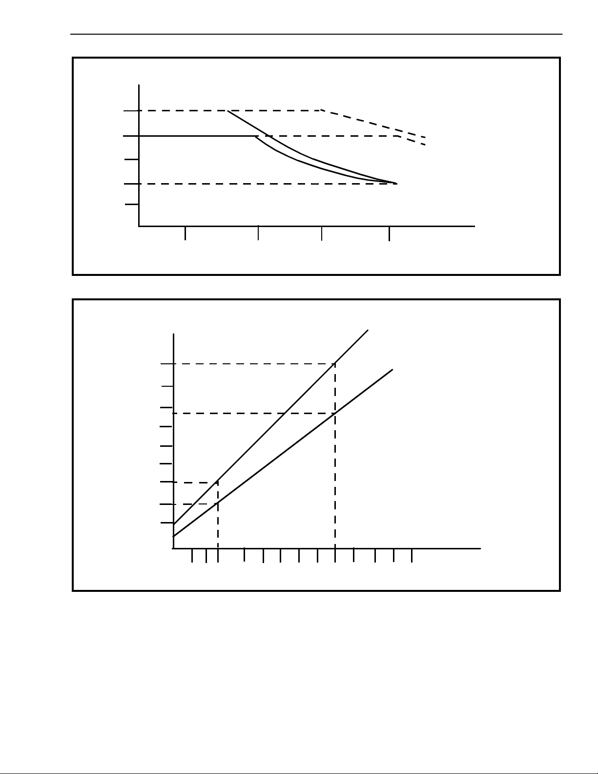
Loop Current (mA)
25
20
15
Loop Detect Threshold
10
5
Maximum Loop Length (Ω)
2000
VBat = -24V VBat =-48V
VBat = -24V
500
1000 1500
VBat = -48V
2000
Figure 3a - Loop Current vs.Maximum Loop Current
ILoop = 20mA
Maximum
Loop
Length (Ω)
1800
1600
1400
1200
1000
800
600
400
200
ILoop = 25mA
64
16
20
24
28
32
36
40
44
48
52
56
60
Figure 3b - Maxim um L oop L ength vs Batt ery vo ltag e
VBAT (V)
2-87
 Loading...