

Page 1

&KDSWHU#7 23(5$7,21# 7+(25<
&RQWHQWV
714#(OHFWURSKRWRJUDSKLFV#V\VWHP/#SDJH#705
(OHFWURSKRWRJUDSKLF#V\VWHP/#SDJH#705
$PRUSKRXV0VLOLFRQ#GUXP/#SDJH#705
&KDUJLQJ#WKH#GUXP/#SDJH#706
7RQHU/#SDJH#707
([SRVXUH/#SDJH#707
6FDQQHU#XQLW/#SDJH#708
6FDQQLQJ#ODVHU/#SDJH#70:
'HYHORSPHQW/#SDJH#70:
'HYHORSLQJ#UROOHU#ELDV/#SDJH#70;
7RQHU#VHQVRU/#SDJH#70<
7UDQVIHU/#SDJH#70<
)XVLQJ/#SDJH#7043
'UXP#FOHDQLQJ#DQG#HUDVLQJ#VWDWLF#FKDUJH/#SDJH#7044
7\SLFDO#SKRWR#SURFHVV#WLPLQJ#FKDUW/#SDJH#7045
715#3ULQW#WLPLQJ#FKDUWV/#SDJH#7046
716#3DSHU#IHHGLQJ#V\VWHP/#SDJH#704:
&DVVHWWH#IHHGLQJ/#SDJH#704;
0XOWL#SXUSRVH#WUD\#IHHGLQJ/#SDJH#704;
3DSHU#MDP#VHQVLQJ/#SDJH#704<
717#%DVLF#HQJLQH#IXQFWLRQV/#SDJH#7053
%DVLF#VHTXHQFH#RI#RSHUDWLRQ/#SDJH#7053
718#(QJLQH#FRQWUROOHU#V\VWHP/#SDJH#7054
)ODVK#PHPRU\/#SDJH#7054
3ULQW#GHQVLW\#FRQWURO/#SDJH#7054
+LJK0YROWDJH#JHQHUDWRU/#SDJH#7054
/DVHU#VFDQQHU#FRQWURO/#SDJH#7054
3RO\JRQ#PRWRU#FRQWURO/#SDJH#7054
6DIHW\#LQWHUORFN/#SDJH#7055
7KH#HQJLQH#JDWH#DUUD\/#SDJH#7056
3LQ#DVVLJQPHQW/#SDJH#7056
3RZHU#VXSSO\/#SDJH#7059
719#/RJLF#FRQWUROOHU#V\VWHP/#SDJH#705;
3ULQWLQJ#GDWD#SURFHVVLQJ/#SDJH#7063
6\VWHP#520/#SDJH#7063
0DLQ#5$0/#SDJH#7063
0HPRU\#FDUG#VORW#LQWHUIDFH/#SDJH#7064
2SWLRQ#LQWHUIDFH/#SDJH#7064
3DUDOOHO#LQWHUIDFH/#SDJH#7066
6HULDO#LQWHUIDFH/#SDJH#7066
(QJLQH#LQWHUIDFH/#SDJH#7066
6LJQDOV#XVHG#IRU#WKH#HQJLQH#LQWHUIDFH/#SDJH#7067
(QJLQH#LQWHUIDFH#EORFN#GLDJUDP/#SDJH#7068
Page 2

(OHFWURSKRWRJUDSKLFV#V\VWHP
714 (OHFWURSKRWRJUDSKLFV#V\VWHP
Electrophotography is the technology used in laser printing which transfers data representing
texts or graphics objects into a visibl e imag e which is developed on the photosensitive drum,
finally fusing on paper, using light beam generated by a laser diode.
The key features for the electrophotography system used in the printer are:
600 dpi resolution
•
Newly developed amorphous silicon drum with no heating device
•
Diode laser scanning
•
Mono component toner
•
(OHFWURSKRWRJUDSKLF#V\VWHP
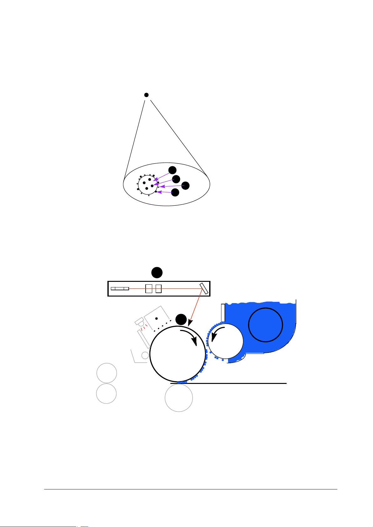
The electrophotography system of the printer performs a cyclic action made of seven steps as
diagrammed below.
)LJXUH#714 (OHFWURSKRWRJUDSKLF#F\FOH
2SHUDWLRQ#WKHRU\
([SRVXUH
&KDUJLQJ
(UDVXUH
'UXP#FOHDQLQJ
7UDQVIHU
)XVLQJ
'HYHORSPHQW
$PRUSKRXV0VLOLFRQ#GUXP
The printer uses the long lasting amorphous silicon drum. The drum surface is a composite of
five substances coated in five layers as shown in page 4-3, Figure 4.2.
4-2
)609<33
Page 3

2SHUDWLRQ#WKHRU\
(OHFWURSKRWRJUDSKLFV#V\VWHP
)LJXUH#715 $PRUSKRXV#VLOLFRQ#GUXP
D06L#OD\HU
$
%
$OXPLQXP#OD\HU
The amorphous silicon layer is photoconductive, reducing its electrical conductivity when
exposed to laser light.
$
%
'UXP#XQLW
&KDUJLQJ#WKH#GUXP
Figure below is a simplified diagram of the electrophotographics components. Charging the
drum is done by the main charger wire (in the main charger unit) marked “A” in the diagram.
$
%
)609<33
As the drum (“B” above) rotates in a “clean (neutral)” state, its photoconductive layer is given a
uniform, positive (+) electrical charge dispersed by the main charger wire (“A”).
Due to high-voltage scorotron charging, the charging wire can get contaminated by oxidization
and therefore must be cleaned periodically from time to time using the method explained on
page 3-5,
such as black streaks caused by the oxide accumulated around the charging wire.
&OHDQLQJ#WKH#SULQWHU
. Cleaning the charging wire prevents print quality problems
4-3
Page 4
2SHUDWLRQ#WKHRU\
(OHFWURSKRWRJUDSKLFV#V\VWHP
7RQHU
The toner is fed from the toner pack TK-20/H. The toner is comprised of the following substances.
6LQJOH#FRPSRQHQW#WRQHU#7.0532+
Resin
$#0#
Ferrite
%#0#
Silica
�#
Polisher
'#0#
$
%
&
'
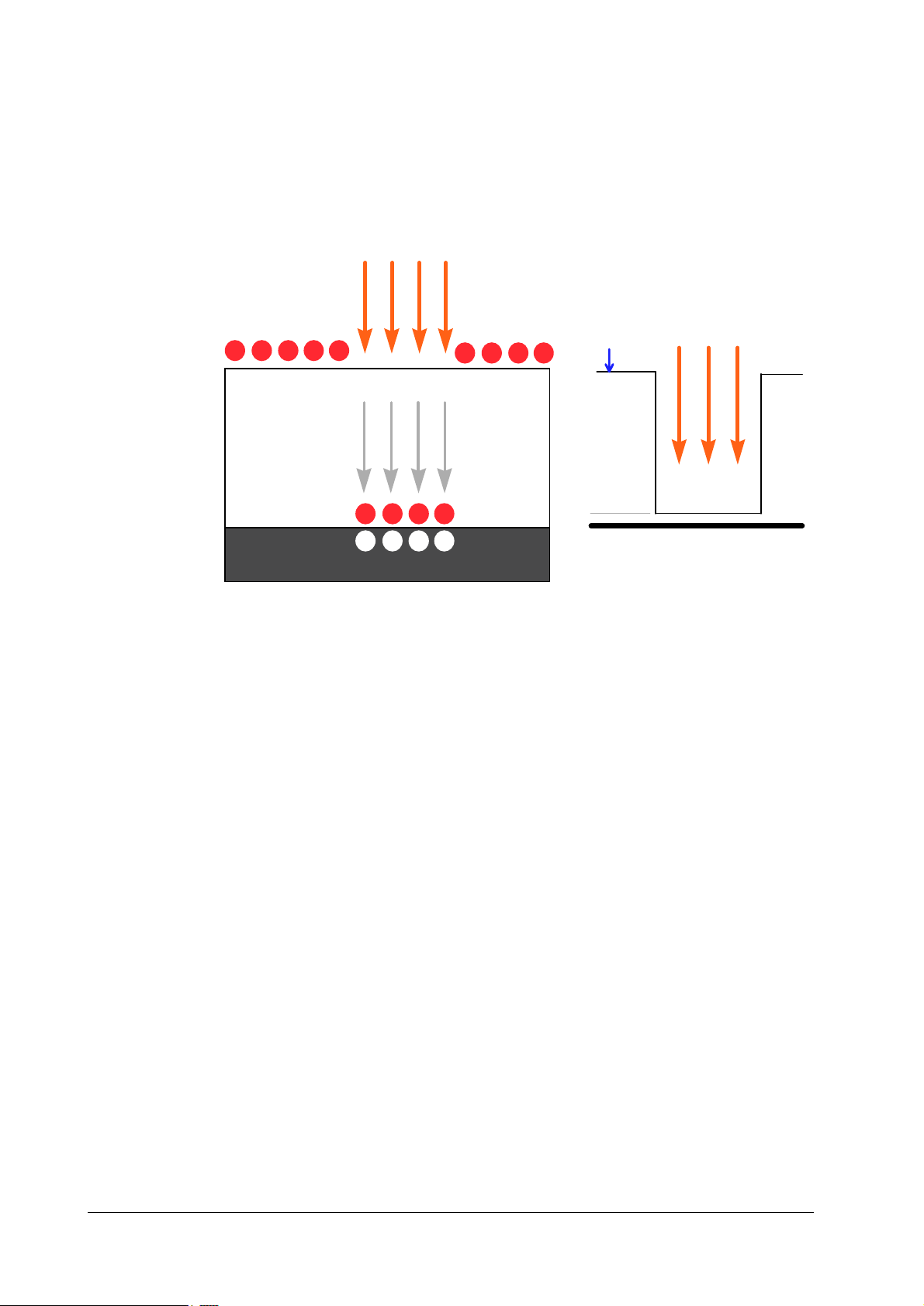
([SRVXUH
The charged surface of the drum ("B") is then scanned by the laser beam from the scanner unit
("A").
$
%
4-4
)609<33
Page 5
2SHUDWLRQ#WKHRU\
(OHFWURSKRWRJUDSKLFV#V\VWHP
The laser beam is switched on for a black dot and off for a white (blank) dot according to the
print data. Whenever it is illuminated by the laser beam, the electrical resis-tance of the photoconductor is reduced, the potential on the photoconductor is also lowered to 20 V, effectively
driving the charge through the a-Si layer down to the aluminum base.
/DVHU#EHDP
D06L#OD\HU
$OXPLQXP
3RVLWLYH#FKJ1
.#.#.#.#.
3RVLWLYH#FKJ1
1HJDWLYH#FKJ1
6FDQQHU#XQLW
The 600 dpi scanner unit includes the diode laser that produces the 670 nm wave-length laser
beam. This wavelength is specifically designed to match the photocon-ductive response of
amorphous silicon.
.#.#.#.
#
#0###0##0###0
.#.#.#.
57305939
5730593#9
53#9
3#9
/DVHU#EHDP
)609<33
4-5
Page 6
)LJXUH#716 /DVHU#VFDQQHU#XQLW
2SHUDWLRQ#WKHRU\
(OHFWURSKRWRJUDSKLFV#V\VWHP
'RZQYHUWLQJ#PLUURU
3KRWR#GLRGH
/DVHU#GLRGH
&ROOLPHWHU#OHQV
&\OLQGRULFDO#OHQV
7DE O H#71#4## )XQFWLRQ#RI#VFDQQHU#FRPSRQHQW³
&RPSRQHQW )XQFWLRQ
Laser diode Emits diffused, visible laser.
Collimeter le ns Aligns the laser be am to the cylindrical lens.
Cylindrical lens Compensates the slant angle at which the laser beam hits a polygon mirror
segment.
Polygon mirror (motor) Has six mirror segments around its oc ta gonal circumference; each mirror
corresponding to one scanned line width on the drum when laser beam
scans on it.
Primary f-theta lens See page 4-7, Figure 4.4 and below.
Secondary f-theta lens See page 4-7, Figure 4.4. The primary (above) and secondary ftheta lenses
equalize focusing distortion on the drum edges. The effective length of
line ("A," "B" below) the lase r bea m draws on the drum becomes longer
as the laser beam hits closer to the drum edges. In the figure below, dis-
tances represented by "A" and "B" are not the same (A>B) until the ftheta
lenses are provided be tween the polygon m irror and the drum (A=B) .
Diversion mirror diverts the laser beam vertica ll y onto the drum. Note the diffused la ser
beam finally pin-point s on the drum.
Protective glass Pre ve nts dust, debris, etc., from entering the scanner asse m bly.
Sensor mirror Bends the very first shot of a laser scan towards the beam detection sensor
(See next.).
Beam detector sensor When shone by the sensor mirror above, this photosensor generates a trig-
ger signal for the engine controller to start a ctivating the paper feeding
system.
&RYHU#JODVV
)0WKHWD#OHQVHV
3RO\JRQ#PLUURU2PRWRU
4-6
)609<33
Page 7
2SHUDWLRQ#WKHRU\
(OHFWURSKRWRJUDSKLFV#V\VWHP
)LJXUH#717 )XQFWLRQ#RI#)0WKHWD#OHQVHV
6HFRQG#)0WKHWD#OHQV
)LUVW#)0WKHWD#OHQV
'UXP
$
%
T
T
3RO\JRQ#PLUURU
/DVHU#GLRGH
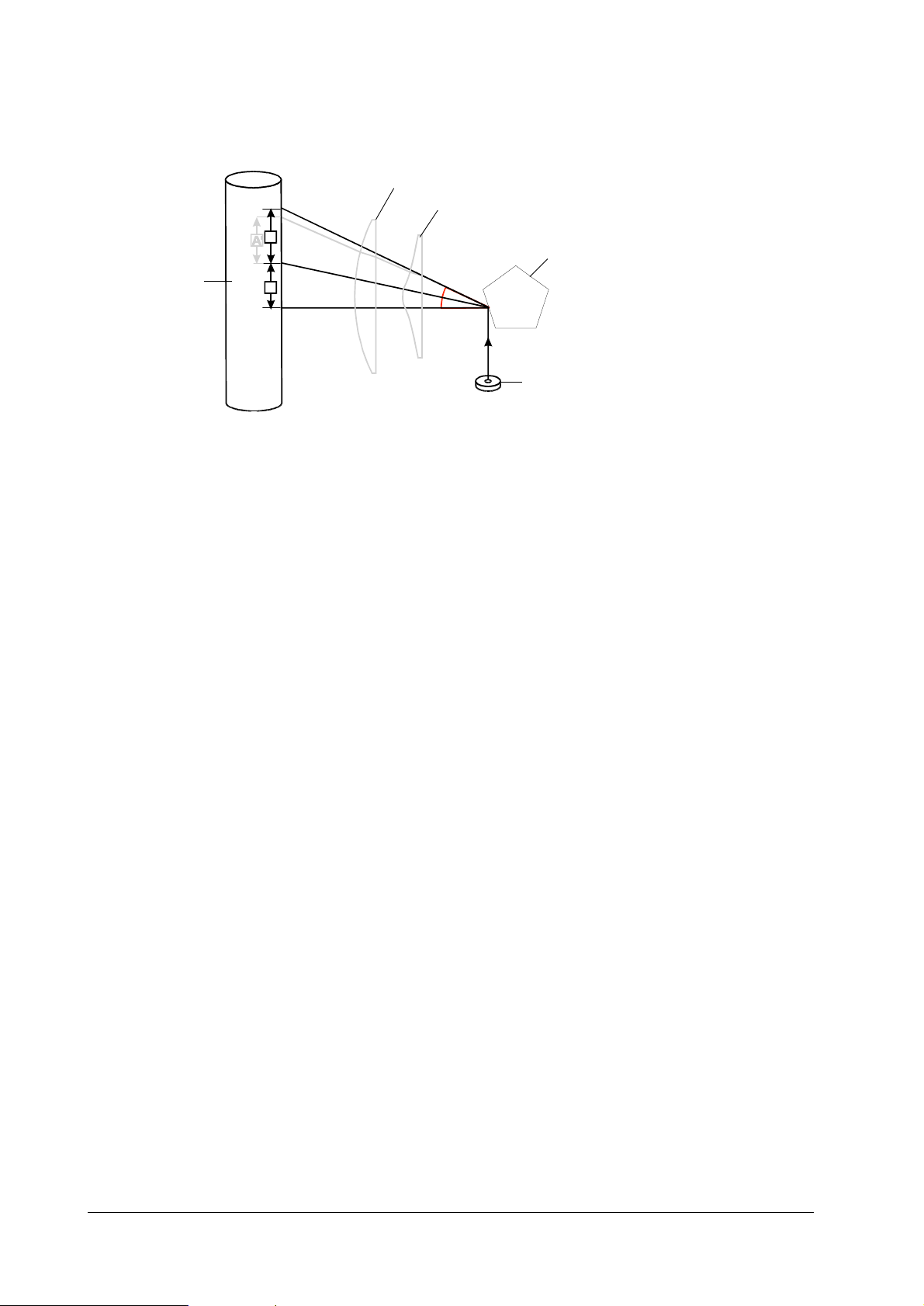
6FDQQLQJ#ODVHU
The laser beam hits one of 5 sides of t he polygo nal mi rror. As the mi rror rev olves (at the revo lution of 26600 rpm), the laser beam reflects off of it and reaches the charged drum surface in a
lengthwise manner.
A pair of (plastic) lenses provides focusing the horizontally sweeping laser beam onto the drum.
As the drum rotates, the laser beam sweeps the entire length of the drum so th at the drumís
entire circumference is exposed to the laser beam. The revolution of the polygon mirror motor
and the drum itself is timing-controlled so that each suc-cessive sweeping of the laser beam produces a 1/600 inch offset. The printer’s controller system continuously turns the laser beam on
and off to put a dot at every 1/600 inch distance horizontally. The diameter of a dot is typically
70 to 80 µm. When KIR is on, the intensity of the beam is switched in fou r deg rees compensating for the smoothed image.
Synchronizing the output data with one scanning line is achieved by the photo sensor provided
next to the first mirror. At the beginning of each laser sweeping, the beam hits the photo sensor
which in turn sends a command to the logic controller for syn-chronization.
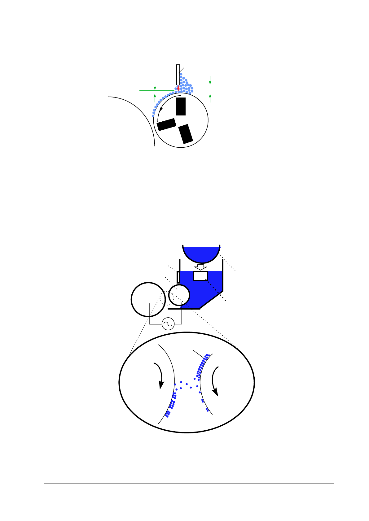
'HYHORSPHQW
The latent image constituted on the drum is developed into a visible image. The de-veloping
roller contains a 3-pole (S-N-S) magnet core and an aluminum cylinder ro-tating around the
magnet core. Toner attracts to the developing roller since it is pow-dery ink made of black resin
bound to iron particles. A magnetized blade positioned approximately 0.3 to 0.4 mm above the
developing roller constitutes a smooth layer of toner in accordance with the roller revolution.
)609<33
4-7
Page 8
2SHUDWLRQ#WKHRU\
(OHFWURSKRWRJUDSKLFV#V\VWHP
'HYHORSLQJ
EODGH
314#PP
'UXP
3160317#PP
6
0DJQHWLF
1
UROOHU
6
'HYHORSLQJ#UROOHU#ELDV
The developing roller is connected to a AC-weighted, positive DC power source. Toner on the
developing roller is given a positive charge. The positively charged toner is then attracted to the
areas of the drum which was exposed to the laser l ight. The non- exposed areas of th e drum repel
the positively-charged toner as these areas maintain the positive charge.
The developing roller is also biased with an ac potential to apply com pensation to the toner’s
attraction and repelling actions for more contrast in the development.
'HY1#EODGH
'HY1#UROOHU
'UXP
$&.'&
'UXP
7RQHU
7RQHU#VHQVRU
'HY1#UROOHU
The following diagram depicts the change in the drum surface potential during development.
The vertical distance rerepresents the depth of bias potential.
4-8
)609<33
Page 9
2SHUDWLRQ#WKHRU\
(OHFWURSKRWRJUDSKLFV#V\VWHP
%LDV#GHSWK#LV#GHWHUPLQHG#VR
DV#WR#SUHYHQW#JUD\#EDFNJURXQG1
9R DSSUR[1#573#WR#593#9
......
53#9
'HYHORSPHQW
([SRVXUH
......
'HY1#UROOHU#ELDV
4;3#9#'&.$&
7RQHU #VHQVRU
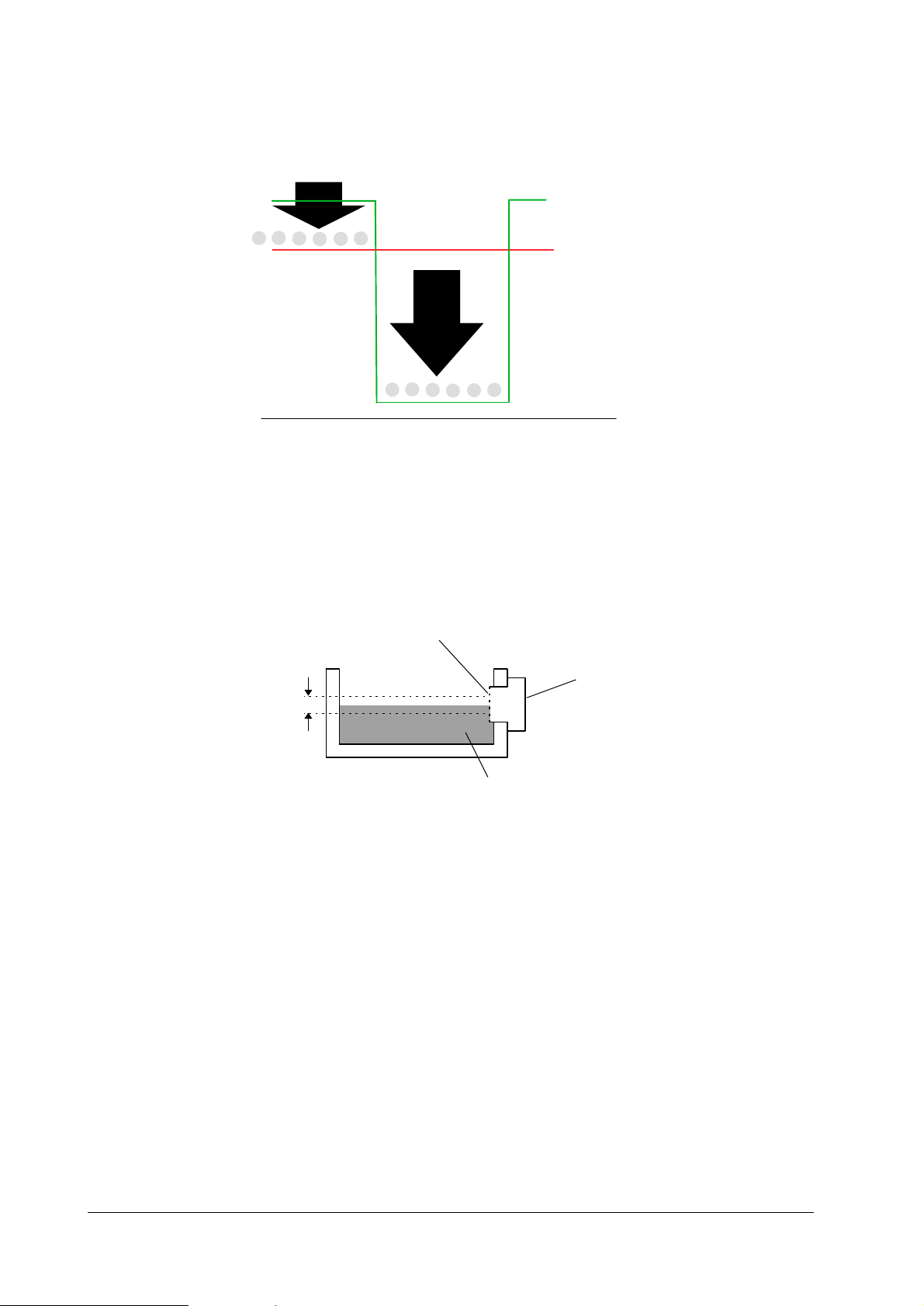
The toner replenishment sensor is provided within the developer. As the toner supply from the
toner container dwindles and the toner level low e rs in the reservoir, the sensor translates it
through its diaphragm, urging the toner motor to feed more toner.
'LDSKUDJP
6HQVRU
6HVLQJ#KHLJKW
7RQHU
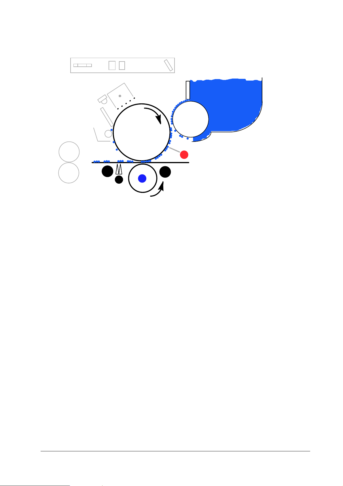
7UDQVIHU
The image developed by toner on the drum (“A” below) is transferred onto the paper using the
electric charge attraction given by the toner itself and the transfer roller (“B” below). The transfer roller is negatively biased so that the positively charged toner is attracted onto the paper
while it is pinched by the drum and the transfer roller.
The paper is automatically peeled off the drum because of the small diameter of the drum. To
prevent thin paper wrapping around the drum, the static discharger brush is provided to reduce
the attraction of the negatively charged paper to the positiv ely charged drum.
)609<33
4-9
Page 10
.
2SHUDWLRQ#WKHRU\
(OHFWURSKRWRJUDSKLFV#V\VWHP
%
.
The nominal transfer bias is set to approximately -1.80 kV (limit) with the current of 65±2 mA.
Since thicker paper (91 to 200 g/m
more bias potential for the satisfactory transferring process, the transfer bias is user-switchable
to -2.45 kV (limit) by using the printerís operator panel. Double-sided printing using a DU-25
duplexer automatically increases the transfer bias to the above value.
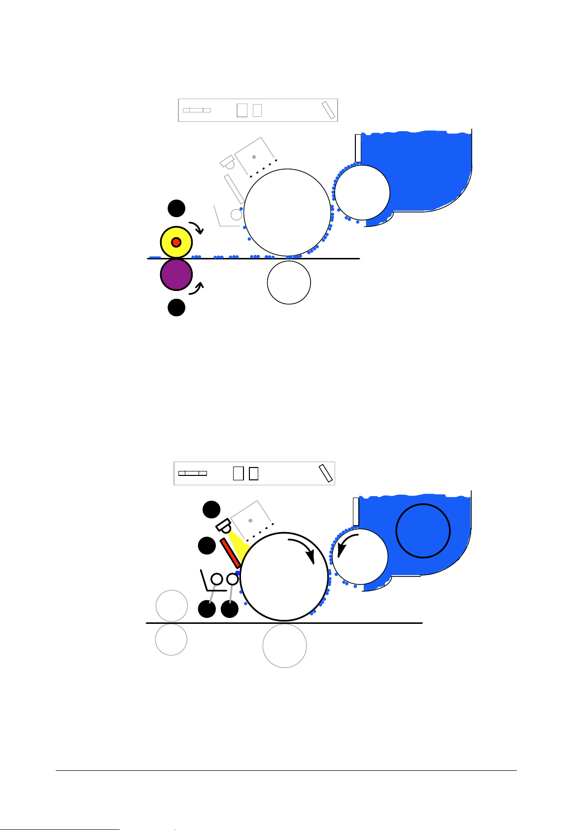
)XVLQJ
The toner on the paper is permanently fused onto the paper as it passes between the florin-finished heat roller (“A” below) and the pressure roller (“B” below) in the fuser unit. The toner is
molten and pressed into the paper. The heat roller has a halogen lamp, t urning frequ ently on and
off to maintain a preheat temperature at approxi-mately 175°C.
The heat roller temperature is constantly monitored by the engine control circuit us-ing a thermistor. For safety against overheating, the fuser system is protected by a triac which automatically opens power to the halogen lamp. If the temperature ex-ceeds 350°C, it activates the
thermo-cut device to interrupt open power to the halo-gen lamp.
0
$
2
) such as postcards, OHP, envelopes, etc., tend to require
4-10
)609<33
Page 11
2SHUDWLRQ#WKHRU\
(OHFWURSKRWRJUDSKLFV#V\VWHP
$
%
'UXP#FOHDQLQJ#DQG#HUDVLQJ#VWDWLF#FKDUJH
The drum needs to be physically cleaned of toner remaining on its surface in the pre-vious rotation. The cleaning blade (A below) is constantly pressed against the drum and scrapes the residual toner on the drum off to the refresher roller (B below). The refresher roller drives the toner to
the spiral (fins) roller (C below) at one end of which the waste toner bottle is connected to collect the waste toner.
'
$
%&
)609<33
After the drum is physically cleaned, it then must be cleaned to an electrically neu-tral state.
This is necessary to erase any residual positive charges, ready to accept th e next uniform charg e.
The residual charge is canceled by exposing the drum to the light emitted from the eraser LED
4-11
Page 12

2SHUDWLRQ#WKHRU\
(OHFWURSKRWRJUDSKLFV#V\VWHP
(D above) in the similar manner as described in page 4-6. This lowers the electrical conductivity
of the drum surface making the re-sidual charge on the drum surface escape to the ground.
7\SLFDO#SKRWR#SURFHVV#WLPLQJ#FKDUW
The following chart shows the signals used for photo processing. These signals acti-vate the corresponding device in the fol low in g t imi ng s equences. A simple description for t hes e signals follow.
)LUVW#SDJH 6HFRQG#SDJH
02725
3$3(5
0+9'5
(5$6(
%,$6
7+9'54
639'5
7DE O H#71#5## )XQFWLRQV#RI#VLJQDOV
6LJQDO )XQFWLRQ
MHVDR (Main High Voltage DRive) Drives main charger with high voltage bias. This signal is kept on during
ERASER Turns on the eraser (LED array) as soon as the motor begins revolving (A
BIAS Turns on the developer bias (on the magnet roller). The duration of this
THVDR (Transfer High Voltage
DRive)
SPVDR (SeParation Vias DRive) Turns the separation charge bias on and off. The duration of SPVDR
$
%
&
(
'
)
*
the job is processed.
above).
signal is dependent on th e current paper size (B) and turns off between
pages (C).
Turns on the transfer bias. Note that the transfer bias is reverse (+300 V)
at the beginning of a print job (D)until the paper is actua ll y fed onto the
transfer roller. This pre ve nts contamination on the back side of paper by
effectively repelling the toner during the paper is not present between the
drum and the transfer roller. The transfer bias is kept on during a print job
(E).
turned on (F) varies depending on the size of the page. SPVDR is off
between pages (G).
4-12
)609<33
Page 13

2SHUDWLRQ#WKHRU\
0
10 1
10094
MOTOR
(MAIN
MOTOR)
6
39
MHVDR
(MAIN
CHARGER)
2381 423
4
43 6
99
THVDR1
(TRANSFER
CHARGER1)
2381
THVDR2
(TRANSFER
CHARGER2)
1000 1
3362 411
FEDDR
(CASS1
FEED
CLUTCH)
1400 181
3
62
41
9
REGDR
(REGIST
CLUTCH)
181
4001
41
9 6363
LASER
VSREQ
VSREQ
1999
4092
4361 64
4
BIAS
10094
ERASER
10094
CHVON
100 8382
SCANER
2482
423
436
4844 6
99 6
2
SPVDR1
(SEPARATE
CHARGER1)
4301 6663
2482
SPVDR2
(SEPARATE
CHARGER2)
1
86 3
46 3948
908
FEEDS
(FEED
SENSER)
3819
30
6181 8092
EXITJ
(JAM
SENSER)
4411 6
3
9
831
COUNT
3ULQW#WLPLQJ#FKDUWV
715 3ULQW#WLPLQJ#FKDUWV
The following charts show timings among those signals the engine controller issues to control
printing. The charts include different timings depending on the paper sizes and paper sources.
)LJXUH#718 0DLQ#FDVVHWWH2$8#RU#$7/#+)HHG#VSHHG#>)(''5@ 5541;33#PP2V,
5
5
2 PRINT PROCESS TIMING A5/A4Y( 210 mm ) DRUM SPEED 110.000 mm/s FS-6900
7
555
7
7
5
5
7
7
7
755
7
7
7
7
7
7
5
5
5
7
5
5
77
55
5
57
221.800 mm/s 25.40 ppm 1.269 msec
)609<33
MOTOR
MHVDR
(MAIN MOTOR)
(MAIN CHARGER)
THVDR1
(TRANSFER CHARGER1)
FEDDR
THVDR2
(CASS1 FEED CLUTCH)
(TRANSFER CHARGER2)
LASER
REGDR
(REGIST CLUTCH)
4-13
BIAS
ERASER
CHVON
SPVDR1
SCANER
(SEPARATE CHARGER1)
SPVDR2
(SEPARATE CHARGER2)
EXITJ
FEEDS
(JAM SENSER)
(FEED SENSER)
COUNT
Page 14
)LJXUH#719 3)059#IHHGHU2$8#RU#$7/#+)HHG#VSHHG#>)(('4@ 5;3175#PP2V,
0
10 1
10632
MOTOR
(MAIN
MOTOR)
1093
2
MHVDR
(MAIN
CHARGER)
2919
4
281
13
THVDR1
CHARGER1)
1000
2293
23
33
46
4
1
MON1
(FEED1
MOTOR)
2901
263
23
4
1
MSL1
SPEED
CHENGE)
2901
263
1000 1600 3362 3962
CLON1
ROLLER
CLUTCH)
1930
23
4292
4
1
REGDR
(REGIST
CLUTCH)
23
4
39 4
1
6901
LASER
VSREQ VSREQ
2
3
4630
4899 6992
BIAS
10632
ERASER/CHVON
100 8920
SCANER
3020
4
4903
382
13
26
SPVDR1
CHARGER1)
4839
201
3020
SPVDR2
CHARGER2)
2160 4084 4
22 6446
FEEDS
(FEED
SENSER)
43
6268 6
19 8630
EXITJ
(JAM
SENSER)
4949
311
6493 88
COUNT
280 42 / 25 40 1 269
5
2SHUDWLRQ#WKHRU\
3ULQW#WLPLQJ#FKDUWV
55
5
2 PRINT PROCESS TIMING A5/A4Y( 210 mm ) DRUM SPEED 110.000 mm/s FS-6900
77
7
MOTOR
(MAIN MOTOR)
7
7
7
7
775 5
55
55
MHVDR
MON1
THVDR1
(MAIN CHARGER)
(TRANSFER CHARGER1)
5
5
7
7
55
MSL1
CLON1
(FEED1 MOTOR)
(FEED1 SPEED CHENGE)
(FEED1 ROLLER CLUTCH)
7
7
7
7
5
55
55
LASER
REGDR
(RESIST CLUTCH)
7
5
BIAS
ERASER/CHVON
5
7 7
7
5
775
SPVDR1
SCANER
7
5
FEEDS
SPVDR2
(SEPARATE CHARGER1)
(SEPARATE CHARGER2)
7
7
57
EXITJ
(FEED SENSER)
COUNT
(JAM SENSER)
4-14
)609<33
Page 15
2SHUDWLRQ#WKHRU\
0
10 1
111
2
MOTOR
(MAIN
MOTOR)
1613
9
MHVDR
(MAIN
CHARGER)
3439
29
801
6
THVDR1
(TRANSFER
CHARGER1)
13
0
2813
28
5
3
12
1
23
MON1
(FEED1
MOTOR)
3421
83
1000
2813
3362
1
MON2
(FEED2
MOTOR)
1000 1600 3362 3962
CLON2
(FEED2
ROLLER
CLUTCH)
24
028
4812
23
REGDR
(REGIST
CLUTCH)
28
0
9
23
421
LASER
VSREQ
VSREQ
30
1
0
419
12
BIAS
111
2
ERASER/CHVON
100 9440
SCANER
3
40
29
423
902
6
8
SPVDR1
(SEPARATE
CHARGER1)
3
9
21
3
40
SPVDR2
(SEPARATE
CHARGER2)
2680
4604
042 6966
FEEDS
(FEED
SENSER)
48
6
88
239 91
0
EXITJ
(JAM
SENSER)
469
831
013 93
COUNT
3ULQW#WLPLQJ#FKDUWV
)LJXUH#71: 6HFRQG#3)059#IHHGHU2$8#RU#$7/#+)HHG#VSHHG#>)(('5@ 5;3175#PP2V,
5
5
5
2 PRINT PROCESS TIMING A5/A4Y( 210 mm ) DRUM SPEED 110.000 mm/s FS-6900
5
75
5
7
57
77
7
55
5
7
75 5
5
7
7
5
57
75
5
7
5
75
5
75
77
5
5
5
5
75 5
57 5
5
57 77
7
5
5 5
5
5
77
5
5
5
5
7
7
7
5
77
7
280.42 mm/s 25.40 ppm 1.269 msec
)609<33
MOTOR
MHVDR
(MAIN MOTOR)
(MAIN CHARGER)
MON1
(FEED1 MOTOR)
MON2
(FEED2 MOTOR)
THVDR1
(TRANSFER CHARGER1)
CLON2
REGDR
(RESIST CLUTCH)
(FEED2 ROLLER CLUTCH)
4-15
LASER
BIAS
ERASER/CHVON
SPVDR1
SCANER
(SEPARATE CHARGER1)
SPVDR2
(SEPARATE CHARGER2)
EXITJ
FEEDS
(JAM SENSER)
(FEED SENSER)
COUNT
Page 16
)LJXUH#71; 03#WUD\2$82$7<#+)HHG#VSHHG#>03@ 5371:6;#PP2V,
0
10 1
10218
MOTOR
(MAIN
MOTOR)
6
9 6863
MHVDR
(MAIN
CHARGER)
2
0
4361 486
6
23
THVDR1
(TRANSFER
CHARGER1)
1300 18
9
3662
4241
MPFSOL
(MP
FEED
SOLENOIDO)
1000 18
9 3362 4241
MPLSOL
(MP
LIFT
SOLENOIDO)
1
24 3886
REGDR
(REGIST
CLUTCH)
1941 4303
1941
412
4303 648
LASER
VSREQ
VSREQ
2123 4216 448
6
8
BIAS
10218
ERASER
10218
CHVON
100 8
06
SCANER
68
1
2606
4361
4489
4968
6
23
68
1
SPVDR1
(SEPARATE
CHARGER1)
442
6
8
2606
SPVDR2
(SEPARATE
CHARGER2)
1
10
36
0
40
2 6032
FEEDS
(FEED
SENSER)
3943
8
4
630
8216
EXITJ
(JAM
SENSER)
4
3
689
60
9 8441
COUNT
5
2SHUDWLRQ#WKHRU\
3ULQW#WLPLQJ#FKDUWV
5
5
5
2 PRINT PROCESS TIMING A5/A4Y( 210 mm ) DRUM SPEED 110.000 mm/s FS-6900
MOTOR
(MAIN MOTOR)
7
7
5
5
7
MHVDR
THVDR1
(MAIN CHARGER)
(TRANSFER CHARGER1)
7
7
MPLSOL
MPFSOL
(MP LIFT SOLENOIDO)
(MP FEED SOLENOIDO)
7
5
5
REGDR
(RESIST CLUTCH)
57
5
LASER
BIAS
ERASER
CHVON
5
7
SPVDR1
SCANER
(SEPARATE CHARGER1)
7
7
5
SPVDR2
(SEPARATE CHARGER2)
5
5
5
7
7
7
FEEDS
(FEED SENSER)
7
7
5
5
EXITJ
(JAM SENSER)
204.738 mm/s 25.40 ppm 1.269 msec
COUNT
4-16
)609<33
Page 17

2SHUDWLRQ#WKHRU\
3DSHU#IHHGLQJ#V\VWHP
716 3DSHU#IHHGLQJ#V\VWHP
The paper feeding system picks up paper fr om the p aper cassett e or the manual feeding t ray and
at a precise timing feeds it to the electropho tography system fo r de-veloping image on the p aper.
It finally delivers the printed page to either the face-down or face-up tray.
The figure below shows the paper feeding path within the printer.
)DFH0GRZQ#RXWSXW#WUD\
0DQXDO#IHHG#
UROOHU.FOXWFK
.VHQVRU
(MHFW#UROOHUV
)XVHU#UROOHUV
5HJLVW1#UROOHUV.FOXWFK.VHQVRU
'UXP
6HSDUDWLRQ#FKDUJHU
)HHG#UROOHU.
FOXWFK.
VHQVRU
7UDQVIHU#UROOHU
3DSHU#+&DVVHWWH,
Following on the next page is another diagram showing locations of sensors, roller, and solenoids arranged along with this pape r pa th.
)609<33
4-17
Page 18
)LJXUH#71< 7UDQVSRUWDWLRQ#V\VWHP#GLDJUDP
(QJLQH#&RQWUROOHU
2SHUDWLRQ#WKHRU\
3DSHU#IHHGLQJ#V\VWHP
([LW
VHQVRU
(;,7--
([LW#UROOHUV
)DFH0GRZQ#UROOHUV
0DLQ#PRWRU
+HDW#5ROOHU
3UHVVXUH#5ROOHU
02725-
7UD QV IHU #UROOHU
3DSH U#&DVVHWWH
'UXP
5(*'5-
5HJLVW1
FOXWFK
5HJLVW#UROOHUV
5HJLVW
VHQVRU
3DSH U
VHQVRU
3$3(5-
)HHG
FOXWFK
)(''5-
0DQXDO
FOXWFK
IHHG
03)&/+-
VROHQRLG
0DQXDO
IHHG
VHQVRU
+$1'6-
0DQXDO
IHHG
03)62/-
)(('6-
&OXWFKHV 6HQVRUV 5ROOHUV
&DVVHWWH#IHHGLQJ#
The main logic controller sends the PRINT* signal to the engine controller after fin-ishing data
processing. The engine controller CPU then starts the main motor (MOTOR*), polygon motor,
registration rollers, and the fuser heater. The eng ine controller then issues the FEDDR* signal to
connect the main motor power to the paper feed tires. The tires feed the top sheet in the paper
stack in the cassette towards the registration rollers until the paper reaches the registration jam
sensor (JAMR). As the engine controller sends VSREQ to the main logic controller, the main
logic controller subse-quently issues VDO to activate the registration rollers, thus starting to
feed paper towards the drum.
The paper is advanced to the drum, to the fuser unit, triggering the exit sensor (EXITJ*), and
finally delivered either to the face-down tray or the face-up tray as switched by the ou tput stack
selector tab.
0XOWL#SXUSRVH#WUD\#IHHGLQJ
The printer recognizes the existence of paper on the multi purpose tray when the manual feed
sensor is pushed up (HANDS*).
When the print data is ready, the engine controller sends MPFSOL* to raise the lif t board by th e
solenoid. After 300 ms, the MPFCLH* signal is issued to rotate the feed roller and sends the
paper towards the registration rollers. As the registration sensor detects the paper, the lift board
lowers. The registration rollers pulls and sends the paper forwards for development.
3$35 3$7+ 1&'5
4-18
)609<33
Page 19

2SHUDWLRQ#WKHRU\
3DSHU#IHHGLQJ#V\VWHP
3DSHU#MDP#VHQVLQJ
The registration sensor and the exit (fuser) sensor keep track of the paper sent through the printerís paper path by watching the time of period during which either sensor is kept activated.
5HJLVWUDWLRQ#VHQVRU
reflector (shiny mirror surface) at the end of the actuator is in the position that can reflect the
light to shine the receptor. As the top edge of the paper reaches the registration sensor, the
reflector is pushed up and the light is interrupted(2), triggering the sensor.
Pickup of paper in the cassette is triggerred by the FEDDR* signal which drives the clutch for
the feed roller.
—A photo reflector sensor is used. While the paper is not present (1), the
➊
➋
([LW#VHQVRU
the fuser board. The actuator is in the way back at the fuser outlet. The re-flector at one end of
the actuator is normally seated in-between the photo transmitter and sensor (1). It is dressed
away out of them when the paper in the fuser sensor pushed up the actuator (2), allowing the
light to hit the receptor and turning the sensor circuit on.
—This is a photo penetration sensor, combined with an actuator arm ex-tending to
➊
➋
On detecting a paper jam, the engine controller stops printing action and shows the
message. After removing paper jam, the printer resumes printing when either the toner access
door or the feed assembly is once opened and closed. If paper jammed past the exit sensor, the
printer will not attempt to print the same page.
The printer reverts to normal operation wh en the top cover o r the paper feed unit is once o pened
and closed after removal of jam. If the paper was jammed clearing the eject sensor, the printer
does not print the same page when recovered.
Paper jam
)609<33
4-19
Page 20

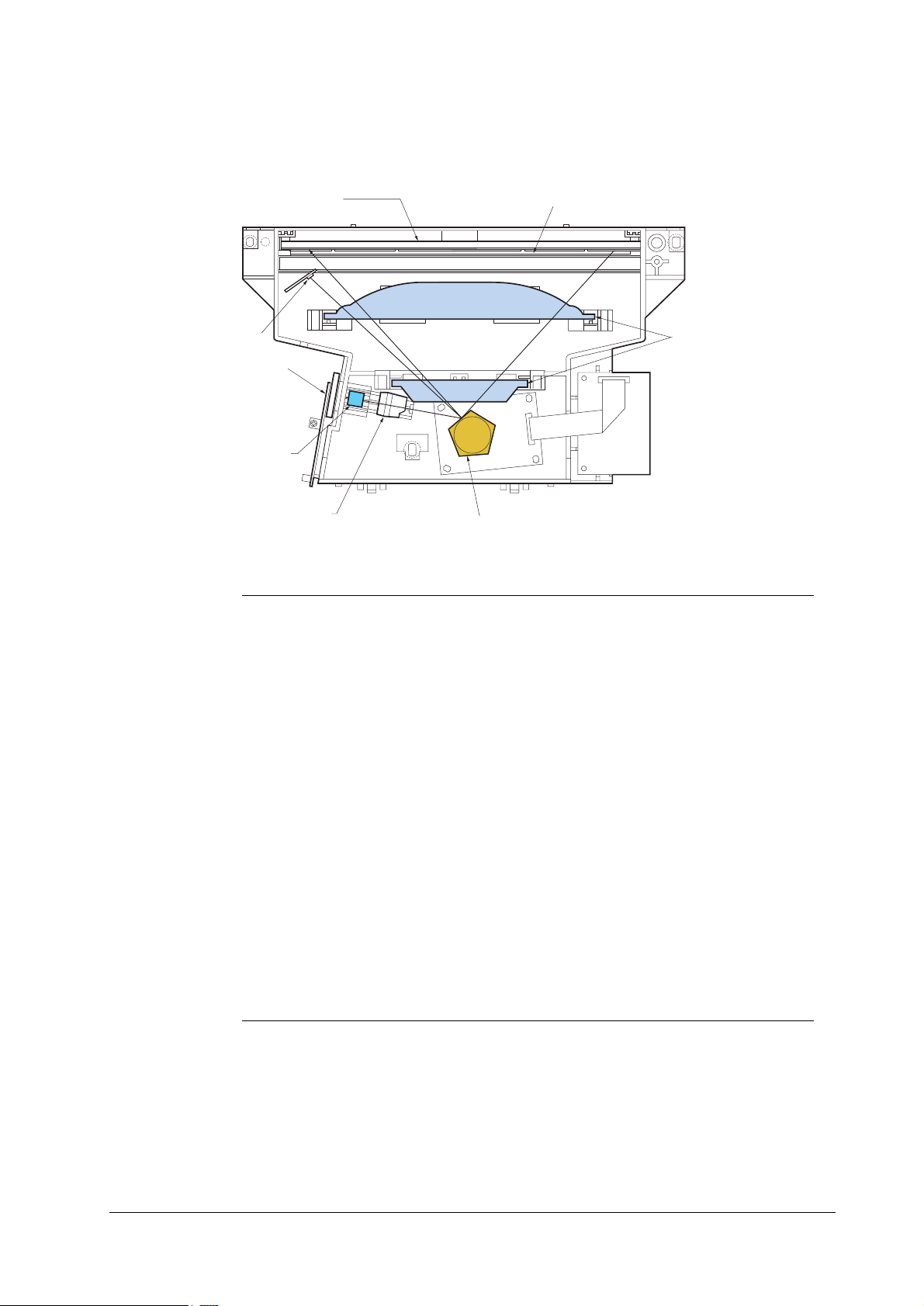
717 %DVLF#HQJLQH#IXQFWLRQV
This section presents a general functional overview of the engine system of the printer. It was
intended to provide a comprehensive knowledge on basic functions that the engine system performs during printing. The following printer functions are covered:
Engine controller system
•
Main logic controller system
•
Paper feed system
•
Power system
•
%DVLF#VHTXHQFH#RI#RSHUDWLRQ
The following figure is a simplified block diagram of the printer engine system. Details on each
segment follow.
)LJXUH#7143 (QJLQH#V\VWHP
2SHUDWLRQ#WKHRU\
%DVLF#HQJLQH#IXQFWLRQV
)DFH0XS#6WDFN
6FDQQHU#8QLW
'LRGH
3RO\JRQ#0LUURU
)XVHU#8QLW
)DFH0GRZQ#6WDFN
/DVHU
+HDW#5ROOHU
$3&
&LUFXLW
'UXP#8QLW
0DLQ#&KDUJHU
D06L#'UXP
7UDQVIHU#5ROOHU
3DSHU#)HHG#5ROOHU
0XOWLSXUSRVH
7UD\
+RVW#&RPSXWHU
,QWHUIDFH
0DLQ#/RJLF#&RQWUROOHU
/DVHU#%HDP
'HYHORSHU#8QLW
'HYHORSHU
5ROOHU
(QJLQH#&RQWUROOHU
7RQQHU
&RQWDLQHU
3DSHU#)HHG#8QLW
%*50B%$61&'5
3DSHU#&DVVHWWH
4-20
)609<33
Page 21

2SHUDWLRQ#WKHRU\
(QJLQH#FRQWUROOHU#V\VWHP
718 (QJLQH#FRQWUROOHU#V\VWHP
The engine controller provides control over all print engine activities. It drives laser, coordinates
the electrophotography process with print data from the main logic con-troller. The engine system also manages information collected back from sensors, etc., so that a message is given in
case of need for user attention.
The engine controller is responsible for the following systems, explained step by step in the following sections.
)ODVK#PHPRU\
The engine controller uses a flash memory to store environmental parameters that does not
require a battery backup. The flash memory is driven by +5 V power and de-signed to stand
reading and writing for nominally 100,000 times.
3ULQW#GHQVLW\#FRQWURO
The print density is adjusted by means of changing the clock frequency of the developer bias
system. The density is higher when the clock frequency is high; the density is lower when the
clock frequency is low.
+LJK0YROWDJH#JHQHUDWRU
Two main clocks of HVCLK1 and HVCLK2 are program-divided to g enerat e the oscillator output. This is up-verted using a transformer in the high-voltage circuit. The divisor frequency is
determined by the 8-bit register. The oscillation is toggled by the engine CPU.
/DVHU#VFDQQHU#FRQWURO
In order to activate the laser scanner, the engine controller does the following tasks:
Forced laser activation timing
•
Laser diode current limit
•
Laser power control output
•
Beam detection photo-sensor output
•
Polygon motor activation
•
Polygon motor readiness detection
•
3RO\JRQ#PRWRU#FRQWURO
The output frequency signal to the polygon motor is generated by the engine gate ar-ray as it
divides the engine system clock (16 MHz). The polygon motor is of 26,596 rpm and the frequency is 2659.57 Hz.
)609<33
As the laser beam reaches the beam detector sensor, the sensor board generates the horizontal
synchro signal (PD*). This signal makes the engine gate array consequently turn the video output signal (VDO*) and the APC signal (LONB*) high which respectively activate the laser light
and the APC controller.
The engine CPU attempts to detect the horizontal synchronization signal so that the laser diode
is normally trigger ed. If the horizo ntal sync hronizatio n output is not found af ter the laser dr iving
4-21
Page 22
current control (LENB*) is set low, the engine CPU recognizes it as the failure on the APC
board and gives the E3 error.
6DIHW\#LQWHUORFN
For safety purpose, micro switches are provid ed to sense that either the top (t oner access) or sid e
(drum access) cover is open. These switches, when the applicable cover is open, open and disconnect the DC power to the laser scanner as follows.
The laser emission is deactivated when either cover is open in the following system.
The interlock power su pply of +5 V i s g enerated by downv erting the +2 4 V DC power u sing the
3-terminal regulator. The +5 V DC is used as the power supply for the scanner APC circuit that
is cut out when either cover is open. At the same time as the cover is open, the control signal
output for the scanner unit, that is derived from the engine gate array, is set to the high-impedance state.
)LJXUH#7144 ,QWHUORFN#V\VWHP
2SHUDWLRQ#WKHRU\
(QJLQH#FRQWUROOHU#V\VWHP
7RS #FRYHU#VZLWFK
/HIW#FRYHU#VZLWFK
.579'&
(QJLQH
J2D
9
7RS #FRYHU#VZLWFK
/HIW#FRYHU#VZLWFK
.579'&
60WHUP1
UHJXODW1
.89'&
3RO\JRQ#PRW1
$3&
4-22
)609<33
Page 23

2SHUDWLRQ#WKHRU\
(QJLQH#FRQWUROOHU#V\VWHP
7KH#HQJLQH#JDWH#DUUD\
The engine gate array is a supplementary device to the Engine CPU. The gate array is a CMOS
type, 4100-gate, 100-pin QFP that has the following internal blocks.
Address decoder
•
Registers
•
Interrupt handler
•
Ports A to F
•
Data selector
•
Overrun detector
•
Port mode controller
•
Kyocera I/O controller
•
Print density controller
•
Laser power controller
•
Decoder g/a flash
•
High-voltage clock genera tor
•
Test-print controller
•
Engine CPU address-hold controller
•
Interlock controller
•
3LQ#DVVLJQPHQW
Pin assignment for the engine gate array is ta ble on the followin g pages. The dev ice in Remarks
column means those which the signal is forwarded to.
7DE O H#71#6## J2D#SLQ#DVVLJQPHQW³426
3LQ#QR1 6LJQDO J2D#VLJQDO ,Q22XW )XQFWLRQ /RJLF 5HPDUNV
1 THVDR1* THVDR OUT Transfer charger voltage 1 Neg. HV board
2 CHVON* REVBN OUT Transfer bias control output, L: On Neg. HV board
3 VDD VDD Power terminal (+5 V)
4 VSS VSS Power terminal (Ground)
5 MHVDR* MHVDR OUT Main charger control output, L: On Neg. HV board
6 B IAS* BIAS OUT Bias DC volt age control output, L: 100 V , H:
100 V
7 E RASE* ERAS EN OUT Eraser control output, L: O n Neg. Eraser
8 FDNSD* PC3 OUT Face-down solenoid control output, L: On Neg. FU/D solenoid
9 FAN * PC2 OUT Fan motor c ont rol out put , L: On Pos. Fan (Body, C-
10 EXITJ* PA1 IN Fuser sensor input, H: No paper Neg. Fuser
11 WTONR* PA0 IN Wast e toner bottle full detection, L: ful l Neg. 12 OPSEL2 PB5 OUT Option uni t selec t code 2 Neg. Option unit
13 THVDR2* PD4 OUT Transfer charger voltage control output 2 Neg. HV board
14 FEEDS* PA2 IN Registration sensor input, L: No paper - 15 VSS VSS Power terminal (Ground)
16 PAPER* PA4 IN Cassette paper detection, L: Empty
Neg. HV board
box)
)609<33
4-23
Page 24

2SHUDWLRQ#WKHRU\
(QJLQH#FRQWUROOHU#V\VWHP
7DE O H#71#6## J2D#SLQ#DVVLJQPHQW³526
3LQ#QR1 6LJQDO J2D#VLJQDO ,Q22XW )XQFWLRQ /RJLF 5HPDUNV
17 HANDS* PA3 IN Multi paper feed slot paper detection, L: Paper Neg. MP unit
18 TNCON* PB1 I N Waste toner reservoir dete c ti on, L: Insta lled Neg. 19 OPSEL1 PB4 OUT Option unit select code 1 Neg. O ption unit
20 OPSEL0 PB3 OUT Option unit select code 0 Neg. O ption unit
21 RDY* PB2 OUT Print ready output, L: Ready - 22 PHEAT PC5 OUT Not used Pos. 23 FUPSD* PC4 OUT Face-up solen oid contro l output, L: On Neg. FU/D solenoid
24 SPVDR1* PD1 OUT Reve rse bi a s control out put , L: On Neg. HV board
25 SPVDR2* PD0 OUT Re ve rse bi as current control output Neg. HV board
26 TEST1 TEST1 IN G/A test input 1, H: Test mode Jumper
27 TEST0 TESTN IN G/A test mode, L: Test mode Fixed high
28 VDD VDD Power terminal (+5 V)
29 VSS VSS Power terminal (Ground)
30 TESTCLK TSTCLK IN G/A test clock Fixed low
31 ILOCK PB0 IN Interlock input, L: Interlock on Pos. 32 ERRDY* PA5 I N Eraser blow-out det., L: Blown E ra ser
33 THSBY PD5 OUT Fuser heater control, L: Print; H: Idle Fuser
34 FRMCE* FCS* OUT Flash ROM chip select Neg. Flash ROM
35 MPFSOL* PC1 OUT Multi paper feed solenoid control, L: On Neg. MP unit
36 FEDDR* PC0 OUT Paper pickup roller clutch control, L: On Neg. Clutch
37 REGDR* PD7 OUT Regist. roller clutch control, L: Off Pos. Clutch
38 SCCLK SCCLK OUT Polygon motor clock Pos. Scanner
39 PDIN PDIN IN Beam de te c t Neg. Scanner
40 VSS VSS Power terminal (Ground)
41 NON LATCH OUT Not used Pos. 42 NON DSCLK OUT Not used Pos. 43 NON SDATA OUT Not used Pos. 44 VDOUT VDOUT OUT Video data Neg. Scanner
45 LASER PC7 OUT Laser diode drive control Pos. Scanner
46 LONB* LONB OUT APC control, L: Sampling Neg. Scanner
47 SCANR* PC6 OUT Polygon motor contro l, L: O n Neg. Sc anner
48 SCRDY* PA7 IN Polygon motor ready, L: Ready Neg. Scanner
49 MOTOR* PD3 OUT M a in mot or c ontrol, L: On Neg. Main motor
50 EGIR* PF0 OUT System error interrupt, L: interrupted Pos. 51 X1 CKO0 OUT Clock (Engine CPU)
52 X2 CKO1 OUT Clock (Engine CPU)
53 VDD VDD Power terminal (+5 V)
54 VSS VSS Power terminal (Ground terminal)
55 CLCK* CLCKN IN G/A test clock clear, L: Clearing Fixed high
56 XTO XTO IN Oscillator (16.9344 [MHz])
57 XTI XTI IN Oscillator (16.9344 [MHz])
58 GAINT INTO OUT Engine error interrupt, H: interrupted Pos. 59 RESET* RST N IN Power on re set Neg.
60 ASTB ASTB IN Engine CPU ASTB
61 WR* WRN IN Engine CPU WR* Neg.
62 RD* RDN IN Engine CPURD* Neg.
4-24
)609<33
Page 25

2SHUDWLRQ#WKHRU\
(QJLQH#FRQWUROOHU#V\VWHP
7DE O H#71#6## J2D#SLQ#DVVLJQPHQW³626
3LQ#QR1 6LJQDO J2D#VLJQDO ,Q22XW )XQFWLRQ /RJLF 5HPDUNV
63 A16 A 16 IN Engine CPU address
64 A15 EA15 IN Engine CPU address
65 VSS VSS Power terminal (Ground)
66 A14 EA14 IN Engine CPU address
67 A13 EA13 IN Engine CPU address
68 A12 EA12 IN Engine CPU address
69 AD7 AD7 IN/OUT Engine CPU address/data bus
70 AD6 AD6 IN/OUT Engine CPU address/data bus
71 AD5 AD5 IN/OUT Engine CPU address/data bus
72 AD4 AD4 IN/OUT Engine CPU address/data bus
73 AD3 AD3 IN/OUT Engine CPU address/data bus
74 AD2 AD2 IN/OUT Engine CPU address/data bus
75 AD1 AD1 IN/OUT Engine CPU address/data bus
76 AD0 AD0 IN/OUT Engine CPU address/data bus
77 EA7 EA7 OUT Engine CPU address ROM address
78 VDD VDD Power terminal (+5 V)
79 VSS VSS Power terminal (Ground)
80 EA6 EA6 OUT Engine CPU address ROM address
81 EA5 EA5 OUT Engine CPU address ROM address
82 EA4 EA4 OUT Engine CPU address ROM address
83 EA3 EA3 OUT Engine CPU address ROM address
84 EA2 EA2 OUT Engine CPU address ROM address
85 EA1 EA1 OUT Engine CPU address ROM address
86 EA0 EA0 OUT Engine CPU address ROM address
87 MPLSOL* PD2 IN Multi paper feed clutch control, L: On Neg. MP unit
88 HEATT PD6 OUT Fuser heater control, H: On Fuser
89 VIDEO VDOIN IN Video data Neg. Scanner
90 VSS VSS Power terminal (Ground)
91 PDOUT* PDOUT* OUT Beam detect sensing Neg. Main log. board
92 S/C SC IN/OUT Main I/F status command M ain I/F
93 SCLK SCLK IN Main I/F status command clock Main I/F
94 CBSY* CBSYN IN Main commands in transmission Neg. Main I/F
95 SBSY* SBSYN OUT Engine status in transmission Neg. Main I/F
96 CINH* CINHN OUT Engine busy Neg. Main I/F
97 HVCLK1 HVCK1 OUT HV unit clock 1 HV board
98 HVCLK2 HVCK2 OUT HV unit clock 2 HV board
99 TONER PA6 IN Remaining toner sensing , L: Empty HV board
100 PSEL HVOL OUT Transfer bias (Thick/normal paper) HV board
)609<33
4-25
Page 26

2SHUDWLRQ#WKHRU\
(QJLQH#FRQWUROOHU#V\VWHP
3RZHU#VXSSO\
The power supply contains the AC and DC power and distribution circuitry on the board. The
high voltage generator is not included on this board but on the separate high-voltage board.
The power supply circuit is diagrammed on page 4-27, Figure 4.12.
$&#LQSXW#DQG#UHFWLILHU
line filter circuit (L4, L5, C3, etc.) and rectified by diode array BD1 to DC power. Transistor Q1
performs switching of the DC power output for downverting it to the 24 V and 5 V AC voltage
by means of transformer T1.
57#9#'&#SRZHU#OLQH
C18 and delivered to connectors CN5 for distribution. The 24 V DC power is referred to as
VDD or VDDCOM and is used by the following components in the en-gine system:
Face-up/down stack solenoids
•
Clutches (registration, feed, manual-feed)
•
Eraser
•
Fans
•
High-voltage generator (board)
•
Main motor and laser polygon motor
•
Clutches, motors, solenoids within the option units
•
The 24 V DC power is forcibly interrupted for safety whenever the printer top cover or the drum
unit access door is opened. For details, see page 4-22,
8#9#'&#SRZHU#OLQH
etc., like as for the 24 V DC power line. It also delivered to CN3 and CN4. The 5 V DC power
is referred to as VCC and is comprehensivel y used by t he mai n control-ler, sensors, engine controller, etc.
—Either 120 V or 230 V AC power arriving at CN1 is fed to the AC
—The 24 V AC at the secondary output of T1 is rectified by D1 and C13/
6DIHW\#LQWHUORFN
—The 5 V AC at the secondary output of T1 is rectified by D2 and C14/1 5,
.
3RZHU#SURWHFWLRQ#FLUFWXLW
tection circuit is provided to avoid damaging the circui t.
)XVHU#KHDWHU#SRZHU#FRQWURO
across CN2. The heater is switched on and off as being controlled by TRIAC TRC1. TR C1 turns
on the heater when HEATCOM (pin 8) at CN3 is energized by command from the engine controller.
—In case of short-circuiting in the 5 V or 24 V DC load side , a pro-
—On the AC primary side, the fuser heater is wired in series
4-26
)609<33
Page 27

2SHUDWLRQ#WKHRU\
(QJLQH#FRQWUROOHU#V\VWHP
)LJXUH#7145 3RZHU#VXSSO\#FLUFXLW#GLDJUDP
)609<33
4-27
Page 28

719 /RJLF#FRQWUROOHU#V\VWHP
The logic controller system does the following:
Communicates with the host computer to receive data at one of the printer’s in-terface
•
Analyzes and translates the print data to be the dot data in the raster memory
•
Communicates with the engine system to discern radiness for printing
•
Stores fonts and macro information
•
The main logic controller has specifications as shown in the following section. A simplified diagram is shown on page 4-29, Figure 4.13.
7DE O H#71#7## 0DLQ#FRQWUROOHU#VSHFLILFDWLRQV
,WHP 6SHFLILFDWLRQ
CPU PowerPC603e-100MHz
System ROM size 4 MB (16 Mbit × 2)
RAM size Standard 16 MB SIMM
Max. 64 MB (2 PC SIMM slots)
Fonts Resident 4 MB (32 Mbit × 1)
Socket 2 MB [PK-5 (Option)]
API ROM 512 kB
Memory card 1 slot/JEIDA 4.2 or PCMCIA 2.0
Interface Parallel High-speed bi - directional [IEEE 12 8 4]
Serial RS-232C/RS-422A
Option 2 slots
Engine communic at ion mode Serial interface
Front panel com . m ode Serial interface
Others Sm oothing KIR (Vector compensation)
Toner savor EcoPrint [On/Off]
Reduction Main and sub scan
Video clock 26.2186 MHz
2SHUDWLRQ#WKHRU\
/RJLF#FRQWUROOHU#V\VWHP
4-28
)609<33
Page 29

2SHUDWLRQ#WKHRU\
/RJLF#FRQWUROOHU#V\VWHP
)LJXUH#7146 0DLQ#FRQWUROOHU#EORFN#GLDJUDP
1998.12.25
YC1
IOA2-16,21
Option I/F
(OPT2/HDD)
Option I/F
(OPT1)
YC2
IOA2-16,21
LD0-15
OP1CSN CTLRDY1 OP1DACKN LIORN1 LIOWN1
OP1ACKN OP1IRN OP1DREQ
LD0-15
FLASH ROM/MASK ROM
(1M*16)*2
DIMM
Code
ROM
YS1
LDO
LS373x3
OP2CSN CTLRDY2 OP2DACKN LIORN2 LIOWN2
OP2ACKN OP2IRN OP2DREQ
U4-6
IOA5-22
IOA2-24
A2-24
Address
D0-31
Data
LD0-15
EDEVALTN
ABBN
YC3
U7 U8J U9E
(FONT:4MB, Option:2MB, API:512K)
MASK ROM/EPROM
BICA1
LS367x4
U12-15
X1
X’tal(Video)
IOCA1
IOA2-24 BICA2-24
IOA2-21
LD0-15
FA0
D32CSN00-01,D32OEN0,D32WEN0
D32A02-04
FONTOEN1-3
DPPBCLK(33.33MHz)
CARD
LS245x2
U16,17
X2
TBM(System)
26.2186MHz
DD0-31
DRAM
U10-11
BICD0-15
LD0-15
OE
(1M*16)*2
CARDDET1,2
YC6
CPRDY PRINTN VSYNCN VDATA
RDYN OUTPEN VSREQN PDOUTN
CARDCEHN CARDCELN CARDOEN CARDWEN
CARDREGN CARDRSTN
CARDRDY CARDWP BVD1,2
66.6667MHz
YS2
SIMM
SLOT2
RESETN
OE
YS3
4,8,16,32MB
Engine I/F
FPDIR FPCLK
FPDATA
SC
ESIGIR SBSYN CINHN
CBSYN SCLK
OE
16MB
SIMM
SLOT1
(4,8,16,32MB)
RESETN
U25
HCT08
3.3V
REGULATOR
U24
3.3V
CPUBCLK(33.33MHz)
RESETN
CPUABBN
A0-29D0-31
TT1 TT3 TSIZ0-2 TBSTN DBBN
AACKN TAN TEAN
CARDDET1,2
APPBCLK(33.33MHz)
A0-29
CPU
U1
PPC603e-100MHz
AACKN
TAN
TEAN
INTN
LD0-15 D0-31 A20-29
LV161284
U18,21
ACT1284
FS-6900 Controller Block Diagram
Parallel I/F
BUSY ACK PERROR
FAULT SELECT etc
STB SELECTI
INIT AUTOFD etc
YC4
CPULBGN CYCCODE0-2 DMAREADN
DPPTAN LOADN BNDEWN
APP+ DPP+
U2 U3
CEND0-7
U20 HC221
Data1-8
MBCG46533 uPD82280
RSSEL
456
CDIR COEN
MRASN0
CAS
DRWEN0
U22
Serial I/F
TXD RTS DTR
YC5
MRA0-10
MC145407
RXD
CTS DSR
8
7
123
ORASUN3
ORASLN3
9
RDA
U23
MAX488
RDB
SDA SDB
ORASUN4
ORASLN4
RESETN
ORA0-10
DRWEN1
LDO
DBTXD
DBRXD
DBCLK
Debugger
YC7
OUTPEN VSREQN
:No mounted
)609<33
4-29
Page 30

2SHUDWLRQ#WKHRU\
/RJLF#FRQWUROOHU#V\VWHP
3ULQWLQJ#GDWD#SURFHVVLQJ
The printer communicates with the host computer for receiving the print data at one of the
printer’s interfaces and temporarily store them in the interface buf fer. The main logic controller
analyzes the data for translating them into the dot data ac-cording to the original print image.
The resultant dot data are depicted in the raster memory (DRAM’s).
While data processing is in course, on the other hand, the main logic controller CPU talks to the
engine CPU via the engine interface, to discern the readiness of the printer’s engine for printing.
If the engine is ready to start printing, the main controller issues print signal to-wards the engine
controller which request the paper feed. In synchronization with the procerssion of the paper
within the printer, video data in the raster memory is released. Thus the video data are transfered
to the laser scanner together with the horizontal synchronization signal and the video clock.
On reception of the video data, the laser diode turns on and off to constitutes the print image
over the drum. The image on the drum, referred to as the static latent image, is applied with
toner, transferred onto the paper, and finally fused perma-nently on the paper by means of heat
and pressure.
6\VWHP#520
The system DIMM (YS1) accommodates system codes. The DIMM mounts two flash ROMs.
For firmware upgrade, the system DIMM is detachable for easy replacement.
7DE O H#71#8## 6\VWHP#520
Socket No. YS1
Pins 72 (DIMM)
Size 4 Mbyte
Composition 16 Mbit × 2
Access speed <100 ns
0DLQ#5$0
The RAM temporarily stores print data and font information transferred from the host buffers.
The standard RAM size is 4 MB. The size of the RAM is expandable using comprehensive PC
SIMMs.
7DE O H#71#9## 0DLQ#5$0
Number of RAMs 2
Socket Nos. U10, U11
Number of pins 42, SOJ
Size 4 MB
Composition 2 MB (1 MB × 16 bits × 2)
Access speed <80 ns
4-30
)609<33
Page 31

2SHUDWLRQ#WKHRU\
/RJLF#FRQWUROOHU#V\VWHP
The expansion SIMM should incorporate the following features:
7DE O H#71#:## ([SDQVLRQ#6,00
Number of SIMM sockets
Socket Nos. YS2
Number of pins 72
Size 4/8/16/32 MB
Access speed <80 ns
1
0HPRU\#FDUG#VORW#LQWHUIDFH
The controller accepts a SRAM or flash type memory card that comforms to the PCMCIA (version 2.1) or JEIDA 4.2 standards.
2SWLRQ#LQWHUIDFH
The printer has two open slots for installing an optional interface card (such as a se-rial interface
card or an Ethernet network interface card) and/or a harddisk drive. This interface utilizes DMA
data transfer for optimum performance.
&DXWLRQ 7KH#KDUGGLVN#GULYH#PXVW#EH#LQVWDOOHG#LQWR#WKH#OHIW0KDQG#VLGH#VORW#
+ZKLFK#LV#FORVHU#WR#WKH#SDUDOOHO#LQWHUIDFH,1#
The option interface has the following features:
7DE O H#71#;## 2SWLRQ#LQWHUIDFH
Card connector 60
Applicable interface card SEH EcoLAN 2000E
Applicable harddisk
drive
Kyocera HD-2 (2 GB)
The following table shows pin assignments for the option slots.
7DE O H#71#<## 2SWLRQ#LQWHUIDFH#SLQ#DVVLJQPHQW³426
3LQ#1R1 6LJQDO 'LUHFWLRQ 'HVFULSWLRQ
1 (A1) +5 V — —
2 (B1) +5 V — —
3 (A2) +5 V — —
4 (B2) NC — Reserved
5 (A3) GND — —
6 (B3) NC — Reserved
7 (A4) NC — Reserved
8 (B4) A15 In System address 15
9 (A5) GND — —
10 (B5) A14 In System address 14
11 (A6) A13 In System address 13
12 (B6) A12 In System address 12
13 (A7) A11 In System address 11
)609<33
4-31
Page 32

7DE O H#71#<## 2SWLRQ#LQWHUIDFH#SLQ#DVVLJQPHQW³526
3LQ#1R1 6LJQDO 'LUHFWLRQ 'HVFULSWLRQ
14 (B7) A10 In System address 10
15 (A8) A9 In System address 9
16 (B8) A8 In System address 8
17 (A9) GND — —
18 (B9) A7 In System address 7
19 (A10) A6 In System address 6
20 (B10) A5 In System address 5
21 (A11) A4 In System address 4
22 (B11) A3 In System address 3
23 (A12) A2 In System address 2
24 (B12) A1 In System address 1
25 (A13) GND — —
26 (B13) NC — Reserved
27 (A14) OP2IF* In Option interface select (L)
28 (B14) OP2ACK* Out Data acknowledge (L)
29 (A15) OP2IR* Out Interrupt Request (l)
30 (B15) NC — —
31 (A16) RDY In Kyocera Board Ready
32 (B16) DREQ Out DMA Request
33 (A17) GND 34 (B17) DMACK* In DMA Acknowledge (L)
35 (A18) IOR* In I/O Read Strobe (L)
36 (B18) IOW* In I/O Write Strobe (L)
37 (A19) R E S E T* In Reset (L)
38 (B19) NC 39 (A20) D15 In/Out System Data 15
40 (B20) D14 In/Out System Data 14
41 (A21) GND 42 (B21) D13 In/Out System Data 13
43 (A22) D12 In/Out System Data 12
44 (B22) D11 In/Out System Data 11
45 (A23) D10 In/Out System Data 10
46 (B23) D9 In/Out System Data 9
47 (A24) D8 In/Out System Data 8
48 (B24) D7 In/Out System Data 7
49 (A25) GND 50 (B25) D6 In/Out System Data 6
51 (A26) D5 In/Out System Data 5
52 (B26) D4 In/Out System Data 4
53 (A27) D3 In/Out System Data 3
54 (B27) D2 In/Out System Data 2
55 (A28) D1 In/Out System Data 1
56 (B28) D0 In/Out System Data 0
57 (A29) GND 58 (B29) +5 V -
2SHUDWLRQ#WKHRU\
/RJLF#FRQWUROOHU#V\VWHP
4-32
)609<33
Page 33

2SHUDWLRQ#WKHRU\
/RJLF#FRQWUROOHU#V\VWHP
7DE O H#71#<## 2SWLRQ#LQWHUIDFH#SLQ#DVVLJQPHQW³626
3LQ#1R1 6LJQDO 'LUHFWLRQ 'HVFULSWLRQ
59 (A30) +5 V 60 (B30) +5 V -
3DUDOOHO#LQWHUIDFH
The parallel interface supports the protocols defined by the IEEE 1284 standards. To gain conformity to these standards, the printer supports the ECP an d nibble modes.
Details on the signals on the parallel interface are described in the appropriate ap-pendix in this
manual.
6HULDO#LQWHUIDFH
The printer incorporates a port for the seri al interface. The serial interface controller is included
within the gate array and supports both the RS-232C and RS-422A protocols. Since the RS232C support is designed to be compatible with SNMP (Simple Network Management Protocol), CTS and DSR signals are included. Switching to either mode is toggled by changing a
jumper wire arrangement on the controller board. A 25-pin D-sub connector is used for the
serial port. The RS-422A extra signal lines are assigned to some of the vacant RS-232C terminals. (See Appendix A for the interface later in this manual for details.)
The serial interface has the following features:
7DE O H#71#43##6HULDO#LQWHUIDFH
Connector type 25-p in, D-sub
Baud rates/sec. 300/600/1200/2400/4800/9600/19200/38400/57600/115200
Modes RS-232C/RS-422A (switchable)
(QJLQH#LQWHUIDFH
The interface to the engine system is based on the serial interface, not the parallel in-terface that
was used with the previous line-up of the Ecosys printers. The serial-to-parallel conversion is
executed on a hardware basis.
The engine board is detachable from the printer at its interface connector. The engine interface
connector has the following pin assisngments:
Engine interface connector assignment is as follows (“*” means negative-logic.):
7DE O H#71#44##(QJLQH#LQWHUIDFH#FRQQHFWRU#DVVLJQPHQW³425
3LQ#1R1 7HUPL Q DO 6LJQDO 3LQ#1R1 7H U P L Q D O 6LJQDO
A1 GND GND B1 GND GND
A2 VCC VC C B2 VCC VCC
A3 VCC VC C B3 VCC VCC
A4 RPORT EGIR* B4 D/CZ NC (Reserved)
A5 VSREQZ VSREQ* B5 SBSYZ SBSY*
A6 CBSYZ CBSY* B6 SCLK SCLK
A7 S/CZ SC B7 CPRDY CPRDY
A8 RDYZ RDY* B8 CINHZ CINH*
)609<33
4-33
Page 34

7DE O H#71#44##(QJLQH#LQWHUIDFH#FRQQHFWRU#DVVLJQPHQW³525
3LQ#1R1 7HUPL Q DO 6LJQDO 3LQ#1R1 7HUP LQ D O 6LJQDO
A9 RXD NC (Reserved) B9 VCC VCC
A10 TXD NC (Reserved) B10 FRM/BYZ NC (Reserved)
A11 FPDATA FPDAT B11 VSYNCZ VSYNC*
A12 PRINTZ PRINT* B12 PDZ PDOUT*
A13 RESETZ RST* B13 FPSCLK FPCK
A14 LEN OUTPE* B14 VDO VIDEO
A15 GND GND B15 FPDRC FPDR
A16 GND GND B16 GND GND
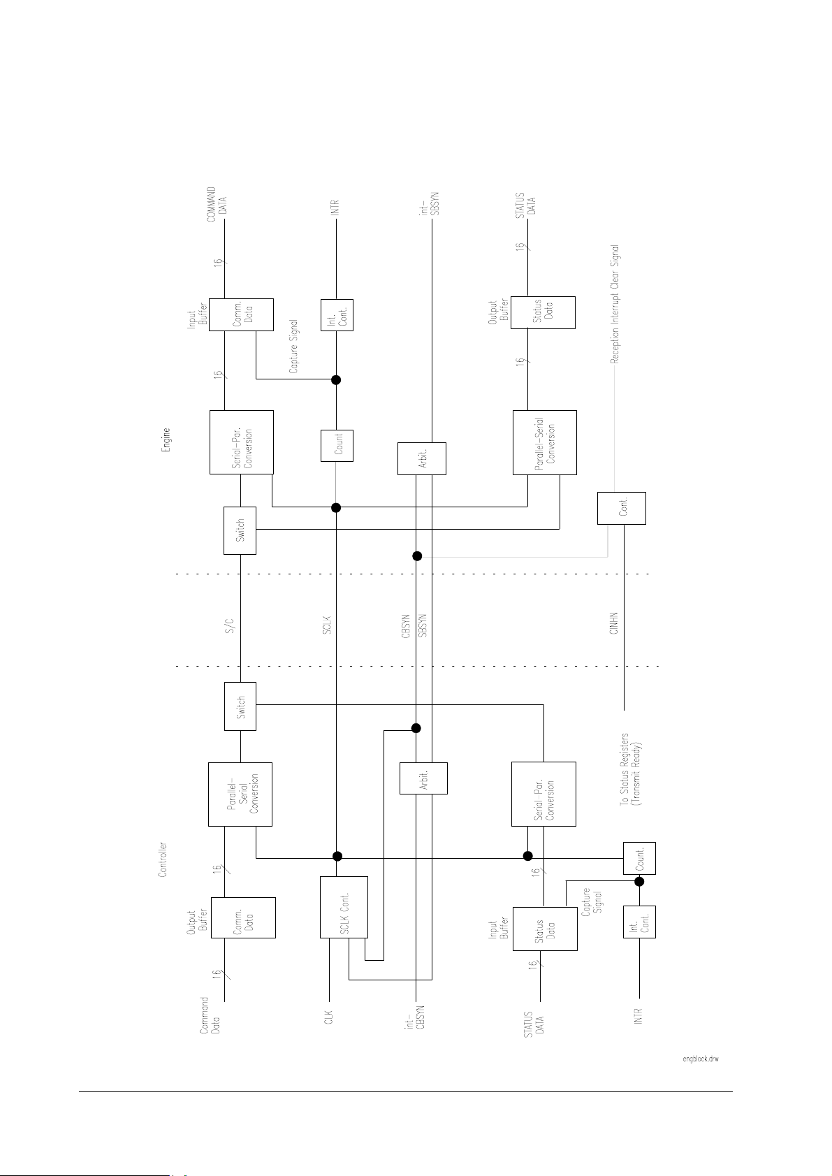
6LJQDOV#XVHG#IRU#WKH#HQJLQH#LQWHUIDFH
The following signals are used for the engine interface communication. Figure on next page
shows a simplified function diagram of the engine interface and the signals.
2SHUDWLRQ#WKHRU\
/RJLF#FRQWUROOHU#V\VWHP
7DE O H#71#45##(QJLQH#LQWHUIDFH#VLJQDOV
6LJQDO 0HDQLQJ $FWLYH 'HILQLWLRQ
SBSYN Status-BuSY-
sigNal
CBSYN Command-
BuSY-sigNal
S/C Status-data/
Command-data
SCLK Serial CLocK - Th e wi dth of the clock pulse is approx. 1µsec (960 ns). SCLK
CINHN Command IN-
Hibit sigNal
Low Determines which direction for the engine system to tra nsfer
the status data. If SBSYN is true, the controller is unable to
transfer the co mmand da ta to ward s th e engi ne s yste m. Th e con troller can read in the status data transferred from the engine
system by forwading SCLK to the engine.
Low Determines which direction for the controller system to transfer
the command data. If CBSYN is true, the co ntrolle r can transfer
the command data towards the en gine system by forwading
SCLK to the engine system
- This is a bi-directional seria l da tum containing the stat us da ta
and command data as well as attributive information. The transfer data commences wit h LSB, then to MSB.
is the clock delivered by the controller and used to synchro-nize
the status data and command data with each other.
Low This signal inhibits the signal transmission. If CINHN is low,
the controller is not allowed to ready the transmission data.
This inhibit is cancelled when the engine controller reads in the
reception data.
4-34
)609<33
Page 35
2SHUDWLRQ#WKHRU\
/RJLF#FRQWUROOHU#V\VWHP
(QJLQH#LQWHUIDFH#EORFN#GLDJUDP
)609<33
4-35
Page 36

This page left blank intentionally
2SHUDWLRQ#WKHRU\
/RJLF#FRQWUROOHU#V\VWHP
4-36
)609<33
 Loading...