

Page 1

MITAC Desktop Board PH10LU
Product Guide
Page 2

2
Desktop Board Features
This chapter briefly describes the features of Desktop Board PH10LU.
Table 1 summarizes the major features of the Desktop Board.
Feature Summary
T
AB LE
1 . MITAC D
ES K TOP BOA R D
PH10LU F
EA T URE S
Form Factor Micro-ATX (244 millimeters [9.6 inches] x 244 millimeters [9.6
inches])
Processor 4rd generation Intel® Core processor family with up to 95 W
TDP in an LGA1150 socket
Main Memory
Support for DDR3 1066/1333/1600 MHz SO-DIMMs
(DDR3 1333 MHz and DDR3 1600 MHz SO-DIMMs operate
at 1066 MHz only)
Support for up to 32 GB of system memory
240-pin DDR3 DIMM
4
Chipset Intel® Q87 Platform Controller Hub (PCH)
Integrated
Graphics
Intel® Graphics Media Accelerator 4600 (Intel® GMA 4600)
External Graphics
External graphics support provided through the PCIe 3.0 x16
bus connector
Audio
RealTek* ALC662/888 audio codec for 5.1 (6-channel) High
Definition Audio (HD Audio) and AC ’97 Audio.
Front panel microphone/headphone header with support for HD
Audio or AC ’97 Audio
Legacy I/O
Legacy I/O Controller (Nuvoton* NCT6104D) that provides:
Hardware management support
Serial Port (Rear IO) 2
Serial Port (On board) 2
Parallel port via an onboard header 1
Expansion
Capabilities
PCIe 3.0 x16 (Blue) 1
PCIe 2.0 x1 (Black) Either Option
PCIe 2.0 x1 (Black) 1
PCIe 2.0 x16 (x4 Lanes)
1
Page 3

3
PCI Express* Full-Mini Card slot with Half-Mini
Card support
Either Option
Peripheral
Interfaces
USB 3.0 back panel connectors (blue)
2
USB 2.0 back panel connectors (black)
4
USB 3.0 front panel ports
2 (Headers)
USB 2.0 front panel ports
4 (Headers)
Serial ATA (SATA) 6.0 Gb/s interfaces
6
Hardware Monitor
Subsystem
Hardware monitoring through the Nuvoton* NCT6104D legacy
I/O controller, including:
Remote thermal sensor
4-pin system fan header
LAN Support
Intel® I217 Gigabit (10/100/1000 Mb/s) LAN
Intel® I210 Gigabit (10/100/1000 Mb/s) LAN
BIOS
AMI UEFI BIOS Support for Advanced Configuration and Power
Interface (ACPI)
Instantly Available
PC Technology
Support for PCI Express Revision 3.0
Wake on USB, PCI Express, LAN, serial, PS/2, and front
panel
Power Requirement ATX12V
Environment
Operating Temperature: 0 °C to +50 °C
Storage Temperature: -20°C to +70°C
Safety
CE
FCC
UL
Page 4
4
Desktop Board Components
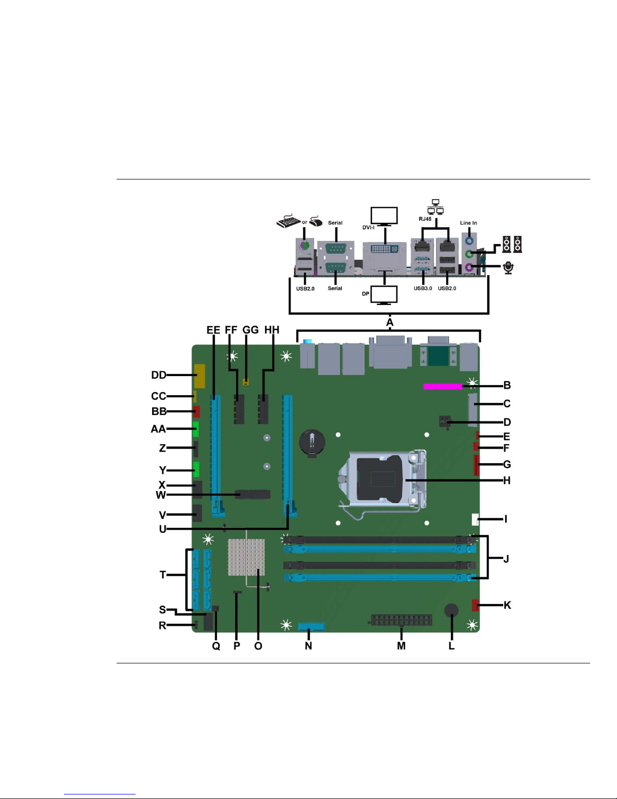
Figure 1 shows the approximate location of the major components on the top side of
MiTAC Desktop Board PH10LU.
Fi g u re 1. Mi TA C Desktop Bo a r d P H 10LU Compon e n t s (Top)
Page 5

5
T
AB L E
2 . MITA C D
ES K TOP BOA R D
PH 10 L U C
OM P O NE N T S
(S
HO WN IN FIG U RE
1 )
A Back
P
anel Connectors
B Parallel
P
ort Header
C LVDS Connector (Optional)
D 4-pin Power header
E LVDS power 1x3 pin header
(Optional)
F LVDS power header (3V, 5V, 12V)
(Optional)
G LVDS inverter
board header
(Optional)
H CPU Socket
I CPU FAN header
J DIMM Sockets
K Front FAN header
L Speaker
M Main Power Connector (2x12)
N USB 3.0
Front Panel Connector
O Chipset with Heatsink
P COM RESET header
Q Chassis Intrusion Header
R Power LED
Header
S Front Panel Connector
T SATA Connectors
U PCI Express X16 Connector
V USB 2.0 Front Panel Connector
W Mini-PCIE Connector (Optional)
X USB 2.0 Front Panel Connector
Y Serial Port Header
Z LPC Debug Header
AA Serial Port Header
BB Chassis
Fan Header
CC S/PDIF Header
DD Front Panel HD Audio Connector
EE PCI Express X16 Connector (x4 Electrically)
FF PCI Express X1 Connector
GG PCI Express X1 Connector (Optional)
Page 6

6
Processor
The board supports 4th generation Intel Core processors. Other processors may be
supported in the future. This board supports processors with a maximum wattage of
95 W Thermal Design Power (TDP).
NOTE
This board has specific requirements for providing power to the processor. Additional
power required will depend on configurations chosen by the integrator.
System Memory
NOTE
To be fully compliant with all applicable DDR SDRAM memory specifications, the board
should be populated with DIMMs that support the Serial Presence Detect (SPD) data
structure. This allows the BIOS to read the SPD data and program the chipset to
accurately configure memory settings for optimum performance. If non-SPD memory
is installed, the BIOS will attempt to correctly configure the memory settings, but
performance and reliability may be impacted or the DIMMs may not function under the
determined frequency.
The Desktop Board has
four
240-pin DDR3 u-DIMM sockets with gold-plated contacts.
These sockets support:
Support for DDR3 1066/1333/1600 MHz SO-DIMMs (DDR3 1333 MHz and DDR3 1600
MHz SO-DIMMs operate at 1066 MHz only)
Serial Presence Detect (SPD) memory only
Non-ECC memory
Up to 32 GB of memory
Page 7
7
Connecting to the Internal Headers and Connectors
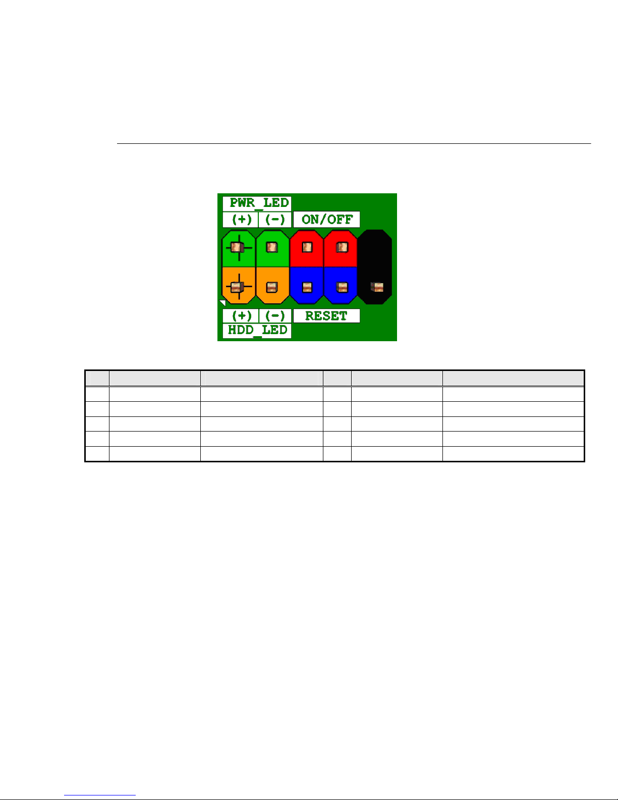
Front panel main header
Fi g u re 2 Fron t panel main he a d er pin-ou t
Pin Signal Name Description Pin Signal Name Description
1 HDD_POWER_LED Pull-up resistor (750) to +5V 2 POWER_LED_MAIN [Out] Front panel LED (main color)
3 HDD_LED# [Out] Hard disk activity LED 4 POWER_LED_ALT [Out] Front panel LED (alt color)
5 GROUND Ground 6 POWER_SWITCH# [In] Power switch
7 RESET_SWITCH# [In] Reset switch 8 GROUND Ground
9 +5V_DC Power 10 KEY No pin
T
AB LE 1 FRO N T P A NEL MAI N H E ADE R SI G NAL S
Page 8
8
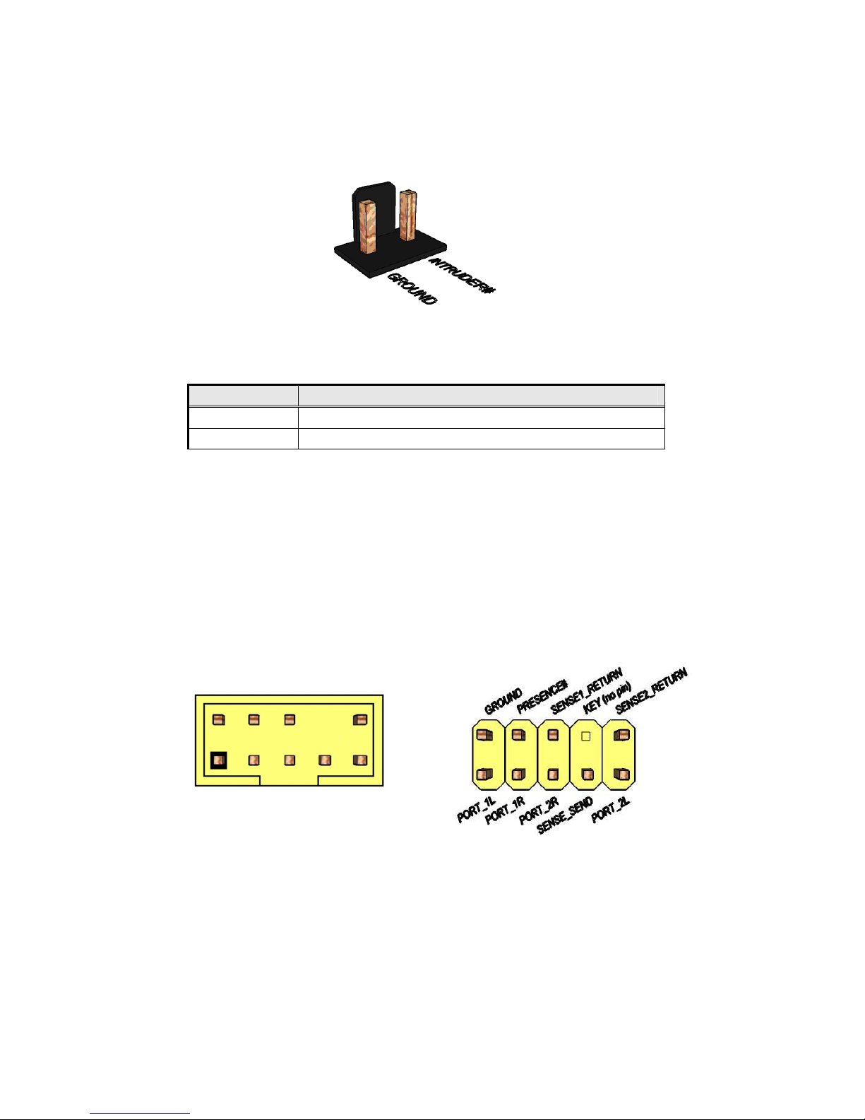
Chassis Intrusion Detection Header
The chassis intrusion detection header must be 1x2, 2.54mm pitch, colored black
and with extended back, as defined in below
Fi g u re 3 Chassi s intrusion detection h e a der
Pin Signal Name
1
Intrusion Detection
2 Ground
T
AB LE 3 CHA S SIS I NT R USI ON D ETE C TION HE A DER SIG NALS
HD Audio front panel audio head er
Fi g u re 4 HD Audi o front pane l audio hea d e r pin-out di agram
Page 9

9
Pin Signal name Description
1 PORT 1L
Analog Port 1 - Left channel (Microphone)
2 GND
Ground
3 PORT 1R
Analog Port 1 - Right channel (Microphone)
4 PRESENCE#
Active low signal that signals BIOS that an Intel® HD Audio dongle is connected to
the analog header. PRESENCE# = 0 when an Intel® HD Audio dongle is connected.
5 PORT 2R
Analog Port 2 - Right channel (Headphone)
6 SENSE1 RETURN
Jack detection return for front panel (JACK1)
7 SENSE SEND
Jack detection sense line from the Intel® HD Audio CODEC jack detection resistor
network
8 KEY
No pin
9 PORT 2L
Analog Port 2 - Left channel (Headphone)
10 SENSE2 RETURN
Jack detection return for front panel (JACK2)
T
AB L E 4 HD AUD IO F R ON T PA N EL A UDI O H E ADE R
Page 10
10
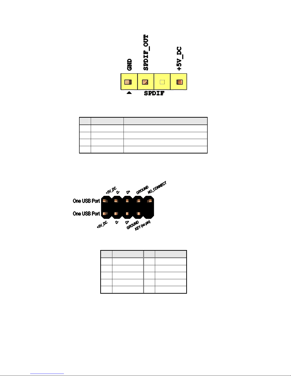
Internal SPDIF header
Fi g u re 5 Int e r n a l SPDIF he ad e r pin-out diagram
Pin Signal name Description
1 GND Ground
2 SPDIF_OUT SPDIF signal from the codec
3 Key (no pin) Key (no pin)
4 +5V_DC 5V power (for optical/TOSLINK module)
T
AB L E 5 INT E RNA L
SPD I F
H E ADE R
Front panel US B header
Fi g u re 6 Fr on t panel U SB h e ader pi n- o u t
Pin Signal Pin Signal
1 +5V DC 2 +5V DC
3 Data (negative) 4 Data (negative)
5 Data (positive) 6 Data (positive)
7 Ground 8 Ground
9 Key (no pin) 10 No Connect
T
AB L E 6 FRO N T P A NEL
USB
H E ADE R SI G NALS
Page 11

11
Parallel port h eader
Fi g u re 7 Par a l lel port h e a der pin- o ut
Pin Standard Signal Name ECP Signal Name EPP Signal Name
1 STROBE# STROBE# WRITE#
2 AUTOFD# AUTOFD#, HOSACK DATASTB#
3 PD0 PD0 PD0
4 FAULT# FAULT#, PERIPHREQST# FAULT#
5 PD1 PD1 PD1
6 INT# INT#, REVERSERQST# RESET#
7 PD2 PD2 PD2
8 SLCTIN# SLCTIN# ADDRSTB#
9 PD3 PD3 PD3
10 GROUND GROUND GROUND
11 PD4 PD4 PD4
12 GROUND GROUND GROUND
13 PD5 PD5 PD5
14 GROUND GROUND GROUND
15 PD6 PD6 PD6
16 GROUND GROUND GROUND
17 PD7 PD7 PD7
18 GROUND GROUND GROUND
19 ACK# ACK# INTR
20 GROUND GROUND GROUND
21 BUSY BUSY#, PERIPHACK WAIT#
22 GROUND GROUND GROUND
23 PERROR PE, ACKREVERSE# PE
24 GROUND GROUND GROUND
25 SELECT SELECT SELECT
26 KEY (no pin) KEY (no pin) KEY (no pin)
T
AB LE 7 PAR A LLE L PO R T H EADE R S I G NAL S
Page 12
12
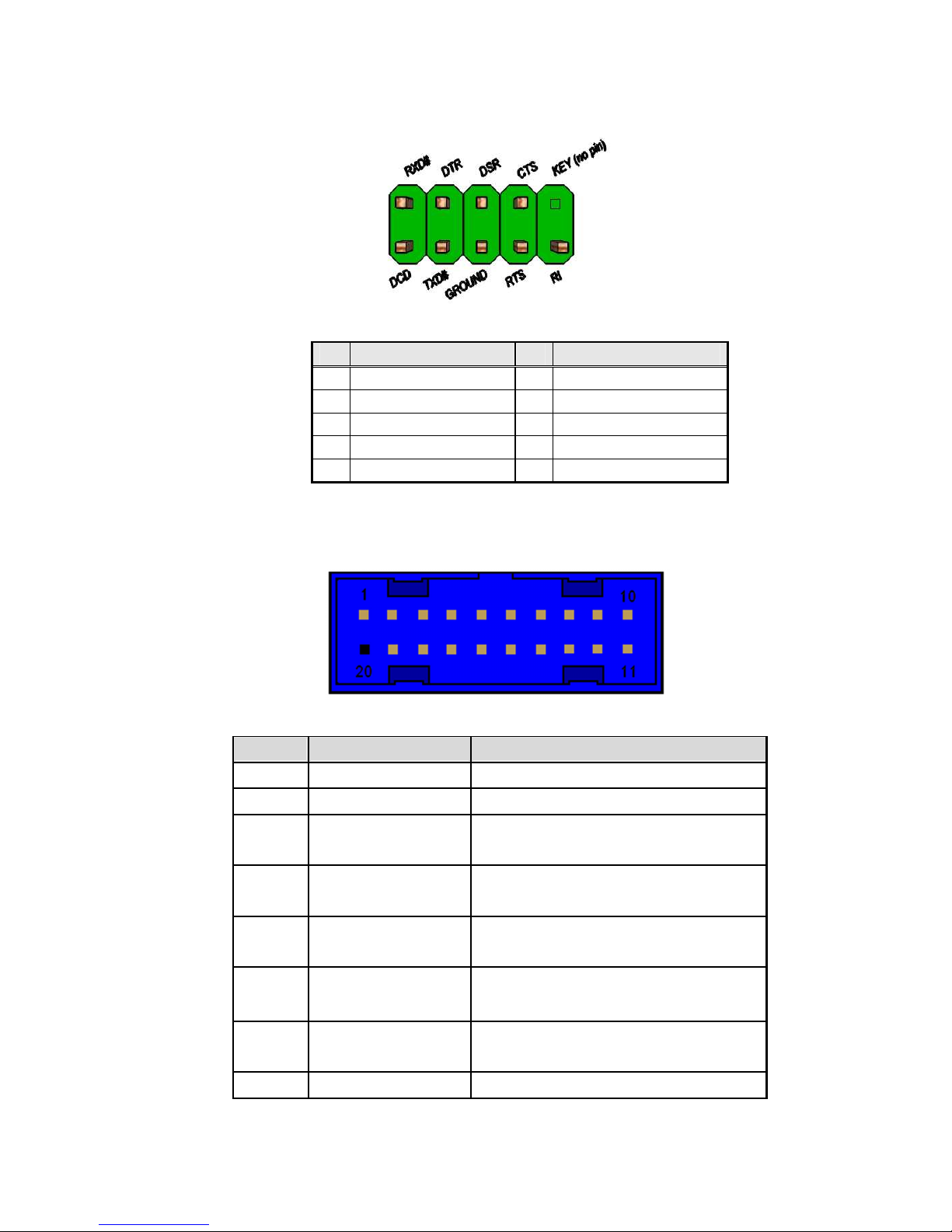
Serial port header
Fi g u re 8 Seri a l port he a d e r pin-ou t
Pin Signal Pin Signal
1 DCD (Data Carrier Detect) 2 RXD# (Receive Data)
3 TXD# (Transmit Data) 4 DTR (Data Terminal Ready)
5 Ground 6 DSR (Data Set Ready)
7 RTS (Request To Send) 8 CTS (Clear To Send)
9 RI (Ring Indicator) 10 Key (no pin)
T
AB L E 8 SER I A L P ORT H EAD ER S I GNA LS
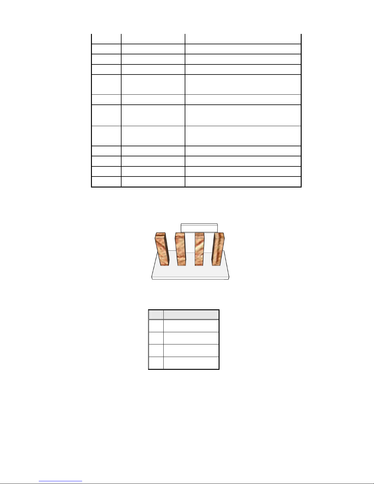
Front Panel US B 3.0 header
Fi g u re 9: F r o n t Panel U S B 3.0 header
PIN Signal Description
1 Vbus Power
2 IntA_P1_SSRX- USB3 ICC Port1 SuperSpeed Rx-
3 IntA_P1_SSRX+
USB3 ICC Port1 SuperSpeed Rx+
Data (positive)
4 GND
Ground
Ground
5 IntA_P1_SSTX-
USB3 ICC Port1 SuperSpeed TxNo Connect
6 IntA_P1_SSTX+ USB3 ICC Port1 SuperSpeed Tx+
7 GND
Ground
Ground
8 IntA_P1_D- USB3 ICC Port1 D- (USB2 Signal D-)
Page 13
13
9 IntA_P1_D+ USB3 ICC Port1 D- (USB2 Signal D+)
10 ID Over Current Protection
11 IntA_P2_D+ USB3 ICC Port2 D+ (USB2 Signal D+)
12 IntA_P2_D- USB3 ICC Port2 D- (USB2 Signal D-)
13 GND
Ground
Ground
14 IntA_P2_SSTX+ USB3 ICC Port2 SuperSpeed Tx+
15 IntA_P2_SSTX- USB3 ICC Port2 SuperSpeed Tx-
16 GND
Ground
Ground
17 IntA_P2_SSRX+ USB3 ICC Port2 SuperSpeed Rx+
18 IntA_P2_SSRX- USB3 ICC Port2 SuperSpeed Rx19 Vbus Power
20 Key Not Connected
T
AB LE 9: FRO NT PAN EL
USB3.0
H E ADE R SI G NAL
Processor fan header
Fi g u re 10: Pr oc essor fa n h eader
Pin Signal
4
FAN_CTRL
3
FAN_TACH
2
VCC-12V
1
GND
T
AB LE
10: P
ROC E SSO R FA N H E ADE R
Page 14
14
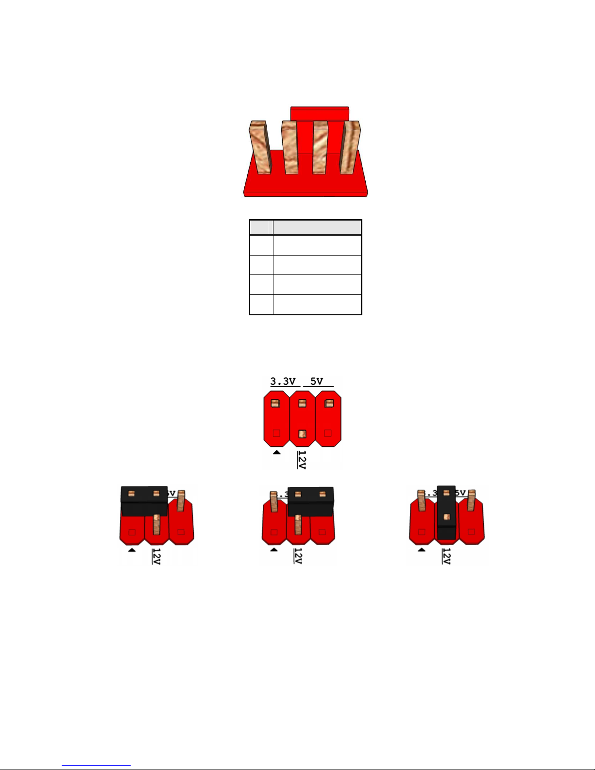
Front/Rear fan header
Fi g u re 11: Fr on t /Re ar fan h e a d er
T
AB L E
11: P
ROC E SSO R FA N H E ADE R
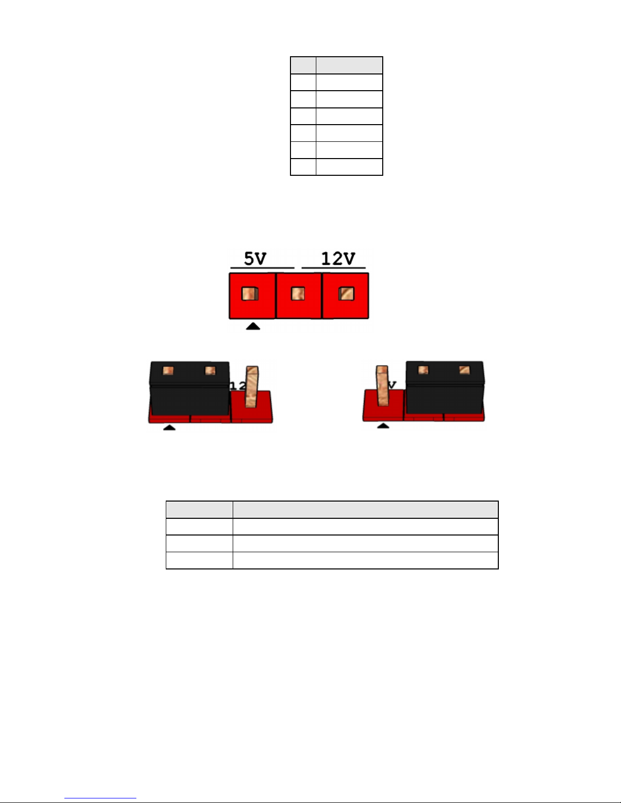
LVDS panel voltage selection header
Pins 2&4: jumper position for 3.3V Pins 6&4: jumper position for 5V Pins 3&4: jumper position for 12V
Fi g u re 12: LVD S p anel vol t a g e sele ct i on header
Pin Signal
4
FAN_CTRL
3
FAN_TACH
2
VCC-12V
1
GND
Page 15
15
Pin Signal Name
1 NC
2 VCC3/3V
3 12V
4 LCD SEL PWR
5 NC
6 VCC/5V
T
AB L E
12 : LVD S
P A NEL V OL T A GE SELE C TI O N H E ADE R
Inverter po wer voltage selection header
Pins 1&2: jumper position for 5V Pins 3&2: jumper position for 12V
Fi g u re 13: In v e rter power v o ltage sele c ti on heade r
Pin Signal Name
1 VCC/5V
2 BKLT_PWR
3 12V
T
AB LE
13: I
NV E RTE R PO WER VOL T AGE SELE CTI O N H EADE R
Page 16

16
LVDS
Pin Signal Name Description
1 BKLT_EN Backlight enable
2 BKLT_PWM Backlight PWM control
3 5V/12V Inverter power
4 5V/12V Inverter power
5 GND Ground
6 GND Ground
7 BRIGHTNESS_UP BRIGHTNESS UP
8 BRIGHTNESS_DOWN BRIGHTNESS DOWN
T
AB L E
14 : 8-
PI N
LV D S
I N VE R T ER POWE R H E ADE R PI N-OUT RE F E RE N CE
Pin Signal Description
1 LA_DATAP3 LVDS Channel A diff data output - positive
2 LA_DATAN3 LVDS Channel A diff data output - negative
3 LA_DATAP2 LVDS Channel A diff data output - positive
4 LA_DATAN2 LVDS Channel A diff data output - negative
5 LA_DATAP1 LVDS Channel A diff data output - positive
6 LA_DATAN1 LVDS Channel A diff data output - negative
7 LA_DATAP0 LVDS Channel A diff data output - positive
8 LA_DATAN0 LVDS Channel A diff data output - negative
9 LB_DATAP3 LVDS Channel B diff data output-positive
10 LB_DATAN3 LVDS Channel B diff data output-negative
11 LB_DATAP2 LVDS Channel B diff data output-positive
12 LB_DATAN2 LVDS Channel B diff data output-negative
13 LB_DATAP1 LVDS Channel B diff data output-positive
14 LB_DATAN1 LVDS Channel B diff data output-negative
15 LB_DATAP0 LVDS Channel B diff data output-positive
16 LB_DATAN0 LVDS Channel B diff data output-negative
17 GND Ground
18 3.3V/5V/12V Selectable LCD power output
19 3.3V/5V/12V Selectable LCD power output
20 3.3V/5V/12V Selectable LCD power output
21 NC NC
22 EDID_3.3V VCC3
23 GND Ground
24 GND Ground
25 GND Ground
26 LA_CLKP LVDS Channel A diff data output - positive
Page 17
17
27 LA_CLKN LVDS Channel A diff data output - negative
28 GND Ground
29 GND Ground
30 GND Ground
31 EDID_CLK EDID/DDC clock signal
32 BKLT_EN
33 BKLT_CTRL
34 LB_CLKP LVDS Channel B diff data output - positive
35 LB_CLKN LVDS Channel B diff data output - negative
36 BKLT_PWR Selectable BKLT power output
37 BKLT_PWR Selectable BKLT power output
38 BKLT_PWR Selectable BKLT power output
39 NC NC
40 EDID_DATA EDID/DDC data signal
T
AB LE
15: 40-
PI N
LVD S
D ATA H EADE R P I N-OU T RE FERE NCE
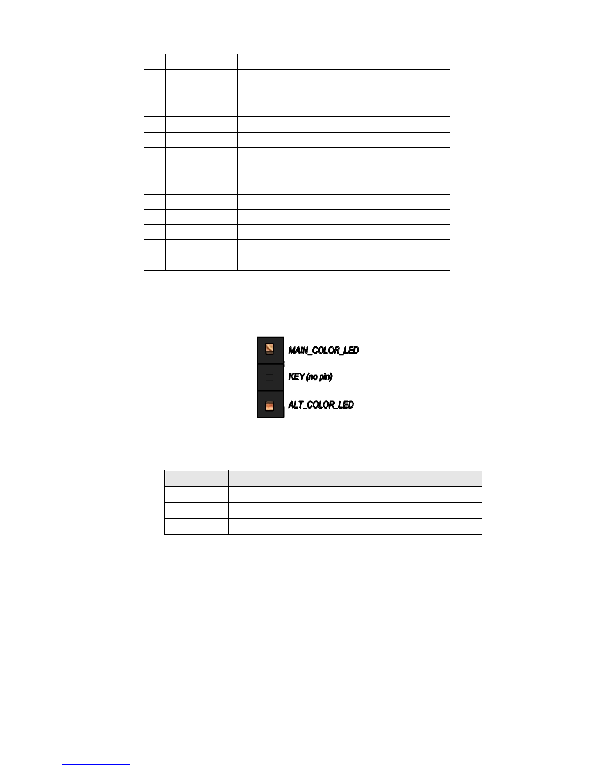
Alternate Powe r LED header
Figure 14 Alternate Power LED header
Pin Signal Name
1 MAIN COLOR LED
2 KEY
3 ALT COLOR LED
T
AB LE
16: A
LT E RNAT E POWE R
LE D
H E ADE R
Page 18
18
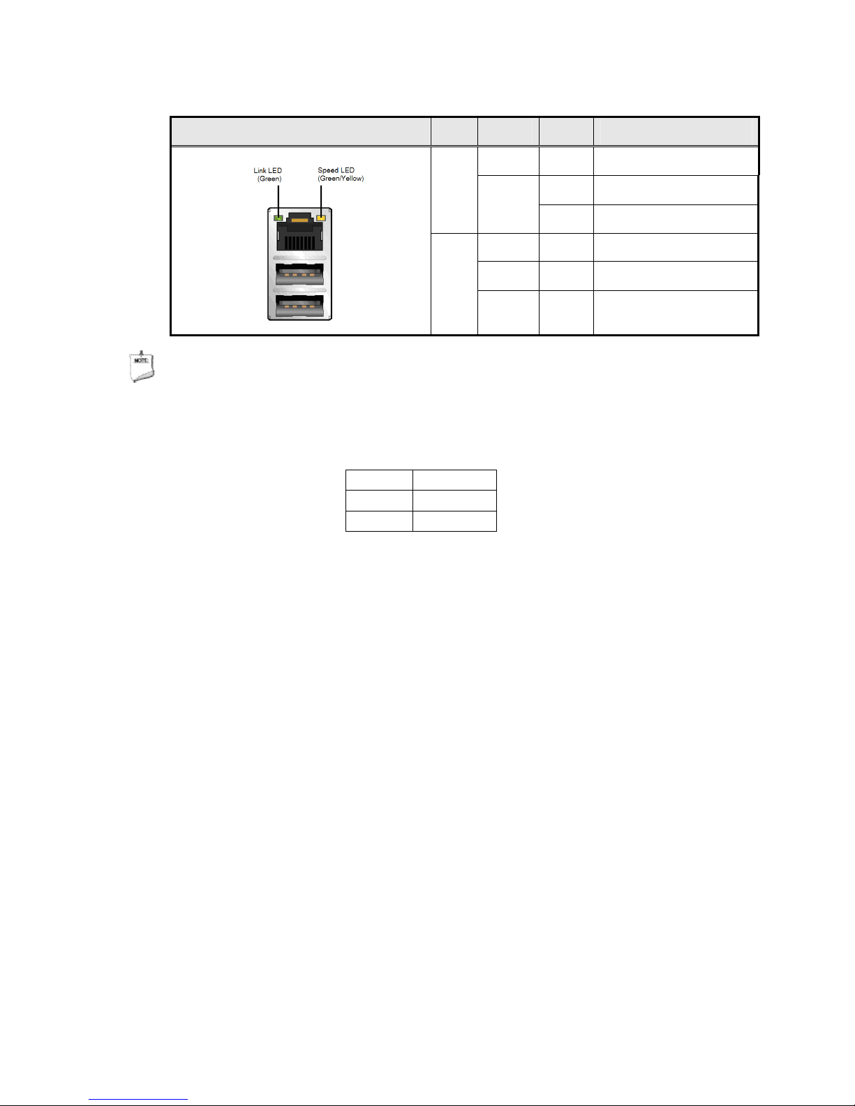
RJ45 LED Behavior
Diagram LED Color State Condition
Link
N/A Off LAN link is not established
Green
On LAN link is established
Blinking LAN activity occurring
Speed
N/A Off 10 Mb/s data rate
Green On 100 Mb/s data rate
Yellow On 1000 Mb/s data rate
T
AB LE
17:
RJ45 LED
B E HAV I OR
Note: LAN solution must be tested for IEEE802.3 conformance.
CMOS Clear
CMOS Clear
1-2 Normal
2-3 Clear CMOS
T
AB L E
18 :
CM O S C
LE A R B E HAV I OR
Page 19

19
MITAC Desktop Board PH10LU
BIOS Specifiction
Page 20

20
GENERAL OVERVIEW
This document specifies the BIOS requirements for PH10LU
Note: The BIOS specification may be changed depend on hardware design. This is based on the
product specification document (PRD).
HARDWARE OVERVIEW
CPU
- Intel Haswell Series.
- Socket Type: LGA1150
System Memory
- 4 slots UDIMM with DDR3 1066/1333/1600MHz (By Intel processor specification)
Chipset
- Intel Lynx Point Q87
BIOS ROM
- 64Mbit SPI Flash ROM + 32Mbit SPI Flash ROM
Super I/O
- Nuvoton NCT6104
Keyboard/Mouse
- Standard USB Devices, PS2 swap
Storage
- SATA HDD
Graphics
- Intel HD Graphic
- 1920x1080p Panel (Option), 1x DP, 1x DVI-I
Audio
- Intel HD audio, Realtek ALC888 and ALC662 Codec co-design
LAN
- Intel Clarkville I217-LM and Intel Springville I210-AT (Optional)
Add-in Slot
- Slot 5 – PCIe 3.0 x16
- Slot 3 – PCIe 2.0 x1 (Either one with Mini card slot)
- Slot 2 – PCIe 2.0 x1
- Slot 1 – PCIe 2.0 x4
- Mini PCIe slot *1 (Either one with Slot3)
TPM(Optional)
- WPCT210I
Internal Header
- SATA 6.0Gb Header X 6
- Dual Port USB 2.0 Header x2
- Dual Port USB 3.0 Header x1
- Serial Port Header x2
- Parallel Port Header X1
Page 21
21
- Chassis Intrusion Header x1
- Audio Header (Front Panel Mic / Hp)
- S/PDIF Out Audio Header
- 4-pin CPU Fan Header
- 4-pin Front Fan Header
- 4-pin Rear Fan Header
External I/O
- USB 2.0 x4
- USB 3.0 x2
- PS2 x1
- Serial Port x2
- RJ45 x1
- 3-stack Audio Jack
Supporting OS
- Windows 7
- Windows 8 32-bit(UEFI,CSM Enabled) / Windows 8 64-Bit(Native UEFI)
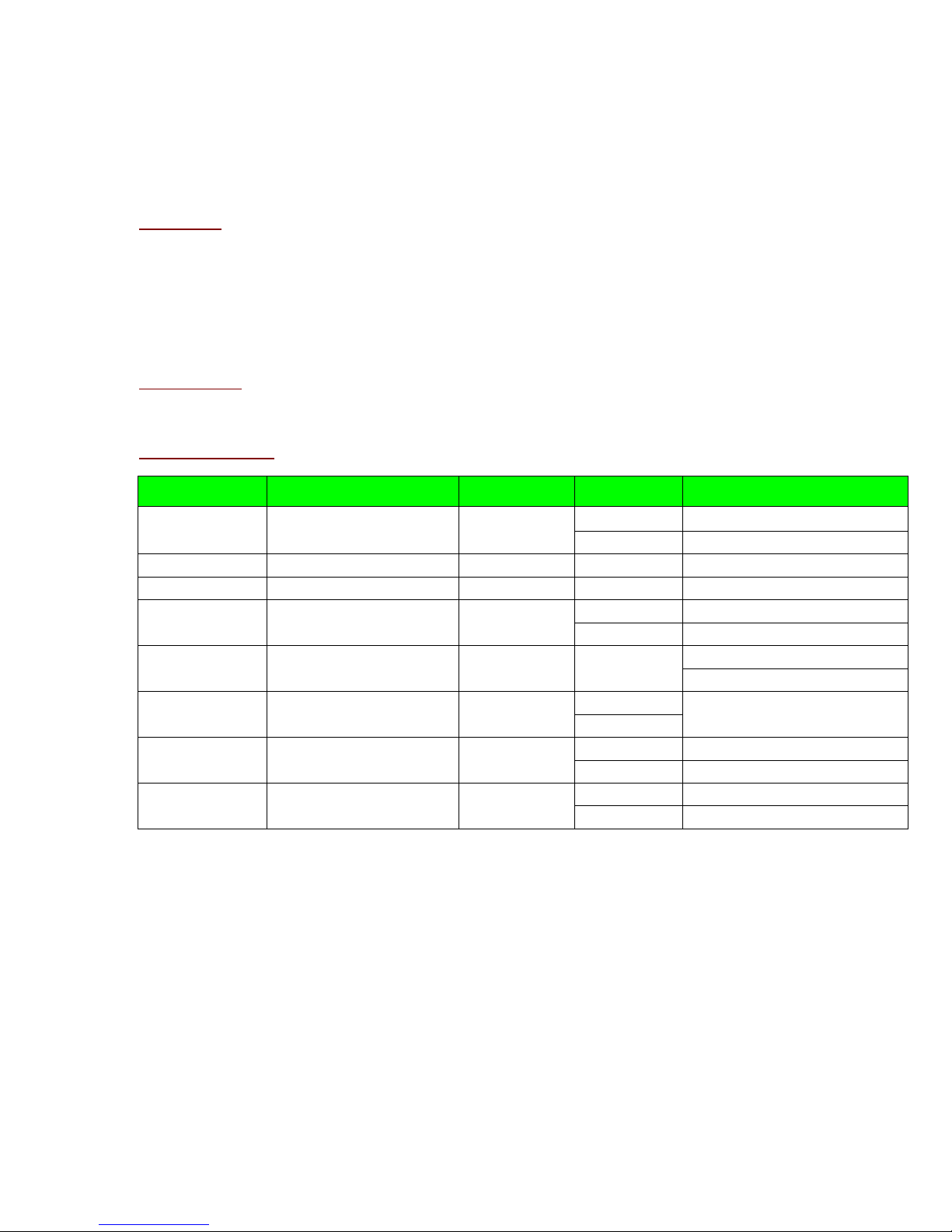
GPIO Pin Definition
GPIO Pin Name Net Name Configure Initial value BIOS Function Description
GPIO0 FRONT_AUDIO_DET GPI
Low No FP Audio Panel
High FP Audio Panel is present
GPIO6 BRIGHTNESS_UP_R GPO Low GPO Low Brightness up function
GPIO7 BRIGHTNESS_DOWN_R GPO Low GPO Low Brightness down function
GPIO12 LAN1_DISABLE_N GPO
Low Disable I217 LAN
High Enable I217 LAN
GPIO31 STBY_LED_CTRL GPO
Low S0 State
High S3 State
GPIO32 MINI_CARD_DISABLE_ GPO
Low Disable Mini Card
High Enable Mini Card
GPIO34 EDID_ISO_N GPO
Low Disable LVDS EDID EEPROM
High Enable LVDS EDID EEPROM
GPIO46 LAN2_DISABLE_N GPO
Low Disable I210 LAN
High Enable I210 LAN
REFERENCES
CPU Specification :
518491_EP_Haswell_SR_518491_rev0.5.pdf
487245_HSW_DT_EDS_Vol_1_Rev2_0.pdf
487247_HSW_EDS_Vol_2_Rev2_0.pdf
492662_492662_Haswell_SystemAgent_BS_1.5.pdf
Chipset Specification :
486708_486708_LPT_EDS_Rev1_0.pdf
486708_486708_LPT_EDS_Rev2_0.pdf
Page 22

22
Management Engine Specification :
493796_493796_Revision_1p2_ME9_0_5MB.pdf
Super I/O Specification :
NCT6104D_Datasheet_v1_5.pdf
Others :
368119_Intel®_Graphics_Media_Accelerator–Binary_Modification_Program_User’s_Guide_Rev2_5.pdf
Intel High Definition Audio (Programmers Reference Manual).pdf
503098_UEFI_Graphics_Output_Protocol_Driver_BIOS_Integration_Guide_Rev_1_0.pdf
BIOS OVERVIEW
AMI APTIO 4.6.5.3 BIOS, UEFI Version = 2.3.1 , PI Version = 1.2
Code Base : 1AQQW026
Support Platform : Intel Shark-Bay
Support IGD VBIOS : 2171 / Intel GOP VBIOS : 165
Provide BIOS Setup Utility
Support Advanced Configuration and Power Interface (ACPI 2.0 or later)
Support DMI 2.3.1 or later
Support BIOS Boot Specification 1.01 or higher
Support Plug and Play 1.0a, PCI Express 1.0a
Support USB 1.1 / 2.0 / 3.0
Support USB wake up from S3
Support Advanced Hard disk Features (Not support HDD security)
Support USB legacy (Keyboard & Mouse & Floppy & CD-ROM)
Support Wake on LAN
Support Boot Control Features (Boot devices sequence selections)
Support Security password: BIOS Setup Administrator and User password
Support OEM Activation 3.0
Support PXE boot..
Support RTC wake up from S3/S4/S5
Support Intel Rapid Start Technology
Support FAN Control
Support Trusted Computing
Support Intel vPro
POST
OVERVIEW
When a computer is turned on, the BIOS runs a Power-On Self Test (POST). Program
execution start at memory location F000:FFF0h. This address is part of ROM BIOS and
contains a jump command to a series of BIOS routines that test and initialize the hardware
components. POST consists of various test and initialization routines for chipset’ processor
and hardware components. When all test have been performed and components have been
Page 23
23
initialized, control is transferred to the INT 19h Bootstrap Loader, to load the available
operating system on the disk. During the POST period, a value form 00h through FFh is
written to the manufacturing test port (generally is I/O port 80h). These values are known as
POST Diagnostic Codes. (refer to appendix in detail)
SPLASH SCREEN
POST Logo: N/A
HOT KEY OPTIONS
Hot keys should be accepted during POST. The following Hot Keys are required at boot time.
DEL => Enter BIOS setup utility.
F7 =>Popup boot menu. The user will be presented with a list of boot options that they may
select a device to boot from (i.e., override the existing boot list for that particular boot).
BIOS WARNING EVENT LIST
Event Warning Message
POST Memory not detect Three long beep code
POST CPU fan rpm not detect Show Message “WARNING: CPU FAN Not Found. Continue after 10 seconds.”
BIOS SETUP UTILITY
During POST, the end user can press <DEL> to enter Setup and change the system parameters
originally specified in the BIOS defaults. The Setup items are described in BIOS Setup Specification.
BIOS Setup Specification for detail.
POWER MANAGEMENT
ACPI (ADVANCED CONFIGURATION AND POWER INTERFACE)
Overview
ACPI 2.0 or later compatibility.
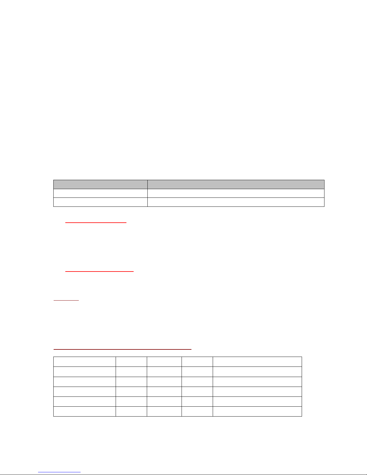
System support Full on state (S0), Suspend to RAM (STR - S3), Hibernation/Suspend to Disk (STD S4), Soft Off (S5)
System Power States and Wakeup Event Resource
S3 S4 S5 DeepSleep Enabled in S4-S5
USB Keyboard/Mouse Yes No No No
RTC Yes Yes Yes Yes
Wake on LAN (WOL) Yes Yes Yes No
Power Button Yes Yes Yes Yes
PS2 Keyboard/Mouse Yes No No No
Page 24

24
Power Button
In ACPI mode, Power Button switches the system from the sleeping/soft off state to the working state,
and signals the OS to transition to a sleeping state from the working state. In NON ACPI mode, Power
button is only to turn on/off system.
SUBSYSTEM ID OVERVIEW
The purpose of Subsystem Vendor ID and the Subsystem Device ID is further identifying the PCI
device. The Subsystem Vendor ID is that of the board/card manufacturer. The Subsystem Device ID is
assigned by the subsystem vendor.
For on-brand board/system, BIOS needs to configure MiTAC SVID as manufacturer ID (to identify for
DTM verification) & SSID (used project code).
Name
M870 Value (Hex)
SVID
1071
SSID
0727
DMI/SMBIOS OVERVIEW
Desktop Management Interface (DMI) / System Management BIOS (SMBIOS) is a method of
managing computers in an enterprise. The main component of DMI/SMBIOS is the Management
Information Format Database. This database contains all the information about the computing system
and its components. Using DMI/SMBIOS, a system administrator can obtain the types, capabilities,
operational status, installation date, and other information about the system components.
[System Information] (Type 1)
Manufacturer (String1) - "MiTAC"
Product Name (String2) - "PH10LU"
Version (String3) - " "
Serial Number (String4) - " "
UUID: 0x00 0x02 0x00 0x03 0x00 0x04 0x00 0x05 0x00 0x06 0x00 0x07 0x00 0x08 0x00 0x09
Wakeup Type: 0x06 - Power Switch
SKU Number (String5) - " "
[Base Board Information] (Type 2)
Manufacturer (String1) - "MiTAC"
Product (String2) - "PH10LU"
Version (String3) - " "
Serial Number (String4) - " "
Asset Tag (String5) - " "
Board Type: 0x0A - Motherboard (includes processor, memory, and I/O)
[System Enclosure or Chassis] (Type 3)
Manufacturer (String1) - "MiTAC"
Enclosure Type: 0x03 - Desktop
Page 25

25
Version (String2) - " "
Serial Number (String3) - " "
Asset Tag Number (String4) - " "
Boot-up State: 0x03 - Safe
Power Supply State: 0x03 - Safe
Thermal State: 0x03 - Safe
Security State: 0x03 - None
OEM-defined: 0x00000000
Height: 0x00 (0)
Number of Power Cords: 0x01 (1)
Contained Element Count: 0x00 (0)
Element Record Length: 0x00 (0)
SKU Number (String5) - " "
UTILITIES
BIOS FLASH
If BIOS supports multi BIOS ROM, the flash utility should support them.
Vender Name Model Name
Winbond W25Q64BV
Winbond W25Q32FV
MXIC MX25L6475
MXIC MX25L3273
BIOS RELEASE
BIOS REVISION
MiTAC BIOS Naming:
D727 0 A 01
SKU B/C 1 2 3
1: Sku ID; “0” for MiTAC
2: Stage;
X =>Develop Stage.
T =>Test Stage.
A =>Production Stage
3: Version number (Decimal);
RELEASE COMPONENT
Release BIOS ROM and Flash Utility for each BIOS release. If Flash Utility is not modified, may not
release Flash Tool. Enforce the virus check of the release component.
Page 26

26
Send Release Note for each BIOS release.
Release Note contains added features, fixed issues & known restriction.
BIOS RELEASE
FTP Server
PLM
EMAIL
DISTRIBUTION LIST FOR BIOS RELEASE
Customer, RD, CAD, QA.
BIOS RELEASE NOTE FORMAT
//********************************************************************************
// Revision No. :
// Build Date :
// ME Version :
// GbE PHY :
// GbE Option Rom Version :
// VBIOS Version :
// GOP Driver Version :
// Checksum :
// Haswell MRC Version :
//********************************************************************************
// MicroCode revision & CPU Support List :
// M32306C1_FFFF0013("Intel(R) Haswell Processor A-0")
// M32306C2_FFFF0006("Intel(R) Haswell Processor B-0")
// M32306C3_00000009("Intel(R) Haswell Processor C-0")
//********************************************************************************
// Reference Code revision :
// Haswell reference code ver.
// NorthBridge Haswell - SystemAgent: reference code ver.
// SouthBridge LynxPoint: reference code label ver.
// Haswell PowerManagement PPM Intel Reference code ver.
// Haswell ACPI Reference code ver.
// Manageability Engine (ME) reference code ver.
// Fast Flash Standby (FFS) reference code ver.
//********************************************************************************
Release History:
QUALITY
Page 27

27
MAINTENANCE
Support new function and new OS in nearly future as many as possible
Support simple changing from our customer’s BIOS requests.
For example,
- Change the default value in BIOS Setup
- Change the boot device order in BIOS Setup.
BIOS QA TEST
Must to PASS below tests before release
BIOS version (correct version)
BIOS Setup (including "Restore Defaults", "Discard Changes" and clear CMOS) (follow spec)
S3/S4/S5 power cycling tests over 100 times (without any error)
Hot Keys (function normal)
Windows Device manager (no “!”)
BIOS Flash (successful & check correct BIOS version, Setup without changes & no “!” in Windows
device manager)
Fixed Bugs (verified okay)
Regression tests
APPENDIX
POST Diagnostic Codes
Status Code Ranges
Status Code Range Description
0x01 – 0x0F SEC Status Codes & Errors
0x10 – 0x2F PEI execution up to and including memory detection
0x30 – 0x4F PEI execution after memory detection
0x50 – 0x5F PEI errors
0x60 – 0xCF DXE execution up to BDS
0xD0 – 0xDF DXE errors
0xE0 – 0xE8 S3 Resume (PEI)
0xE9 – 0xEF S3 Resume errors (PEI)
0xF0 – 0xF8 Recovery (PEI)
0xF9 – 0xFF Recovery errors (PEI)
Standard Status Codes
SEC Status Codes
Status Code Description
0x0 Not used
Progress Codes
0x1 Power on. Reset type detection (soft/hard).
Page 28

28
0x2 AP initialization before microcode loading
0x3 North Bridge initialization before microcode loading
0x4 South Bridge initialization before microcode loading
0x5 OEM initialization before microcode loading
0x6 Microcode loading
0x7 AP initialization after microcode loading
0x8 North Bridge initialization after microcode loading
0x9 South Bridge initialization after microcode loading
0xA OEM initialization after microcode loading
0xB Cache initialization
SEC Error Codes
0xC – 0xD Reserved for future AMI SEC error codes
0xE Microcode not found
0xF Microcode not loaded
SEC Beep Codes
None
PEI Status Codes
Status Code Description
Progress Codes
0x10 PEI Core is started
0x11 Pre-memory CPU initialization is started
0x12 Pre-memory CPU initialization (CPU module specific)
0x13 Pre-memory CPU initialization (CPU module specific)
0x14 Pre-memory CPU initialization (CPU module specific)
0x15 Pre-memory North Bridge initialization is started
0x16 Pre-Memory North Bridge initialization (North Bridge module specific)
0x17 Pre-Memory North Bridge initialization (North Bridge module specific)
0x18 Pre-Memory North Bridge initialization (North Bridge module specific)
0x19 Pre-memory South Bridge initialization is started
0x1A Pre-memory South Bridge initialization (South Bridge module specific)
0x1B Pre-memory South Bridge initialization (South Bridge module specific)
0x1C Pre-memory South Bridge initialization (South Bridge module specific)
0x1D – 0x2A OEM pre-memory initialization codes
0x2B Memory initialization. Serial Presence Detect (SPD) data reading
0x2C Memory initialization. Memory presence detection
0x2D Memory initialization. Programming memory timing information
0x2E Memory initialization. Configuring memory
0x2F Memory initialization (other).
0x30 Reserved for ASL (see ASL Status Codes section below)
0x31 Memory Installed
0x32 CPU post-memory initialization is started
0x33 CPU post-memory initialization. Cache initialization
0x34 CPU post-memory initialization. Application Processor(s) (AP) initialization
0x35 CPU post-memory initialization. Boot Strap Processor (BSP) selection
Page 29

29
0x36 CPU post-memory initialization. System Management Mode (SMM) initialization
0x37 Post-Memory North Bridge initialization is started
0x38 Post-Memory North Bridge initialization (North Bridge module specific)
0x39 Post-Memory North Bridge initialization (North Bridge module specific)
0x3A Post-Memory North Bridge initialization (North Bridge module specific)
0x3B Post-Memory South Bridge initialization is started
0x3C Post-Memory South Bridge initialization (South Bridge module specific)
0x3D Post-Memory South Bridge initialization (South Bridge module specific)
0x3E Post-Memory South Bridge initialization (South Bridge module specific)
0x3F-0x4E OEM post memory initialization codes
0x4F DXE IPL is started
PEI Error Codes
0x50 Memory initialization error. Invalid memory type or incompatible memory speed
0x51 Memory initialization error. SPD reading has failed
0x52 Memory initialization error. Invalid memory size or memory modules do not match.
0x53 Memory initialization error. No usable memory detected
0x54 Unspecified memory initialization error.
0x55 Memory not installed
0x56 Invalid CPU type or Speed
0x57 CPU mismatch
0x58 CPU self test failed or possible CPU cache error
0x59 CPU micro-code is not found or micro-code update is failed
0x5A Internal CPU error
0x5B reset PPI is not available
0x5C-0x5F Reserved for future AMI error codes
S3 Resume Progress Codes
0xE0 S3 Resume is stared (S3 Resume PPI is called by the DXE IPL)
0xE1 S3 Boot Script execution
0xE2 Video repost
0xE3 OS S3 wake vector call
0xE4-0xE7 Reserved for future AMI progress codes
0xE0 S3 Resume is stared (S3 Resume PPI is called by the DXE IPL)
S3 Resume Error Codes
0xE8 S3 Resume Failed in PEI
0xE9 S3 Resume PPI not Found
0xEA S3 Resume Boot Script Error
0xEB S3 OS Wake Error
0xEC-0xEF Reserved for future AMI error codes
Recovery Progress Codes
0xF0 Recovery condition triggered by firmware (Auto recovery)
0xF1 Recovery condition triggered by user (Forced recovery)
0xF2 Recovery process started
0xF3 Recovery firmware image is found
0xF4 Recovery firmware image is loaded
0xF5-0xF7 Reserved for future AMI progress codes
Page 30

30
Recovery Error Codes
0xF8 Recovery PPI is not available
0xF9 Recovery capsule is not found
0xFA Invalid recovery capsule
0xFB – 0xFF Reserved for future AMI error codes
PEI Beep Codes
Status Code Description
0x53 Three long beep - Memory initialization error. No usable memory detected
DXE Status Codes
Status Code Description
0x60 DXE Core is started
0x61 NVRAM initialization
0x62 Installations of the South Bridge Runtime Services
0x63 CPU DXE initialization is started
0x64 CPU DXE initialization (CPU module specific)
0x65 CPU DXE initialization (CPU module specific)
0x66 CPU DXE initialization (CPU module specific)
0x67 CPU DXE initialization (CPU module specific)
0x68 PCI host bridge initialization
0x69 North Bridge DXE initialization is started
0x6A North Bridge DXE SMM initialization is started
0x6B North Bridge DXE initialization (North Bridge module specific)
0x6C North Bridge DXE initialization (North Bridge module specific)
0x6D North Bridge DXE initialization (North Bridge module specific)
0x6E North Bridge DXE initialization (North Bridge module specific)
0x6F North Bridge DXE initialization (North Bridge module specific)
0x70 South Bridge DXE initialization is started
0x71 South Bridge DXE SMM initialization is started
0x72 South Bridge devices initialization
0x73 South Bridge DXE Initialization (South Bridge module specific)
0x74 South Bridge DXE Initialization (South Bridge module specific)
0x75 South Bridge DXE Initialization (South Bridge module specific)
0x76 South Bridge DXE Initialization (South Bridge module specific)
0x77 South Bridge DXE Initialization (South Bridge module specific)
0x78 ACPI module initialization
0x79 CSM initialization
0x7A – 0x7F Reserved for future AMI DXE codes
0x80 – 0x8F OEM DXE initialization codes
0x90 Boot Device Selection (BDS) phase is started
0x91 Driver connecting is started
0x92 PCI Bus initialization is started
0x93 PCI Bus Hot Plug Controller Initialization
0x94 PCI Bus Enumeration
0x95 PCI Bus Request Resources
Page 31

31
0x96 PCI Bus Assign Resources
0x97 Console Output devices connect
0x98 Console input devices connect
0x99 Super IO Initialization
0x9A USB initialization is started
0x9B USB Reset
0x9C USB Detect
0x9D USB Enable
0x9E – 0x9F Reserved for future AMI codes
0xA0 IDE initialization is started
0xA1 IDE Reset
0xA2 IDE Detect
0xA3 IDE Enable
0xA4 SCSI initialization is started
0xA5 SCSI Reset
0xA6 SCSI Detect
0xA7 SCSI Enable
0xA8 Setup Verifying Password
0xA9 Start of Setup
0xAA Reserved for ASL (see ASL Status Codes section below)
0xAB Setup Input Wait
0xAC Reserved for ASL (see ASL Status Codes section below)
0xAD Ready To Boot event
0xAE Legacy Boot event
0xAF Exit Boot Services event
0xB0 Runtime Set Virtual Address MAP Begin
0xB1 Runtime Set Virtual Address MAP End
0xB2 Legacy Option ROM Initialization
0xB3 System Reset
0xB4 USB hot plug
0xB5 PCI bus hot plug
0xB6 Clean-up of NVRAM
0xB7 Configuration Reset (reset of NVRAM settings)
0xB8 – 0xBF Reserved for future AMI codes
0xC0 – 0xCF OEM BDS initialization codes
DXE Error Codes
Status Code Description
0xD0 CPU initialization error
0xD1 North Bridge initialization error
0xD2 South Bridge initialization error
0xD3 Some of the Architectural Protocols are not available
0xD4 PCI resource allocation error. Out of Resources
0xD5 No Space for Legacy Option ROM
0xD6 No Console Output Devices are found
0xD7 No Console Input Devices are found
Page 32

32
0xD8 Invalid password
0xD9 Error loading Boot Option (LoadImage returned error)
0xDA Boot Option is failed (StartImage returned error)
0xDB Flash update is failed
0xDC Reset protocol is not available
DXE Beep Codes
None
ASL Status Codes
Status Code Description
0x01 System is entering S1 sleep state
0x02 System is entering S2 sleep state
0x03 System is entering S3 sleep state
0x04 System is entering S4 sleep state
0x05 System is entering S5 sleep state
0x10 System is waking up from the S1 sleep state
0x20 System is waking up from the S2 sleep state
0x30 System is waking up from the S3 sleep state
0x40 System is waking up from the S4 sleep state
0xAC System has transitioned into ACPI mode. Interrupt controller is in PIC mode.
0xAA System has transitioned into ACPI mode. Interrupt controller is in APIC mode.
OEM-Reserved Status Code Ranges
Status Code Description
0x5 OEM SEC initialization before microcode loading
0xA OEM SEC initialization after microcode loading
0x1D – 0x2A OEM pre-memory initialization codes
0x3F – 0x4E OEM PEI post memory initialization codes
0x80 – 0x8F OEM DXE initialization codes
0xC0 – 0xCF OEM BDS initialization codes
Page 33

33
Battery Caution
There is insufficient space on this Desktop Board to provide instructions for replacing
and disposing of the Lithium ion coin cell battery. For system safety certification, the
statement below or an equivalent statement is required to be permanently and legibly
marked on the chassis near the battery.
A suitable caution label is included with MiTAC Desktop Board PH10LU.
CAUTION
Risk of explosion if the battery is replaced with an incorrect type. Batteries should be
recycled where possible. Disposal of used batteries must be in accordance with local
environmental regulations.
For information about replacing the battery, go to page 39.
 Loading...