

Page 1

MITAC Desktop Board PD10AI
Product Guide
Page 2

Intel Apollo Lake Processor with integrated graphics (Compatible with
DIMM (or
M.2 (2242/2260/2280) with USB2.0 and SATA III signal
Desktop Board Features
This chapter briefly describes the features of Desktop Board PD10AI.
Below
to summarizes the major features of the Desktop Board.
Feature Summary
T
AB L E
: MITA C D
Form Factor
Processor Chipset
Main Memory
Audio Controller Realtek ALC283 audio codec
Expansion
Capability
External I/O
Internal I/O
S I/O Controller NCT6793D
LAN Support Intel I211-AT (10/100/1000 Mb/s) Ethernet LAN controller *2
BIOS • BIOS resident in a Serial Peripheral Interface (SPI) Flash device
Low-profile Mini-ITX (20 millimeters [0.79 inches] x 170.18
millimeters [6.7 inches] x 170.18 millimeters [6.7 inches])
N3350 and N4200)
• Support for dual channel DDR3L 1867 SO-DIMMs
• Support for up to 8 GB of system memory on a single SO-
4 GB each by 2 SO-DIMM)
• 204-pin DDR3L SO-DIMM 2
• PCI Express 2.0 x1 add-in card connector 1
•
for SSD
• M.2 (2230) with PCIex1 and USB2.0 signal for wireless
• DC-in Jack 1
• HD-out 1
• DP-out 1
• line-out 1
• Mic-in 1
• USB 3.0 back panel connectors 4
• RJ45 2
• LVDS 1
• eDP 1
• Stereo speaker header 1
• HD Audio/AC'97 headphone/mic 1
• USB 2.0 front panel ports 2
• SATA 3.0 Gb/s 1
• SATA 3.0 Gb/s port (multiplexed with an m.2 slot) 1
• Serial port header 2
• Parallel port header (Option with MiAPI header) 1
• 4-pin system fan header 2
• 2 pin power connector 1
ES K T OP BOA R D
PD10A I F
EA T U RES
1
1
2
Page 3

• Support for Advanced Configuration and Power Interface (ACPI),
and System Management BIOS (SMBIOS)
Hardware
Management
Environment
Safety
Nuvoton NCT6793D based subsystem, including:
• Voltage sense to detect out of range power supply voltages
• Thermal sense to detect out of range thermal values
• Operating Temperature: 0°C to +60°C
• Storage Temperature: -20°C to +70°C
• CE
• FCC
3
Page 4
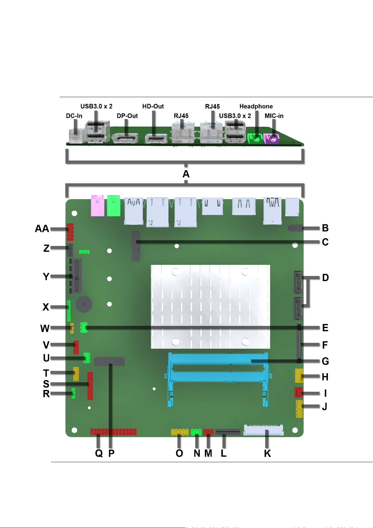
Desktop Board Components
Figure shows the approximate location of the major components on the top side of
MiTAC Desktop Board PD10AI.
Figu re : MiT A C D e s kt o p B o ar d P D1 0 AI C o m po n e nts ( T o p )
4
Page 5

A Back
P
anel
C
onnectors
B 12V 2-PIN DC
-in
C M.2 Key
-E
D SATA 7
-
Pin Connector
E Com2 RS232 Power Select
F SATA Power Connector
G SO-DIMM
slot
H CPU Fan Header
I System Fan Header
J Chassis Front I/O Header
K LVDS Connector (eDP Connector at the bottom side)
L Panel Power
M LCD Panel Power Select
N Inverter Power Select
O USB 2.0 Header
P M.2 Key
-M
Q Parallel port/ MiAPI Header
R CMOS Reset
S Legacy I/O Header
T COM1 RS232
U COM1 RS232 Power Select
V COM2 RS232
W AT/ATX Mode
X MCU Program Header
Y PCI Express X1
Connector
Z Speaker Header
AA Front Panel Audio Header
T
AB L E
: MITA C D
ES K T O P BOA R D
PD10AI C
OM P ONENTS
5
Page 6

Processor
MITAC Desktop Board PD10AI includes a passively-cooled, Intel Apollo Lake N3350/N4200
processor with integrated graphics and memory controller. The processor is soldered
to the Desktop Board and is not customer upgradeable.
NOTE
The board is designed to be passively cooled in a properly ventilated chassis. Chassis
venting locations are recommended above the processor heatsink area for maximum
heat dissipation effectiveness.
System Memory
NOTE
To be fully compliant with all applicable SDRAM memory specifications, the
board should be populated with DIMMs that support the Serial Presence Detect (SPD)
data structure. If your memory modules do not support SPD, you will see a
notification to this effect on the screen at power up. The BIOS will attempt to
configure the memory controller for normal operation.
The Desktop Board has two 204-pin DDR3L SO-DIMM sockets with gold-plated contacts.
These sockets support:
Support for DDR3L SO-DIMMs
Serial Presence Detect (SPD) memory only
Non-ECC memory
Up to 8 GB of memory (on a single SO-DIMM or 4 GB each by 2 SO-DIMM)
6
Page 7

Page 8

Page 9

Page 10

Page 11
Page 12
Page 13
Page 14
Page 15

Page 16
Page 17
Page 18
Page 19

1. GENERAL OVERVIEW
This document specifies the BIOS requirements for PD10AI
Note: The BIOS specification may be changed depend on hardware design. This is based on the product
specification document (PRD).
1.1 HARDWARE OVERVIEW
1.1.1 CPU
- Intel Apollo Lake N4200/N3350
1.1.2 System Memory
-
DDR3L 1867 Mhz (up to 8GB) 2*SODIMM Socket
1.1.3 BIOS ROM
- 64Mbit SPI Flash ROM
1.1.4 Super I/O
- Nutovon NCT6793D
1.1.5 Keyboard/Mouse
- Standard USB Devices
1.1.6 Storage
- SATA HDD
1.1.7 Graphics
- Intel HD Graphic
- 1x HDMI, 1x VGA,1xLVDS, 1xeDP
1.1.8 Audio
- Intel HD audio, Realtek ALC283 Codec co-design
1.1.9 LAN
- Intel I211-AT x2
1.1.10 Add-in Slot
- PCI Express x1 slot x1
- 1 x 2280, 2260 & 2242 M.2 (with USB, & SATA III Signal)
- 1 x 2230 M.2 (with PCIe x1 Channel & USB Signal)
1.1.11 Internal Header
- LVDS / eDP Header (Switch)
- 2 Internal SATA(Black/Fully Shrouded)
- One SATA is multiplexed with an M.2 port
Page 20

- Dual-Port USB2.0 Header
- Chassis main panel header (2x5) (Black w/multi color)
- BIOS Recovery Header/Jumper
- Audio header (front panel mic/hp) (2x5)
- Onboard Speaker header
- SATA power (15pin SATA power)
- 2 Serial Port Headers , configurable for power RS232
- Jump for AT/ATX mode
- Parallel Port Header
- MiAPI Header co-lay with optional 1x parallel port header (2x13)
- Legacy IO board header
- Fruit Tart header
1.1.12 External I/O
- 2-port USB 3.0
- RJ45x2
- DP out
- 2-port USB 3.0
- HD-out
- Mic in
- Line out
1.1.13 Supporting OS
- Windows 10 (No WHCK)
- Linux Ubuntu LTS
- Fedora, RHEL, Debian (Installation)
Page 21

1.1.14 GPIO Pin Definition
PCH
Pin
Pin Name Selected Function/Net Name
GPIO_205 / PCIE_WAKE0_N
R62
1.8V
GPIO_206 / PCIE_WAKE1_N
P62
1.8V
GPIO_207 / PCIE_WAKE2_N
P61
1.8V
GPIO_208 / PCIE_WAKE3_N
N62
1.8V
GPIO_156 / EMMC_CLK
Y58
1.8V
GPIO_157 / EMMC_D0
V58
1.8V
GPIO_158 / EMMC_D1
T58
1.8V
PCIE_WAKE0_N
PCIE_WAKE1_N
PCIE_WAKE2_N
PCIE_WAKE3_N
NC
NC
NC
/ M2E_WAKE_0_N
/ GLAN0_WAKE_1_N
/ X1_WAKE_2_N
/ GLAN1_WAKE_3_N
BIOS programming/
Comment
GPI/
PU 10K to V_1P8_A
GPI /
PU 10K to V_1P8_A
GPI /
PU 10K to V_1P8_A
GPI /
PU 10K to V_1P8_A
GPO/
NC
GPO/
NC
GPO/
NC
GPIO_159 / EMMC_D2
T59
1.8V
GPIO_160 / EMMC_D3
V51
1.8V
GPIO_161 / EMMC_D4
V52
1.8V
GPIO_162 / EMMC_D5
Y49
1.8V
GPIO_163 / EMMC_D6
V55
1.8V
GPIO_164 / EMMC_D7
V57
1.8V
GPIO_165 / EMMC_CMD
Y51
1.8V
GPIO_166 / SDIO_CLK
P58
1.8V
NC
GPO/
NC
GPO/
NC
NC
GPO/
NC
NC
GPO/
NC
NC
GPO/
NC
NC
GPO/
NC
NC
GPO/
NC
NC
GPO/
NC
NC
GPIO_167 / SDIO_DO
T52
1.8V
P57 GPIO_168 / SDIO_D1
NC
NC GPO/
GPO/
NC
Page 22

1.8V
NC
T54
T55
T57
AB58
AC49
AC48
AC51
AB51
GPIO_169 / SDIO_D2
1.8V
GPIO_170 / SDIO_D3
1.8V
GPIO_171/ SDIO_CMD
1.8V
GPIO_172 / SDCARD_CLK
1.8V
GPIO_173 / SDCARD_D0
1.8V
GPIO_174 / SDCARD_D1
1.8V
GPIO_175 / SDCARD_D2
1.8V
GPIO_176 / SDCARD_D3
1.8V
NC
GPO/
NC
GPO/
NC
NC
GPO/
NC
NC
GPO/
NC
NC
GPO/
NC
NC
GPO/
NC
NC
GPO/
NC
NC
GPO/
NC
NC
AB54
AC52
AB55
V54
P51
AR62
AR63
AN62
GPIO_177 / SDCARD_CD_N
1.8V
GPIO_178 / SDCARD_CMD
1.8V
GPIO_186 / SDCARD_LVL_WP
1.8V
GPIO_182 / EMMC_RCLK
1.8V
GPIO_183 / SDIO_PWR_DOWN_N
1.8V
GPIO_124 / LPSS_I2C0_SDA
1.8V
GPIO_125 / LPSS_I2C0_SCL
1.8V
GPIO_126 / LPSS_I2C1_SDA
1.8V
NC
GPO/
NC
GPO/
NC
NC
GPO/
NC
NC
GPO/
NC
NC
GPO/
NC
NC
GPO/
NC
NC
GPO/
NC
NC
GPO/
NC
NC
AM61
GPIO_127 / LPSS_I2C1_SCL
1.8V
GPIO_128 / LPSS_I2C2_SDA
AP59
1.8V
AP58 GPIO_129 / LPSS_I2C2_SCL
NC
GPO/
NC
GPO/
NC
NC
NC GPO/
Page 23

1.8V
NC
AM62
AL62
AP52
AP54
AP49
AP51
AL63
AK61
GPIO_130 / LPSS_I2C3_SDA
1.8V
GPIO_131 / LPSS_I2C3_SCL
1.8V
GPIO_132 / LPSS_I2C4_SDA
1.8V
GPIO_133 / LPSS_I2C4_SCL
1.8V
GPIO_134 / LPSS_I2C5_SDA
1.8V
GPIO_135 / LPSS_I2C5_SCL
1.8V
GPIO_136 / LPSS_I2C6_SDA
1.8V
GPIO_137 / LPSS_I2C6_SCL
1.8V
NC
GPO/
NC
GPO/
NC
NC
GPO/
NC
NC
GPO/
NC
NC
GPO/
NC
NC
GPO/
NC
NC
GPO/
NC
NC
GPO/
NC
NC
AP62
AP61
AM48
AK58
AK51
AM54
AM51
AM49
GPIO_138 / LPSS_I2C7_SDA
1.8V
GPIO_139 / LPSS_I2C7_SCL
1.8V
GPIO_146 / ISH_GPIO_0
1.8V
GPIO_147 / ISH_GPIO_1
1.8V
GPIO_148 / ISH_GPIO_2
1.8V
GPIO_149 / ISH_GPIO_3
1.8V
GPIO_150 / ISH_GPIO_4
1.8V
GPIO_151 / ISH_GPIO_5
1.8V
NC
NC
Fn 2: AVS_HDA_BCLK/IO
HDA_BIT_CLK
Fn 2: AVS_HDA_WS_SYNC
HDA_SYNC
Fn 2: AVS_HDA_SDI/Input
AUD_LINK_SDI0
Fn 2: AVS_HDA_SDO/Out
HDA_SDATA_OUT
NC
NC
GPO/
NC
GPO/
NC
AUD_LINK_BCLK
TO AUDIO CODE
AUD_LINK_SYNC
TO AUDIO CODE
AUD_LINK_SDI
TO AUDIO CODE
AUD_LINK_SDO
TO AUDIO CODE
GPO/
NC
GPO/
NC
AM57
GPIO_152 / ISH_GPIO_6
1.8V
GPIO_153 / ISH_GPIO_7
AM55
1.8V
AM52 GPIO_154 / ISH_GPIO_8
NC
GPO/
NC
GPO/
NC
NC
NC GPO/
Page 24

1.8V
NC
AK57
AK62
AH62
AH61
AJ62
AK49
AG55
C49
GPIO_155 / ISH_GPIO_9
1.8V
GPIO_209 / PCIE_CLKREQ0_N
1.8V
GPIO_210 / PCIE_CLKREQ1_N
1.8V
GPIO_211 / PCIE_CLKREQ2_N
1.8V
GPIO_212 / PCIE_CLKREQ3_N
1.8V
GPIO_220 / PMU_AC_PRESENT
1.8V / 3.3V
GPIO_221 / EMMC_PWR_EN_N
1.8V / 3.3V
GPIO_187 / HV_DDI0_DDC_SDA
1.8V
Fn2: SPKR
AUD_SPKR
PCIE_CLKREQ0_N/
M2E_CLKREQ_0
PCIE_CLKREQ1_N/
PU_LAN0_CLKREQ_1
PCIE_CLKREQ2_N/
PU_PCIE_X1_CLKREQ_2
PCIE_CLKREQ3_N/
PU_LAN1_CLKREQ_3
PMU_AC_PRESENT
EMMC_PWR_EN
PMU_HDMI_DATA
AUD_SPKR
TO AUDIO CODE
Native/
PU 10K to V_1P8_A
Native/
PU 10K to V_1P8_A
Native/
PU 10K to V_1P8_A
Native/
PU 10K to V_1P8_A
GPI/
PU 10K to 3VSB
GPI/
PU 10K to 3VSB
Native/
GPIO_188 / HV_DDI0_DDC_SCL
B49
1.8V
GPIO_189 / HV_DDI1_DDC_SDA
C54
1.8V
GPIO_190 / HV_DDI1_DDC_SCL
A54
1.8V
GPIO_191 / MIPI_I2C_SDA
B51
1.8V
GPIO_192 / MIPI_I2C_SCL
C51
1.8V
GPIO_193 / PNL0_VDDEN
C47
1.8V
GPIO_194 / PNL0_BKLTEN
B47
1.8V
GPIO_195 / PNL0_BKLTCTL
C46
1.8V
PMU_HDMI_CLK
DP_CTRLDATA
DP_CTRLCLK
NC
NC
NC
NC
NC
Native/
Native/
Native/
GPO/
NC
GPO/
NC
GPO/
NC
GPO/
NC
GPO/
NC
GPIO_196 / PNL1_VDDEN
B53
BRS_BKLT_EN Native/
1.8V
GPIO_197 / PNL1_BKLTEN
C53
BRS_VDD_EN Native/
1.8V
C52 GPIO_198 / PNL1_BKLTCTL
BRS_BKLT_CTRL Native/
Page 25

1.8V
GPIO_199 / HV_DDI1_HPD
A50
1.8V
GPIO_200 / HV_DDI0_HPD
C50
1.8V
GPIO_201 / MDSI_A_TE
M45
1.8V
GPIO_202 / MDSI_C_TE
M43
1.8V
GPIO_203 / USB_OC0_N
B55
1.8V
GPIO_204 / USB_OC1_N
C55
1.8V
GPIO_223
F48
1.8V
GPIO_213
M47
1.8V
Fn2: DDI1_HPD
DP_HP_DET_PCH
Fn2: DDI0_HPD
HDMI_HPD_N
NC
NC
USB_OC_0
USB_OC_1
NC
NC
Native/ Enable 20k pull up
PU 8.2K to V_1P8_A
Native/ Enable 20k pull up
PU 8.2K to V_1P8_A
GPO/
NC
GPO/
NC
Native/
Native/
GPO/
NC
GPO/
NC
GPIO_214
L47
1.8V
GPIO_215
P47
1.8V
GPIO_224
J45
1.8V
GPIO_74 / AVS_I2S1_MCLK
G62
1.8V
GPIO_75 / AVS_I2S1_BCLK
H63
1.8V
GPIO_76 / AVS_I2S1_WS_SYNC
J62
1.8V
GPIO_77 / AVS_I2S1_SDI
K61
1.8V
GPIO_78 / AVS_I2S1_SDO
K62
1.8V
NC
NC
NC
NC
NC
NC
NC
SMB_MODE_SET
GPO/
NC
GPO/
NC
GPO/
NC
GPO/
NC
GPO/
NC
GPO/
NC
GPO/
NC
GPO/ (HW strapping)
PD 10K to GND
GPIO_79 / AVS_DMIC_CLK_A1
P54
1.8V
GPIO_80 / AVS_DMIC_CLK_B1
P52
1.8V
M54 GPIO_81 / AVS_DMIC_DATA_1
NC
NC
NC GPO/
GPO/
NC
GPO/
NC
Page 26

1.8V
NC
GPIO_82 / AVS_DMIC_CLK_AB2
M55
1.8V
GPIO_83 / AVS_DMIC_DATA_2
M52
1.8V
GPIO_84 / AVS_I2S2_MCLK
K58
1.8V
GPIO_85 / AVS_I2S2_BCLK
H59
1.8V
GPIO_86 / AVS_I2S2_WS_SYNC
M57
1.8V
GPIO_87 / AVS_I2S2_SDI
K59
1.8V
GPIO_88 / AVS_I2S2_SDO
M58
1.8V
GPIO_89 / AVS_I2S3_BCLK
M62
1.8V
RSVD_GPIO_82
NC
Fn 2: AVS_HDA_RST_N
HDA_RST-
NC
NC
NC
PMU_MODE_SET
NC
GPO/ (HW strapping)
PD 10K to GND
GPO/
NC
AVS_HDA_RST_N/
TO AUDIO CODE
GPO/
NC
GPO/
NC
GPO/
NC
GPO/ (HW strapping)
PD 10K to GND
GPO/
NC
GPIO_90 / AVS_I2S3_WS_SYNC
M61
1.8V
GPIO_91 / AVS_I2S3_SDI
L62
1.8V
GPIO_92 / AVS_I2S3_SDO
L63
1.8V
GPIO_97 / FST_SPI_CS0_B
B57
1.8V
GPIO_98 / FST_SPI_CS1_B
C57
1.8V
GPIO_99 / FST_SPI_MOSI_IO0
A58
1.8V
GPIO_100 / FST_SPI_MOSI_IO1
B58
1.8V
GPIO_101 / FST_SPI_IO2
B60
1.8V
NC
NC
SMB_REBOOT
SPI_CS_N
NC NC
SPI_MOSI
SPI_MISO
NC Native/
GPO/
NC
GPO/
NC
GPO/ (HW strapping)
PD 10K to GND
Native/
Native/
Native/
GPIO_102 / FST_SPI_IO3
B61
NC Native/
1.8V
GPIO_103 / FST_SPI_CLK
Native/
C56
SPI_CLK
1.8V
F54 GPIO_104 / FST_SPI_0_CLK
RSVD_GPIO_104
GPO/ (HW strapping)
Page 27

1.8V
PD 10K to GND
GPIO_105 / FST_SPI_0_FS0
F52
1.8V
GPIO_106 / FST_SPI_0_FS1
H52
1.8V
GPIO_109 / FST_SPI_0_RXD
H54
1.8V
GPIO_110 / FST_SPI_0_TXD
J52
1.8V
GPIO_111 / SIO_SPI_1_CLK
F58
1.8V
GPIO_112 / SIO_SPI_1_FS0
K55
1.8V
GPIO_113 / SIO_SPI_1_FS1
F61
1.8V
GPIO_116 / SIO_SPI_1_RXD
H57
1.8V
RSVD_GPIO_105
RSVD_GPIO_106
NC NC
LPC_MODE_SET
SPI_BOOT_GPIO111
RSVD_GPIO_112
RSVD_GPIO_113
NC NC
GPO/ (HW strapping)
PD 10K to GND
GPO/ (HW strapping)
PU 10K to V_1P8_A
GPO/ (HW strapping)
PD 10K to GND
GPO/ (HW strapping)
PD 10K to GND
GPO/ (HW strapping)
PD 10K to GND
GPO/ (HW strapping)
PD 10K to GND
GPIO_117 / SIO_SPI_1_TXD
H58
1.8V
GPIO_118 / SIO_SPI_2_CLK
F62
1.8V
GPIO_119 / SIO_SPI_2_FS0
D61
1.8V
GPIO_120 / SIO_SPI_2_FS1
E56
1.8V
GPIO_121 / SIO_SPI_2_FS2
D59
1.8V
GPIO_122 / SIO_SPI_2_RXD
C62
1.8V
GPIO_123 / SIO_SPI_2_TXD
E62
1.8V
GPIO_0
A38
1.8V
RSVD_GPIO_117
SPI_OVERRIDE
NC NC
TOP_SWAP_OVERRIDE
RSVD_GPIO_121
NC NC
RSVD_GPIO_123
NC
GPO/ (HW strapping)
PD 10K to GND
GPO/ (HW strapping)
PD 10K to GND
GPO/ (HW strapping)
PD 10K to GND
GPO/ (HW strapping)
PD 10K to GND
GPO/ (HW strapping)
PU 10K to V_1P8_A
GPO/
NC
GPIO_1
B33
1.8V
GPIO_2
C39
1.8V
B39 GPIO_3
NC
NC
NC GPO/
GPO/
NC
GPO/
NC
Page 28
1.8V
NC
B35
A34
B31
H39
B29
A30
L39
C34
GPIO_4
1.8V
GPIO_5
1.8V
GPIO_6
1.8V
GPIO_7
1.8V
GPIO_8
1.8V
GPIO_9
1.8V
GPIO_10
1.8V
GPIO_11
1.8V
NC
GPO/
NC
GPO/
NC
NC
GPO/
NC
NC
GPO/
SOC_TPM_ENABLE_N
PU 10K to V_1P8_A
GPO/
MUX_SEL_EN_PMC
PU 10K to V_1P8_A
GPI/
DISPLAY_RESET_N
PU 10K to V_1P8_A
GPO/
INT_SPK_SD_N
PU 10K to V_1P8_A
GPI/
BRIGHTNESS_DOWN_PMC
PU 10K to V_1P8_A
E39
C30
C38
F39
C36
C35
J39
C33
GPIO_12
1.8V
GPIO_13
1.8V
GPIO_14
1.8V
GPIO_15
1.8V
GPIO_16
1.8V
GPIO_17
1.8V
GPIO_18
1.8V
GPIO_19
1.8V
BRIGHTNESS_UP_PMC
1P8_PWRBT_N
WLAN_DISABLE_0_N_PMC
WLAN_DISABLE_1_N_PMC
EDID_ISO_N_PMC
PS8625_PD_N_PMC
CODEC_DISABLE_N_PMC
LAN1_DISABLE_N
GPI/
PU 10K to V_1P8_A
GPI/
PU 10K to V_1P8_A
GPO/
PU 10K to V_1P8_A
GPO/
PU 10K to V_1P8_A
GPO/
PU 10K to V_1P8_A
GPO/
PU 10K to V_1P8_A
GPO/
PU 10K to V_1P8_A
GPO/
PU 10K to V_1P8_A
GPIO_20
B27
1.8V
GPIO_21
C26
1.8V
A26 GPIO_22
NC
HDMID_CEC
F_AUDIO_DET_N_PMC GPI/
GPO/
NC
GPI/
PU 10K to V_1P8_A
Page 29

1.8V
PU 10K to V_1P8_A
B25
C25
C27
C31
C29
B37
H35
C37
GPIO_23
1.8V
GPIO_24
1.8V
GPIO_25
1.8V
GPIO_26
1.8V
GPIO_27
1.8V
GPIO_28
1.8V
GPIO_29
1.8V
GPIO_30
1.8V
MSATA_DET_N
PMU_PME_N
Fn 5: SATA_DEVSLP1
DEVLSP1
Fn 5: SATA_LEDN
SATA_LED_N
LAN0_DISABLE_N
NC
NC
NC
GPI/
PU 10K to V_1P8_A
GPI/
PU 10K to V_1P8_A
SATA_DEVSLP1
TO M.2 Key B Slot
SATA_LEDN
GPO/
PU 10K to V_1P8_A
GPO/
NC
GPO/
NC
GPO/
NC
GPIO_31
H34
1.8V
GPIO_32
F35
1.8V
GPIO_33
F34
1.8V
GPIO_34/PWM0
B41
1.8V
GPIO_35/PWM1
C41
1.8V
GPIO_36/PWM2
F41
1.8V
GPIO_36/PWM3
E41
1.8V
GPIO_38 / LPSS_UART0_RXD
C45
1.8V
NC
NC
NC
RSVD_GPIO_34
RSVD_GPIO_35
RSVD_GPIO_36
NC
NC
GPO/
NC
GPO/
NC
GPO/
NC
GPO/ (HW strapping)
PD 10K to GND
GPO/ (HW strapping)
PD 10K to GND
GPO/ (HW strapping)
PD 10K to GND
GPO/
NC
GPO/
NC
GPIO_39 / LPSS_UART0_TXD
B45
1.8V
GPIO_40 / LPSS_UART0_RTS_N
A46
1.8V
C44 GPIO_41 / LPSS_UART0_CTS_N
CSE_EN
RTC_BYPASS
NC GPO/
GPO/ (HW strapping)
PD 10K to GND
GPO/ (HW strapping)
PD 10K to GND
Page 30

1.8V
NC
GPIO_42 / LPSS_UART1_RXD
C43
1.8V
GPIO_43 / LPSS_UART1_TXD
B43
1.8V
GPIO_44 / LPSS_UART1_RTS_N
A42
1.8V
GPIO_45 / LPSS_UART1_CTS_N
C42
1.8V
GPIO_46 / LPSS_UART2_RXD
J41
1.8V
GPIO_47 / LPSS_UART2_TXD
H41
1.8V
GPIO_48 / LPSS_UART2_RTS_N
L41
1.8V
GPIO_49 / LPSS_UART2_CTS_N
M41
1.8V
NC
RSVD_GPIO_43
BOOT_SPI_SET
NC
NC
CSE_FW_SET
RSVD_GPIO_48
NC
GPO/
NC
GPO/ (HW strapping)
PD 10K to GND
GPO/ (HW strapping)
PU 10K to V_1P8_A
GPO/
NC
GPO/
NC
GPO/ (HW strapping)
PD 10K to GND
GPO/ (HW strapping)
PD 10K to GND
GPO/
NC
GPIO_62 / GP_CAMERASB00
L37
1.8V
GPIO_63 / GP_CAMERASB01
P34
1.8V
GPIO_64 / GP_CAMERASB02
J34
1.8V
GPIO_65 / GP_CAMERASB03
H30
1.8V
GPIO_66 / GP_CAMERASB04
M37
1.8V
GPIO_67 / GP_CAMERASB05
F30
1.8V
GPIO_68 / GP_CAMERASB06
R35
1.8V
GPIO_69 / GP_CAMERASB07
L34
1.8V
NC
GPO/
NC
GPO/
NC
NC
GPO/
NC
NC
GPO/
NC
NC
GPO/
NC
NC
GPO/
NC
NC
GPO/
NC
NC
GPO/
NC
NC
GPIO_70 / GP_CAMERASB08
M34
1.8V
GPIO_71 / GP_CAMERASB09
M35
1.8V
R34 GPIO_72 / GP_CAMERASB10
NC
NC
NC GPO/
GPO/
NC
GPO/
NC
Page 31

1.8V
NC
GPIO_73 / GP_CAMERASB11
E30
1.8V
GPIO_216
P30
1.8V
GPIO_217
M29
1.8V
GPIO_218
M30
1.8V
GPIO_219 / EMMC_RST_N
L30
1.8V
NC
GPO/
NC
GPI/
LEGACY_IO_DET_N_R
PU 10K to V_1P8_A
GPI/
BOARD_ID_0
PU 10K to V_1P8_A
GPI/
BOARD_ID_1
PU 10K to V_1P8_A
NC NC
Page 32

1.2 REFERENCES
CPU Specification :
557555_APL_EDS_1p5_Volume_1.pdf
557556_EDS_Volume_2_Revision_0p7.pdf
557557_EDS_Volume_3_Revison_0p7.pdf
559360_Volume_4_EDS_0p7_Unstructured_Final.pdf
Trusted Execution Engine Specification
562802_APL_BXT_TXEFWCompGuide_Rev0p85.pdf
:
Super I/O Specification :
NCT6793D_Datasheet_V1_0.pdf
Others :
559810_APL_BXT_IAFW_Vol1_BIOSSpec_Rev_0p7p1.pdf
559811_APL_BXT_IAFW_Vol2_BIOSSpec_Rev_0p7p1.pdf
561027_APL_RMT_UG_Rev0p6.pdf
Page 33

2. BIOS OVERVIEW
AMI APTIO Core 5.011
Code Base : 1ATJS010
Support Platform : Intel Apollo Lake
Support Intel GOP VBIOS : 10.0.1027(64bit)
Provide BIOS Setup Utility
Support Advanced Configuration and Power Interface (ACPI 2.0 or later)
Support DMI 2.3.1 or later
Support BIOS Boot Specification 1.01 or higher
Support Plug and Play 1.0a, PCI Express 1.0a
Support USB 1.1 / 2.0 / 3.0
Support USB wake up from S3
Support Advanced Hard disk Features (Not support HDD security)
Support USB legacy (Keyboard & Mouse & Floppy & CD-ROM)
Support Wake on LAN (DeepSleep must disabled.)
Support Boot Control Features (Boot devices sequence selections)
Support Security password: BIOS Setup Administrator password only
Support OEM Activation 3.0
Support UEFI PXE Boot IPv4/IPv6.
Support RTC wake up from S3/S4/S5
Support FAN Control
Page 34
3. POST
3.1 OVERVIEW
When a computer is turned on, the BIOS runs a Power-On Self Test (POST). Program execution
start at memory location F000:FFF0h. This address is part of ROM BIOS and contains a jump
command to a series of BIOS routines that test and initialize the hardware components. POST
consists of various test and initialization routines for chipset’ processor and hardware
components. When all test have been performed and components have been initialized, control
is transferred to the INT 19h Bootstrap Loader, to load the available operating system on the disk.
During the POST period, a value form 00h through FFh is written to the manufacturing test port
(generally is I/O port 80h). These values are known as POST Diagnostic Codes. (refer to
appendix in detail)
3.2 SPLASH SCREEN
POST Logo: N/A
3.3 HOT KEY OPTIONS
Hot keys should be accepted during POST. The following Hot Keys are required at boot time.
<F2> or <DEL> to Enter BIOS setup utility.
F7 =>Popup boot menu. The user will be presented with a list of boot options that they may select a
device to boot from (i.e., override the existing boot list for that particular boot).
3.4 BIOS WARNING EVENT LIST
Event Warning Message
POST Memory not detect Three long beep code
4. BIOS SETUP UTILITY
During POST, the end user can press<F2> <DEL> to enter Setup and change the system parameters
originally specified in the BIOS defaults. The Setup items are described in BIOS Setup Specification.
BIOS Setup Specification for detail.
Page 35
5. POWER MANAGEMENT
5.1 ACPI (ADVANCED CONFIGURATION AND POWER INTERFACE)
5.1.1 Overview
ACPI 2.0 or later compatibility.
System support Full on state (S0), Suspend to RAM (STR - S3), Hibernation/Suspend to Disk (STD - S4),
Soft Off (S5)
5.1.2 System Power States and Wakeup Event Resource
S3 S4 S5 DeepSleep Enabled in S4-S5
USB Keyboard/Mouse Yes No No No
RTC Yes Yes Yes No
Wake on LAN (WOL) Yes Yes Yes No
Power Button Yes Yes Yes Yes
5.1.3 Power Button
In ACPI mode, Power Button switches the system from the sleeping/soft off state to the working state,
and signals the OS to transition to a sleeping state from the working state. In NON ACPI mode, Power
button is only to turn on/off system.
6. SUBSYSTEM ID OVERVIEW
The purpose of Subsystem Vendor ID and the Subsystem Device ID is further identifying the PCI device.
The Subsystem Vendor ID is that of the board/card manufacturer. The Subsystem Device ID is assigned
by the subsystem vendor.
For on-brand board/system, BIOS needs to configure MiTAC SVID as manufacturer ID (to identify for
DTM verification) & SSID (used project code).
Name
SVID
SSID
Value (Hex)
1071
0767
Page 36

7. /SMBIOS OVERVIEW
Desktop Management Interface (DMI) / System Management BIOS (SMBIOS) is a method of managing
computers in an enterprise. The main component of DMI/SMBIOS is the Management Information Format
Database. This database contains all the information about the computing system and its components.
Using DMI/SMBIOS, a system administrator can obtain the types, capabilities, operational status,
installation date, and other information about the system components.
[System Information] (Type 1)
Manufacturer (String1) - "MiTAC"
Product Name (String2) - "PD10AI"
Version (String3) - " "
Serial Number (String4) - " "
UUID: 0x00 0x02 0x00 0x03 0x00 0x04 0x00 0x05 0x00 0x06 0x00 0x07 0x00 0x08 0x00 0x09
Wakeup Type: 0x06 - Power Switch
SKU Number (String5) - " "
[Base Board Information] (Type 2)
Manufacturer (String1) - "MiTAC"
Product (String2) - "PD10AI"
Version (String3) - " "
Serial Number (String4) - " "
Asset Tag (String5) - " "
Board Type: 0x0A - Motherboard (includes processor, memory, and I/O)
[System Enclosure or Chassis] (Type 3)
Manufacturer (String1) - "MiTAC"
Enclosure Type: 0x03 - Desktop
Version (String2) - " "
Serial Number (String3) - " "
Asset Tag Number (String4) - " "
Boot-up State: 0x03 - Safe
Power Supply State: 0x03 - Safe
Thermal State: 0x03 - Safe
Security State: 0x03 - None
OEM-defined: 0x00000000
Page 37
Height: 0x00 (0)
Number of Power Cords: 0x01 (1)
Contained Element Count: 0x00 (0)
Element Record Length: 0x00 (0)
SKU Number (String5) - " "
8. UTILITIES
8.1 BIOS FLASH
If BIOS supports multi BIOS ROM, the flash utility should support them.
Vender Name Model Name
Winbond W25Q128FW
MXIC MX25U12873F
Page 38

9. BIOS RELEASE
9.1 BIOS REVISION
MiTAC BIOS Naming:
D767 0 A 01
SKU B/C 1 2 3
1: Sku ID; “0” for MiTAC
2: Stage;
X =>Develop Stage.
T =>Test Stage.
A =>Production Stage
3: Version number (Decimal);
9.2 RELEASE COMPONENT
Release BIOS ROM and Flash Utility for each BIOS release. If Flash Utility is not modified, may not
release Flash Tool. Enforce the virus check of the release component.
Send Release Note for each BIOS release.
Release Note contains added features, fixed issues & known restriction.
9.3 BIOS RELEASE
FTP Server
PLM
EMAIL
9.4 DISTRIBUTION LIST FOR BIOS RELEASE
Customer, RD, CAD, QA.
9.5 BIOS RELEASE NOTE FORMAT
//********************************************************************************
// Revision No. :
// Build Date :
// ME Version :
// GbE PHY :
// GbE Option Rom Version :
// VBIOS Version :
// GOP Driver Version :
Page 39

// Checksum :
// ValleyView MRC Version :
//********************************************************************************
// MicroCode revision & CPU Support List :
//M0230671116 ("Intel(R) ValleyView A-0 Stepping")
//M0230672219 ("Intel(R) ValleyView B-1 Stepping")
//M0C3067330C("Intel(R) ValleyView B-2 Stepping")
//********************************************************************************
// Reference Code revision :
// ValleyView: reference code ver.
// NorthBridge ValleyView - SystemAgent: reference code ver.
// SouthBridge ValleyView: reference code label ver.
// ValleyView PowerManagement PPM Intel Reference code ver.
// ValleyView ACPI Reference code ver.
// Manageability Engine (ME) reference code ver.
// Fast Flash Standby (FFS) reference code ver.
//********************************************************************************
Release History:
10. QUALITY
10.1 MAINTENANCE
Support new function and new OS in nearly future as many as possible
Support simple changing from our customer’s BIOS requests.
For example,
- Change the default value in BIOS Setup
- Change the boot device order in BIOS Setup.
Page 40

10.2 BIOS QA TEST
Must to PASS below tests before release
BIOS version (correct version)
BIOS Setup (including "Restore Defaults", "Discard Changes" and clear CMOS) (follow spec)
S3/S4/S5 power cycling tests over 100 times (without any error)
Hot Keys (function normal)
Windows Device manager (no “!”)
BIOS Flash (successful & check correct BIOS version, Setup without changes & no “!” in Windows device
manager)
Fixed Bugs (verified okay)
Regression tests
11. APPENDIX
POST Diagnostic Codes
Status Code Ranges
Status Code Range Description
0x01 – 0x0F SEC Status Codes & Errors
0x10 – 0x2F PEI execution up to and including memory detection
0x30 – 0x4F PEI execution after memory detection
0x50 – 0x5F PEI errors
0x60 – 0xCF DXE execution up to BDS
0xD0 – 0xDF DXE errors
0xE0 – 0xE8 S3 Resume (PEI)
0xE9 – 0xEF S3 Resume errors (PEI)
0xF0 – 0xF8 Recovery (PEI)
0xF9 – 0xFF Recovery errors (PEI)
Page 41

Standard Status Codes
SEC Status Codes
Status Code Description
0x0 Not used
Progress Codes
0x1 Power on. Reset type detection (soft/hard).
0x2 AP initialization before microcode loading
0x3 North Bridge initialization before microcode loading
0x4 South Bridge initialization before microcode loading
0x5 OEM initialization before microcode loading
0x6 Microcode loading
0x7 AP initialization after microcode loading
0x8 North Bridge initialization after microcode loading
0x9 South Bridge initialization after microcode loading
0xA OEM initialization after microcode loading
0xB Cache initialization
SEC Error Codes
0xC – 0xD Reserved for future AMI SEC error codes
0xE Microcode not found
0xF Microcode not loaded
SEC Beep Codes
None
PEI Status Codes
Status Code Description
Progress Codes
0x10 PEI Core is started
0x11 Pre-memory CPU initialization is started
0x12 Pre-memory CPU initialization (CPU module specific)
0x13 Pre-memory CPU initialization (CPU module specific)
0x14 Pre-memory CPU initialization (CPU module specific)
0x15 Pre-memory North Bridge initialization is started
0x16 Pre-Memory North Bridge initialization (North Bridge module specific)
0x17 Pre-Memory North Bridge initialization (North Bridge module specific)
0x18 Pre-Memory North Bridge initialization (North Bridge module specific)
0x19 Pre-memory South Bridge initialization is started
Page 42

0x1A Pre-memory South Bridge initialization (South Bridge module specific)
0x1B Pre-memory South Bridge initialization (South Bridge module specific)
0x1C Pre-memory South Bridge initialization (South Bridge module specific)
0x1D – 0x2A OEM pre-memory initialization codes
0x2B Memory initialization. Serial Presence Detect (SPD) data reading
0x2C Memory initialization. Memory presence detection
0x2D Memory initialization. Programming memory timing information
0x2E Memory initialization. Configuring memory
0x2F Memory initialization (other).
0x30 Reserved for ASL (see ASL Status Codes section below)
0x31 Memory Installed
0x32 CPU post-memory initialization is started
0x33 CPU post-memory initialization. Cache initialization
0x34 CPU post-memory initialization. Application Processor(s) (AP) initialization
0x35 CPU post-memory initialization. Boot Strap Processor (BSP) selection
0x36 CPU post-memory initialization. System Management Mode (SMM) initialization
0x37 Post-Memory North Bridge initialization is started
0x38 Post-Memory North Bridge initialization (North Bridge module specific)
0x39 Post-Memory North Bridge initialization (North Bridge module specific)
0x3A Post-Memory North Bridge initialization (North Bridge module specific)
0x3B Post-Memory South Bridge initialization is started
0x3C Post-Memory South Bridge initialization (South Bridge module specific)
0x3D Post-Memory South Bridge initialization (South Bridge module specific)
0x3E Post-Memory South Bridge initialization (South Bridge module specific)
0x3F-0x4E OEM post memory initialization codes
0x4F DXE IPL is started
PEI Error Codes
0x50 Memory initialization error. Invalid memory type or incompatible memory speed
0x51 Memory initialization error. SPD reading has failed
0x52 Memory initialization error. Invalid memory size or memory modules do not match.
0x53 Memory initialization error. No usable memory detected
0x54 Unspecified memory initialization error.
0x55 Memory not installed
0x56 Invalid CPU type or Speed
0x57 CPU mismatch
0x58 CPU self test failed or possible CPU cache error
0x59 CPU micro-code is not found or micro-code update is failed
Page 43

0x5A Internal CPU error
0x5B reset PPI is not available
0x5C-0x5F Reserved for future AMI error codes
S3 Resume Progress Codes
0xE0 S3 Resume is stared (S3 Resume PPI is called by the DXE IPL)
0xE1 S3 Boot Script execution
0xE2 Video repost
0xE3 OS S3 wake vector call
0xE4-0xE7 Reserved for future AMI progress codes
0xE0 S3 Resume is stared (S3 Resume PPI is called by the DXE IPL)
S3 Resume Error Codes
0xE8 S3 Resume Failed in PEI
0xE9 S3 Resume PPI not Found
0xEA S3 Resume Boot Script Error
0xEB S3 OS Wake Error
0xEC-0xEF Reserved for future AMI error codes
Recovery Progress Codes
0xF0 Recovery condition triggered by firmware (Auto recovery)
0xF1 Recovery condition triggered by user (Forced recovery)
0xF2 Recovery process started
0xF3 Recovery firmware image is found
0xF4 Recovery firmware image is loaded
0xF5-0xF7 Reserved for future AMI progress codes
Recovery Error Codes
0xF8 Recovery PPI is not available
0xF9 Recovery capsule is not found
0xFA Invalid recovery capsule
0xFB – 0xFF Reserved for future AMI error codes
PEI Beep Codes
Status Code Description
0x53 Three long beep - Memory initialization error. No usable memory detected
DXE Status Codes
Status Code Description
0x60 DXE Core is started
0x61 NVRAM initialization
0x62 Installations of the South Bridge Runtime Services
Page 44

0x63 CPU DXE initialization is started
0x64 CPU DXE initialization (CPU module specific)
0x65 CPU DXE initialization (CPU module specific)
0x66 CPU DXE initialization (CPU module specific)
0x67 CPU DXE initialization (CPU module specific)
0x68 PCI host bridge initialization
0x69 North Bridge DXE initialization is started
0x6A North Bridge DXE SMM initialization is started
0x6B North Bridge DXE initialization (North Bridge module specific)
0x6C North Bridge DXE initialization (North Bridge module specific)
0x6D North Bridge DXE initialization (North Bridge module specific)
0x6E North Bridge DXE initialization (North Bridge module specific)
0x6F North Bridge DXE initialization (North Bridge module specific)
0x70 South Bridge DXE initialization is started
0x71 South Bridge DXE SMM initialization is started
0x72 South Bridge devices initialization
0x73 South Bridge DXE Initialization (South Bridge module specific)
0x74 South Bridge DXE Initialization (South Bridge module specific)
0x75 South Bridge DXE Initialization (South Bridge module specific)
0x76 South Bridge DXE Initialization (South Bridge module specific)
0x77 South Bridge DXE Initialization (South Bridge module specific)
0x78 ACPI module initialization
0x79 CSM initialization
0x7A – 0x7F Reserved for future AMI DXE codes
0x80 – 0x8F OEM DXE initialization codes
0x90 Boot Device Selection (BDS) phase is started
0x91 Driver connecting is started
0x92 PCI Bus initialization is started
0x93 PCI Bus Hot Plug Controller Initialization
0x94 PCI Bus Enumeration
0x95 PCI Bus Request Resources
0x96 PCI Bus Assign Resources
0x97 Console Output devices connect
0x98 Console input devices connect
0x99 Super IO Initialization
0x9A USB initialization is started
0x9B USB Reset
0x9C USB Detect
Page 45

0x9D USB Enable
0x9E – 0x9F Reserved for future AMI codes
0xA0 IDE initialization is started
0xA1 IDE Reset
0xA2 IDE Detect
0xA3 IDE Enable
0xA4 SCSI initialization is started
0xA5 SCSI Reset
0xA6 SCSI Detect
0xA7 SCSI Enable
0xA8 Setup Verifying Password
0xA9 Start of Setup
0xAA Reserved for ASL (see ASL Status Codes section below)
0xAB Setup Input Wait
0xAC Reserved for ASL (see ASL Status Codes section below)
0xAD Ready To Boot event
0xAE Legacy Boot event
0xAF Exit Boot Services event
0xB0 Runtime Set Virtual Address MAP Begin
0xB1 Runtime Set Virtual Address MAP End
0xB2 Legacy Option ROM Initialization
0xB3 System Reset
0xB4 USB hot plug
0xB5 PCI bus hot plug
0xB6 Clean-up of NVRAM
0xB7 Configuration Reset (reset of NVRAM settings)
0xB8 – 0xBF Reserved for future AMI codes
0xC0 – 0xCF OEM BDS initialization codes
DXE Error Codes
Status Code Description
0xD0 CPU initialization error
0xD1 North Bridge initialization error
0xD2 South Bridge initialization error
0xD3 Some of the Architectural Protocols are not available
0xD4 PCI resource allocation error. Out of Resources
0xD5 No Space for Legacy Option ROM
0xD6 No Console Output Devices are found
Page 46

0xD7 No Console Input Devices are found
0xD8 Invalid password
0xD9 Error loading Boot Option (LoadImage returned error)
0xDA Boot Option is failed (StartImage returned error)
0xDB Flash update is failed
0xDC Reset protocol is not available
DXE Beep Codes
None
ASL Status Codes
Status Code Description
0x01 System is entering S1 sleep state
0x02 System is entering S2 sleep state
0x03 System is entering S3 sleep state
0x04 System is entering S4 sleep state
0x05 System is entering S5 sleep state
0x10 System is waking up from the S1 sleep state
0x20 System is waking up from the S2 sleep state
0x30 System is waking up from the S3 sleep state
0x40 System is waking up from the S4 sleep state
0xAC System has transitioned into ACPI mode. Interrupt controller is in PIC mode.
0xAA System has transitioned into ACPI mode. Interrupt controller is in APIC mode.
OEM-Reserved Status Code Ranges
Status Code Description
0x5 OEM SEC initialization before microcode loading
0xA OEM SEC initialization after microcode loading
0x1D – 0x2A OEM pre-memory initialization codes
0x3F – 0x4E OEM PEI post memory initialization codes
0x80 – 0x8F OEM DXE initialization codes
0xC0 – 0xCF OEM BDS initialization codes
 Loading...