

Page 1
7321
7321
7321 7321
7321
7321
7321 7321
Page 2

Contents
Contents
7321 N/B Maintenance7321 N/B Maintenance
1. Hardware Engineering Specification
1.1 Introduction
1.2 System Hardware Parts
1.3 Other Functions
1.4 Peripheral Components
1.5 Software Overview
1.6 Bios Function Description
1.7 Driver / Utility Description
2. System View and Disassembly
2.1 System View
2.2 System Disassembly
3. Definition & Location Of Connectors /switches
3.1 Mother Board-a
3.2 Mother Board-b
3.3 Daughter Board
4
4
6
32
37
45
46
50
51
51
54
75
75
76
77
3.4 Charge Board
4. Definition & Location Of Major Components
78
79
1
Page 3

Contents
Contents
7321 N/B Maintenance7321 N/B Maintenance
4.1 Main Board(Side a)
4.2 Main Board(Side b)
5. Pin Description of Major Component
5.1 Mobil AMD K7 Processor
5.2 VIA VT8362 North Bridge with S3 Savage4 AGPX4
5.3 VIA VT8231 BGA PCI-LPC/ISA South Bridge
5.4 PC Card Interface controller
6. System Block Diagram
7. Maintenance Diagnostics
7.1 Introduction
7.2 Error Codes
7.3 Debug Tool
8. Trouble Shooting
8.1 No Power
8.2 Battery Can not Be Charged
79
80
81
81
84
87
97
104
105
105
106
108
110
111
114
8.3 No Display
8.4 LCD No Display or Picture Abnormal
116
118
2
Page 4

Contents
Contents
7321 N/B Maintenance7321 N/B Maintenance
8.5 External Monitor No Display or Color Abnormal
8.6 Memory Test Error
8.7 Keyboard and Touch-Pad Test Error
8.8 Hard Drive Test Error
8.9 CD-ROM Driver Test Error
8.10 Diskette Drive Test Error
8.11 USB Port Test Error
8.12 PIO Port Test Error
8.13 SIO Port Test Error
8.14 PC Card Socket Test Error
8.15 LAN Test Error
8.16 Audio Driver Error
8.17 TV Out Test Error
9. Spare Parts List
10. Circuit Diagram
121
123
125
127
129
131
133
135
137
139
141
143
146
148
158
11. Reference Material
190
3
Page 5

7321 N/B Maintenance7321 N/B Maintenance
1.Hardware Engineering Specification
1.1 Introduction
The 7321 model motherboard would support the AMD K7 processor with CPGA packaged,socket
A,which will supports the different levels of AMD K7 CPU with CPGA package,Including Athlon
650/700/750/800/900/1000 MHz,and Duron 600/650/700/750/800/900 MHz.
This system is based on PCI architecture which have standard hardware peripheral interface. The
power management complies with Advanced Configuration and Power Interface (ACPI) 1.0. It also
provides easy configuration through CMOS setup, which is built in system BIOS software and can be
pop-up by pressing F2 at system start up or warm reset. System also provides icon LEDs to display
system status, such as Power indicator, LAN, HDD/CDROM, NUM LOCK,CAP LOCK, SCROLL
LOCK, SUSPEND MODE and Battery charging status. It also equipped with Zoom Video capture port,
FIR, 2 USB ports.
The memory subsystem supports 64MB SDRAM on board and one 144 pin SO-DIMM socket for
upgrading up to maximum 320MB of DRAM using PC-100 or PC-133 SDRAM SO-DIMM module.
4
Page 6

7321 N/B Maintenance7321 N/B Maintenance
The TwisterK integrates VIA’s VT8362 KN133 system controller,S3’s Savage4 2D/3D graphics
accelerator and S3’s flat panel interfaces into a single 552 BGA package. The TwisterK SMA system
controller provides superior performance between the CPU,DRAM and PCI bus with, pipelined,burst
and concurrent operation.
Savage4 graphic accelerator integrated in TwisterK brings mainstream graphics performance with
leading-edge 2D,3D and DVD video acceleration .Also with a new super-pipelined 128-bit engine for
utilizing a single cycle architecture that provides high performance along with superior image
quality.Several new features enhance the 3D architectu re,including single-pass multitex turing, full scen e
anti-aliasing,anisotropic filtering,and an 8-bit stencil buffer.It also offers the industry’s only simultaneous
usage of single-pass multitexturing and single-cycle trilinear filtering – enabling stunning image quality
without performance loss.
The 352-pin VT8231 BGA PCI-LPC bridge supports four levels(doublewords) of line buffers,type
F DMA transfers and delay transaction to allow efficient PCI bus utilization and (PCI-2.2 compliant)
The VT8231 also includes an integrated Super I/O,integrated DS12885 style real time clock with
extended 256 byte CMOS RAM,integrated master mode enhanced IDE controller with full scatter/gather
capability and extension to UltraDMA-33/66/100 for 33/66/100 MB/sec transfer rate,integrated four
5
Page 7

7321 N/B Maintenance7321 N/B Maintenance
capability and extension to UltraDMA-33/66/100 for 33/66/100 MB/sec transfer rate,integrated four USB
interface with root hub and two function ports with built-in physical layer transceivers,Distributed DMA
support, integrated AC-97 link for basic audio and HSP based modem functions,integrated hardware
monitoring and On Now / ACPI compliant advanced configuration and power management interface.The
VT8231 also has an integrated MAC and 10Mbit PHY for LAN connection.It can bypass the internal
PHY with external home PNA with a 1Mbit PHY or a
A full set of software drivers and utilities are available to allow advanced operating systems such as
Windows 98/millennium to take full advantage of the hardware capabilities such as bus mastering IDE,
Windows 95-ready Plug & Play, Advanced Power Management (APM) and Advance configuration and
power interface (ACPI)
1.2 System Hardware Parts
Central Processing Unit
AMD K7 microprocessors in CPGA package
System frequency synthesizer
ICS9248-193
10/100Mbit PHY through the MII interface.
6
Page 8

7321 N/B Maintenance7321 N/B Maintenance
Core Logic
VIA KN133+VT8231:CPU/PCI and CPU/AGP bridge with memory/AGP/LAN/IDE/USB/PMU
and Super I/O controller
LAN—PHY
ICS1893
PC Card Interface Controller
EnE CB-1420
Dual–Slot PC Card Power Interface Switch
EnE CP-2216
AC’97 AUDIO SYSTEM
CRYSTAL CS 4299
1394
NEC uPD72872
IR MODULE
HP HSDL-3600#007
Keyboard System
HITACH H8(3434) Universal Keyboard Controller
7
Page 9

7321 N/B Maintenance7321 N/B Maintenance
System Flash Memory(BIOS)
Memory System(PC-133 compliance)
1.2.1 CPU_AMD K7(Athlon / Duron) Processor
The industry’s first nine-issue,superpiplined,superscalar x86 processor micro architecture designed
for high clock frequencies
Multiple x86 instruction decoders
Fully pipelined floating-point execution unit which executes all x87(floating point),MMX and
3Dnow! instructions
Three out-of-order,superscalar,pipelined address calculation units
Three out-of-order,superscalar,pipelined integer units
72-entry instruction control unit
Advanced dynamic branch prediction
Enhanced 3Dnow! technology with new instructions to enable improved integer math calculations
for speech or video encoding and improved data movement for internet plug-ins and other streaming
applications
200-MHz AMD Athlon System Bus (scalable beyond 400 MHz) enabling leading-edge system
bandwidth for data movement-intensive applications
High-performance cache architecture featuring an integrated 128Kbytes L1(both Athlon and Duron)
cache and a 256Kbytes (64Kbytes for Duron) L2 cache
8
Page 10

7321 N/B Maintenance7321 N/B Maintenance
1.2.2 System frequency synthesizer_ICS9248-193
1 – Differential pair open drain CPU clocks
1 – CPU clock @ 3.3V
7 – SDRAM @ 3.3V
8 – PCI @ 3.3V
1 – 48MHz @ 3.3V fixed
1 – 24/48MHz @ 3.3V
3 – REF @ 3.3V, 14.318MHz
Up to 166MHz frequency support
Support power management via hardware select CPU stop, PCI stop, and SDRAM stop
Support power management via I2C programming
Spread spectrum for EMI control (±0.2 5% t o ±0.06% center, or 0 to –0.5% or –1.0% down spread)
Uses external 14.318MHz crystal
CPU – CPU Skew: <175ps
CPU – SDRAM Skew: ±125ps
CPU – PCI Skew: ±100ps
PCI – PCI Skew: <500ps
9
Page 11

7321 N/B Maintenance7321 N/B Maintenance
1.2.3 Core Logic_VT8362 + VT8231
1.2.3.1 VT8362
Defines Integrated Solutions for Value PC Mobile Designs
--High performance SMA North Bridge : Integrated VIA Apollo KT133 and S3®
single chip
--64-bit Advanced Memory controller supporting PC100/PC133 SDRAM and VRM
--Combines with VIA VT82C686A/B PCI-ISA South Bridge for state-of-the-art power
management2
High Performance CPU Interface
--Socket-A and Slot A support for AMD® Athlon™ processors (pinout optimized for Socket-A)
--200 or 266 MHz CPU Front Side Bus (FSB)
--Built-in Phase Lock Loop circuitry for optimal skew control within and between clocking
regions
--Five outstanding transactions(four In-Order Queue(IOQ)plus one output latch)
--Dynamic deferred transaction support
Advanced High-Performance DRAM Controller
Savage4™ in a
--DRAM interface runs synchronous(66/266,100/200,133/266)mode or pseudo- synchronous
(66/200,100/266,133/200)mode with FSB
--Concurrent CPU,internal AGP,and PCI access
10
Page 12

7321 N/B Maintenance7321 N/B Maintenance
--Supports SDRAM and VCM SDRAM memory types
--Supports 3 DIMMs or 6 banks for up to 1.5 GB of DRAM(256Mb DRAM technology)
--64-bit data width
--Supports maximum 8-bank interleave(8 pages open simultaneously);banks are allocated based
on LRU
Integrated Savage4 2D/3D/Video Accelerator
--Optimized Shared Memory Architecture(SMA)
--8/16/32 MB frame buffer using system memory
--Floating point triangle setup engine
--Single cycle 128-bit 3D architecture
--8M triangles/second setup engine
--140M pixels/second trilinear fill rate
--Full internal AGP 4x performance
--S3 DX7 texture compression(S3TC™)
--Next generation,128-bit 2D graphics engine
--High quality DVD video playback
--Flat panel monitor support
--2D/3D resolutions up to 1920x1440
11
Page 13

7321 N/B Maintenance7321 N/B Maintenance
3D Rendering Features
--Single-pass multiple textures
--Anisotropic filtering
--8-bit stencil buffer
--32-bit true color rendering
--Specular lighting and diffuse shading
--Alpha blending modes
--Massive 2Kx2K textures
--MPEG-2 video textures
--Vertex and table fog
--16 or 24-bit Z-buffering
--Sprite anti-aliasing,reflection mapping,texture morphing,shadows,proceduraltextures and
atmospheric effects
2D Hardware Acceleration Features
--ROP3 Ternary Raster Operation BitBLTs
--8,16,and 32 bpp mode acceleration
Motion Video Architecture
--High quality up/down scaler
12
Page 14

7321 N/B Maintenance7321 N/B Maintenance
--Planar to packed format conversion
--Motion compensation for full speed DVD playback
--Hardware subpicture blending and highlights
--Multiple video windows for video conferencing
--Contrast,hue,saturation,brightness and gamma controls
--Digital port for NTSC/PAL TV encoders
Extensive LCD Support
--36-bit DSTN/TFT flat panel interface with 256 gray shade support
--Integrated 2-channel 110 MHz LVDS interface
--Support for all resolutions up to 1600x1200
--ZV-Port Interface
--Panel power sequencing
--Hardware Suspend/Standby control
Flat Panel Monitor Support
--12-bit TFT flat panel interface to TMDS encoders
--Digital Visual Interface(DVI)1.0 compliant
Concurrent PCI Bus Controller
--PCI 2.2 compliant,32-bit 3.3V PCI interface with 5V tolerant inputs
13
Page 15

7321 N/B Maintenance7321 N/B Maintenance
--Supports up to 5 PCI masters
--PCI to system memory data streaming support
--Delay transaction from PCI master accessing DRAM
--Symmetric arbitration between Host/PCI bus for optimized system performance
Advanced System Power Management Support
--Dynamic power down of SDRAM(CKE)
--Independent clock stop controls for CPU/SDRAM,AGP,and PCI bus
--PCI and AGP bus clock run and clock generator control
--VTT suspend power plane preserves memory data
--Suspend-to-DRAM and self-refresh power down
--Low-leakage I/O pads
--ACPI 1.0B and PCI Bus Power Management 1.1 compliant
Full Software Support
--Drivers for major operating systems and APIs:[Windows® 9x,Windows NT 4.0,Windows
2000,Direct3D™,DirectDraw™ and DirectShow™,OpenGL™ ICD for Windows 9x,NT
and 2000]
--North Bridge/Chipset and Video BIOS support
14
Page 16

Additional Features
--250 MHz RAMDAC with Gamma Correction
--12-bit interface to external TV encoder
2
--I
C Serial Bus and DDC Monitor Communications
--2.5V Core and Mixed 3.3V/5V Tolerant and GTL+I/O
--35x35mm PBGA package with 552 balls
1.2.3.2 VT8231
Inter-operable with VIA and other Host-to-PCI Bridges
--Combine with VT82C598 for a complete Super-7(66/75/83/100MHz)AGP 2x system(Apollo
MVP3)
7321 N/B Maintenance7321 N/B Maintenance
--Combine with VT8501 for a complete Super-7 system with integrated 2D/3D graphics(Apollo
MVP3)
--Combine with VT82C694X for a complete 66/100/133 MHz Socket370 / Slot1 AGP 4x system
(Apollo Pro133A)
--Combine with VT8601 for a complete 66/100/133 MHz Socket370/Slot1 system with integrated
2D/3Dgraphics(Apollo ProMedia)
--Inter-operable with Intel or other Host-to-PCI bridges for a complete PC99 compliant
PCI/AGP/LPC system
15
Page 17

7321 N/B Maintenance7321 N/B Maintenance
Integrated Peripheral Controllers
--Integrated Fast Ethernet Controller with 1/10/100 Mbit capability
--Integrated USB Controller with two root hub and four function ports
--Dual channel UltraDMA-33/66/100 master mode EIDE controller
--AC-link interface for AC-97 audio codec and modem codec
--HSP modem support
--Integrated SoundBlasterPro/DirectSound compatible digital audio controller
--LPC interface for Low Pin Count interface to Super-I/O or ROM
Integrated Legacy Functions
--Integrated Keyboard Controller with PS2 mouse support
--Integrated DS12885-style Real Time Clock with extended 256 byte CMOS RAM and Day/
Month Alarm for ACPI
Integrated Bus Controller including DMA,timer,and interrupt controller
--
--Serial IRQ for docking and non-docking applications
--Flash EPROM,32Mbit(4Mbyte)EPROM and combined BIOS support
--Fast reset and Gate A20 operation
Integrated Peripheral Controllers
--Integrated Fast Ethernet Controller with 1/10/100 Mbit capability
16
Page 18

7321 N/B Maintenance7321 N/B Maintenance
--Integrated USB Controller with two root hub and four function ports
--Dual channel UltraDMA-33/66/100 master mode EIDE controller
--AC-link interface for AC-97 audio codec and modem codec
--HSP modem support
--Integrated SoundBlasterPro/DirectSound compatible digital audio controller
--LPC interface for Low Pin Count interface to Super-I/O or ROM
Fast Ethernet Controller
--High performance PCI master interface with scatter/gather and bursting capability
--Standard MII interface to Ethernet or HomePNA PHYceiver
--1/10/100 MHz full and half duplex operation
--Transmit data buffer byte alignment for low CPU utilization
--Separate 2K byte FIFOs for receive and transmit of full Ethernet packets
--Flexible dynamically loadable EEPROM algorithm
--Physical,Broadcast,and Multicast address filtering using hashing function
--Flexible wakeup events: link status change,magic packet,unicast physical address match,
predefined pattern match
--Software controllable power down
17
Page 19

7321 N/B Maintenance7321 N/B Maintenance
UltraDMA-33/66/100 Master Mode PCI EIDE Controller
--Dual channel master mode PCI supporting four Enhanced IDE devices
--Transfer rate up to 100MB/sec to cover up to PIO mode 4,multi-word DMA mode
--Thirty-two levels(doublewords)of prefetch and write buffers per channel
--Dual DMA engine for concurrent dual channel operation
--Bus master programming interface for SFF-8038i rev.1.0 and Windows-95/98/2000 compliant
--Support ATAPI compliant devices including DVD devices
--Support PCI native and ATA compatibility modes
--Complete software driver support
Integrated Super IO Controller
--Supports serial port,IR port,parallel port,and floppy disk controller functions
--Serial Port
Programmable character lengths(5,6,7,8)
Even,odd,stick or no parity bit generation and detection
Programmable baud rate generator
High speed baud rate(230Kbps,460Kbps)support
Independent transmit/receiver FIFOs
Modem Control
18
Page 20

7321 N/B Maintenance7321 N/B Maintenance
Plug and Play with 96 base IO address and 12 IRQ options
--Fast IR(FIR)port
IrDA 1.0 SIR and IrDA 1.1 FIR compliant
IR function through the second serial port
Infrared-IrDA(HPSIR)and ASK(Amplitude Shift Keyed)IR
--Multi-mode parallel port
Standard mode,ECP and EPP support
Dynamic and static switch between parallel port pinout and FDC pinout
Plug and play with 192 base IO address,12 IRQ and 4 DMA options
--Floppy Disk Controller
16 bytes of FIFO
Data rates up to 1 Mbps
Prependicular recording driver support
Two FDDs with drive swap support
Plug and play with 48 base IO address,12 IRQ and 4 DMA options
Low Pin Count(LPC)Bus Interface
--Provides connection to external LPC I/O controllers and LPC BIOS ROMs
--Enables removal of legacy ISA bus and related pins
19
Page 21

7321 N/B Maintenance7321 N/B Maintenance
--Low pin count interface:two control pins and four address/data pins
SoundBlaster Pro Hardware and Direct Sound Ready AC97 Digital Audio Controller
--Dual full-duplex Direct Sound channels between system memory and AC97 link
--PCI master interface with scatter/gather and bursting capability
--32 byte FIFO of each direct sound channel
--Host based sample rate converter and mixer
--Standard v1.0 or v2.0 AC97 Codec interface for single or cascaded AC97 Codec’s from multiple
vendors
--Loopback capability for re-directing mixed audio streams into USB and 1394 speakers
--Hardware SoundBlaser Pro for Windows DOS box and real-mode DOS legacy compatibility
--Plug and play with 4 IRQ,4 DMA,and 4 I/O space options for SoundBlaster Pro and MIDI
hardware
--Hardware assisted FM synthesis for legacy compatibility
--Direct two game ports and one MIDI port interface
--Complete software driver support for Windows-95/98/2000 and Windows-NT
MC97 HSP Modem Controller
--PCI bus master interface with scatter/gather and burst capability
20
Page 22

7321 N/B Maintenance7321 N/B Maintenance
--Standard AC97 codec interface for MC or AMC codec
--Wake on ring in APM or ACPI mode through AC97 link
--Supported by most HSP modem vendors
Universal Serial Bus Controller
--USB v1.1 and Intel Universal HCI v1.1 compatible
--Eighteen level (doublewords)data FIFO with full scatter and gather capability
--Root hub and four function ports
--Integrated physical layer transceivers with optional over-current detection status on USB inputs
--Legacy keyboard and PS/2 mouse support
System Management Bus Interface
--One master/slave SMBus and one slave-only SMBus
--Host interface for processor communications
--Slave interface for external SMBus masters
1.2.4 PC Card Interface Controller_TI PCI1420
A 208-Pin Low-Profile QFP(PDV)or MicroStar Ball Grid Array(GHK)package
3.3-V core logic with universal PCI interfaces compatible with 3.3-V and 5-V PCI signaling
environments
21
Page 23

7321 N/B Maintenance7321 N/B Maintenance
Mix-and-match 5-V/3.3-V 16 bit PC Cards and 3.3-V CardBus Cards
Two PC Card or CardBus slots with hot insertion and removal
Uses serial interface to TI™ TPS2206/2216 dual-slot PC Card power switch
Burst transfers to maximize data throughput with CardBus Card
Parallel PCI interrupts,parallel ISA IRQ and parallel PCI interrupts,serial ISA IRQ with
parallel PCI interrupts,and serial ISA IRQ and PCI interrupts
Serial EEPROM interface for loading subsystem ID and subsystem vendor ID
Pipelined architecture allows greater than 130Mbps throughput from CardBus-to-PCI and from
PCI-to-CardBus
Up to five general-purpose I/Os
Programmable output select for #CLKRUN
Multifunction PCI device with separate configuration space for each socket
Five PCI memory windows and two I/O windows available for each R2 socket
Two I/O windows and two memory windows available to each CardBus socket
Exchangeable Card Architecture(ExCA) compatible registers are mapped in memory and I/O
space
Intel 82365SL-DF and 82365SL register compatible
Distributed DMA(DDMA) and PC/PCI DMA
22
Page 24

7321 N/B Maintenance7321 N/B Maintenance
16-bit DMA on both PC Card sockets
Ring indicate,#SUSPEND,PCI #CLKRUN,and CardBus#CCLKRUN
Socket activity LED pins
PCI Bus Lock(#LOCK)
Advanced Submicron,Low-Power CMOS Technology
Internal Ring Oscillator
1.2.5 LAN—PHY_LSI80227
Supports category 5 cables with attenuation in excess of 24 dB at 100 MHz across a temperature
range from -5℃℃℃℃ to +85℃
DSP-based baseline wander correction to virtually eliminate killer packets across temperature
range of from -5℃℃℃℃ to +85℃
Low-power, 0.35-micron CMOS (typically 400 mW)
Single 3.3-V power supply
Single-chip, fully integrated PHY provides PCS, PMA, PMD, and AUTONEG sublayers of
IEEE standard
10Base-T and 100Base-TX IEEE 802.3 compliant
℃
℃℃
℃
℃℃
23
Page 25

7321 N/B Maintenance7321 N/B Maintenance
Fully integrated, DSP-based PMD includes:
10Base-T and 100Base-TX IEEE 802.3 compliant
Fully integrated, DSP-based PMD includ es:
--Adaptive equalization and baseline wander correction
--Transmit wave shaping and stream cipher scrambler
--MLT-3 encoder and NRZ/NRZI encoder
Highly configurable design supports:
--Node, repeater, and switch applications
--Managed and unmanaged applications
--10M or 100M half- and full-duplex modes
--Parallel detection
--Auto-negotiation, with Next Page capabilities
MAC/Repeater Interface can be configured as
--10M or 100M Media Independent Interface
--100M Symbol Interface (bypasses the PCS)
--10M 7-wire Serial Interface
Small Footprint 64-pin Thin Quad Flat Pack(TQFP)
24
Page 26

7321 N/B Maintenance7321 N/B Maintenance
1.2.6 Dual-Slot PC Card Power-Interface Switch_TPS2216
Fully integrated Vcc and Vpp switching for dual-slot PC Card™ interface
P2C™ 3-Lead Serial Interface compatible with CardBus™ controllers
3.3 V low-voltage mode
Meets PC Card standards
RESET for system initialization of PC Cards
12-V supply can be disabled except during 12-V flash programming
Short circuit and thermal protection
30-Pin SSOP(DB) and 32-Pin TSSOP(DAP)
Compatible with 3.3-V,5-V and 12-V PC Cards
Low r
Break-Before-Make switching
DS(ON)
(140-mΩΩΩΩ 5-V Vcc switch;11 0-mΩΩΩΩ 3.3-V Vcc switch)
1.2.7 AC’97 AUDIO SYSTEM: CRYSTAL CS4299
The AC’97 CODEC provides a complete high quality audio solution, feature include :
20-bit Stereo Digital-to-Analog Converter and 18-bit Stereo Analog to Digital Converter with
Sample Rate Conversion
25
Page 27

7321 N/B Maintenance7321 N/B Maintenance
Four Analog Line-level Stereo Inputs for Connection from LINE IN, CD, VIDEO, and AUX
Two Analog Line-level Mono Inputs for Modem Sub-system and Internal PC Beeper
Mono Microphone Input Switch able from Two External Sources
High Quality Pseudo Differential CD Input
Dual Stereo Line-level Outputs
CrystalClear 3D Stereo Enhancement
1.2.8 IR MODULE : HP HSDL-3600
Fully Compliant to IrDA 1.1 Specifications
--9.6 kb/s to 4 Mb/s operation
--Excellent nose-to-nose operation
Typical Link Distance > 1.5 m
Compatible with ASK, HP-SIR, and TV Remote
IEC825-Class 1 Eye Safe
Wide Operating Voltage Range
-- 2.7 V to 5.25 V
Small Module Size
-- 4.0 x 12.2 x 5.1 mm (HxWxD)
26
Page 28

7321 N/B Maintenance7321 N/B Maintenance
Complete Shutdown
--TXD, RXD, PIN diode
Low Shutdown Current
--10 nA typical
Adjustable Optical Power Management
Single Rx Data Output
-- FIR Select pin switch to FIR
Integrated EMI Shield
-- Excellent noise immunity
Edge Detection Input
-- Prevents the LED from long turn-on time
Interface to Various Super I/O and Controller Devices Designed to accommodate Light Loss with
Cosmetic Window Only 2 External components are Required
1.2.9 Keyboard System :
HITACH H8(3434F) Universal Keyboard Controller
CPU:
-- Two-way general register configuration
-- Eight 16-bit registers or Sixteen 8-bit registers
-- High-speed operation
27
Page 29

7321 N/B Maintenance7321 N/B Maintenance
--
Maximum clock rate : 16Mhz at 5V
Memory
-- include 32KB ROM and 1KB RAM
16-bit free-running timer
-- One 16-bit free-running counter
-- Two output-compare line
-- Four input capture lines
8-bit timer ( 2 channels )
-- Each channel has one 8-bit up-counter , two time constant registers
PWM timer (2 channels)
--
resolution :1/250
--
Duty cycle can be set from 0 to 100% at 5V
I2C bus interface ( one channel )
-- include single master mode and slave mode
Host interface ( HIF)
-- 8-bit host interface port
-- Three host interrupt requests ( HIRQ1,11,12)
-- Regular and fast A20 gate output
Keyboard controller
28
Page 30

7321 N/B Maintenance7321 N/B Maintenance
-- Interrupts and sense ports
-- Controls a matrix-scan keyboard by providing a keyboard scan function with wake-up
A/D converter
-- 10-bit resolution
D/A converter
-- 8-bit resolution
-- 2 channels
Interrupts
-- nine external interrupt lines : NMI# , IRQ0 to 7#
-- 26 on-chip interrupt sources
Power-down modes
-- Software standby mode
-- Sleep mode
Hardware standby mode
A single chip microcomputer
On-chip flash memory
Maximum 64-kbyte address space
Support three PS/2 port for external keyboard, mouse and internal track pad.
29
Page 31

7321 N/B Maintenance7321 N/B Maintenance
Support SMI,SCI trigger input:
Cover switch
Battery charging control
Smart Battery monitoring
Fan control and LED indicator serial interface
Control D/D system on/off
100pin TQFP
1.2.10 System Flash Memory (BIOS)
2M bit Flash memory
Flashed by 5V only
User can upgrade the system BIOS in the future just running flash program
1.2.11 Memory System
1.2.11.1 On Board Main Memory
Up to PC-133 SDRAM on board
4Mx16bit SDRAM x8 pcs. Total 64Mbyte
Standard 54 pin TSOPII package.
30
Page 32

7321 N/B Maintenance7321 N/B Maintenance
Power supply: 3.3V±±±±0.3V
Memory bus bandwidth: 64 bits
1.2.11.2 JEDEC 144-pin SO DIMM sockets
Supports one JEDEC 144-pin SO DIMM socket on Mother Board for expansion
Supports 3.3V SDRAM
Banks on one socket
Up to PC-133 DIMM Module
31
Page 33
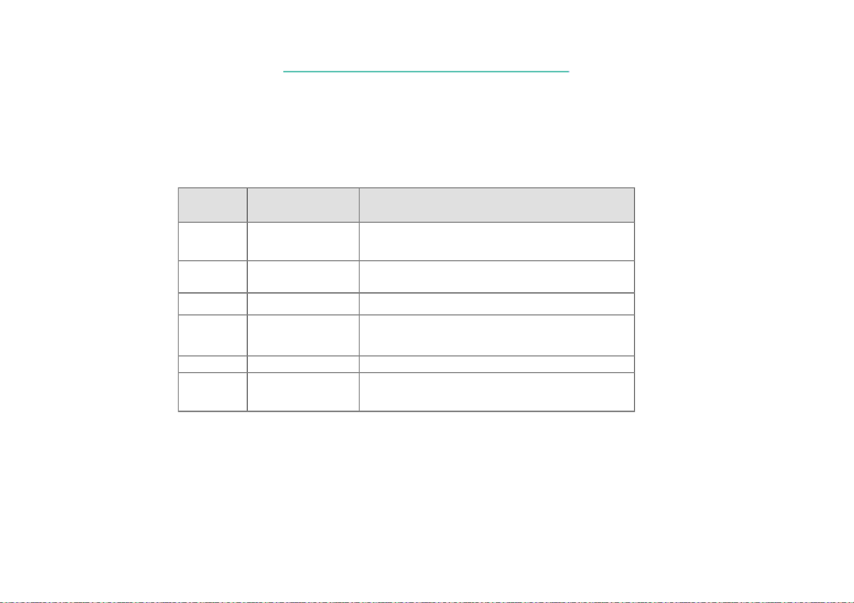
1.3 Other Functions
1.3.1 Hot Key Function
7321 N/B Maintenance7321 N/B Maintenance
Keys
Comb in ation
Fn + F5
Fn + F6 Brightness down
Fn + F7 Brightness up Increases the LCD brightness/No function in DSTN model
Fn + F10 Toggle Battery Warning on/off
Fn + F11 Panel Off/On Toggle Panel Off/On
Fn + F12
LCD/external CRT
switching
Enable/Disable
BatteryWarning Beep
Suspend to
DRAM/HDD
Feature Meaning
Rotate display mode in LCD only, CRT only and
si mult an eou sly
Decreases the LCD brightness/No function in DSTN
model
Force the computer into either Suspend to HDD or
Suspend to DRAM mode depending on BIOS Setup
32
Page 34

7321 N/B Maintenance7321 N/B Maintenance
1.3.2 Quick Key Function
Keys Feature Meaning
QSB1 Entertainment Quick
Key
QSB2 Instant Internet Determined by SW component
QSB3 My Presario Determined by SW component
QSB4 Search Determined by SW component
QSB5 Email Determined by SW component
1.3.3 Flash ROM (BIOS)
7321system utilizes the state-of-the-art Flash EEPROM technology.User can upgrade the system BIOS
in the future just running the program from MiTAC.
Determined by SW component
1.3.4 LED Indicators
System has nine status LED indicators to display system activity which include above keyboard and
below touch pad:
Three LED indicators below touch pad:
--AC POWER:
This LED lights green when the notebook is being powered by AC, and flash (on 1 second, off one
33
Page 35

7321 N/B Maintenance7321 N/B Maintenance
second) when Suspend to DRAM is active using AC power. The LED is off when the notebook is
off or powered by batteries, or when Suspend to Disk.
BATTERY POWER:
--
This LED lights green when the notebook is being powered by batteries, and flashes (on one second,
off one second) when suspend to DRAM is active using battery power. The LED is off when the
notebook is off or powered by AC, or when Suspend to Disk.
--BATTERY STATUS:
During normal operation, this LED stays off as long as the battery is charged. When the battery
charge drops to 10 % of capacity, the LED lights red, flashes per 1 second and beeps per 2 seconds.
When AC is connected, this indicator glows green if the battery pack is fully charged, or orange
(amber) if the battery is being charged
Six LED indicators above keyboard:
From left to right that indicates CD-ROM/MO, HARD DISK DRIVE, FLOPPY DISK DRIVE,
NUM LOCK, CAPS LOCK and SCROLL LOCK.
1.3.5 COM port assignment
COM1: MODEM/RS-232/Disable
.
34
Page 36

7321 N/B Maintenance7321 N/B Maintenance
COM2: IR/RS-232/Disable
1.3.6 Reset switch
There is a reset switch at bottom side of notebook. It will reset embedded controller H8 and turn off
system totally. This switch was used when H8 hangs up at that time you cannot turn system off.
1.3.7 CMOS Battery
CR2032 3V 220mAh lithium battery
When AC in or system main battery inside, CMOS battery will consume no power.
AC or main battery not exist, CMOS battery life depends on VT8231 RTC power consumption.
Battery was put in battery holder, can be replaced.
1.3.8 I/O Port
Bidirectional Parallel port (EPP/ECP)
VGA monitor port
PS/2 port (active at the same time)
FIR port
2 USB ports
35
Page 37

7321 N/B Maintenance7321 N/B Maintenance
Serial port
DC input
Microphone port
S-Video Out Port (NTSC/PAL) (Optional)
Line-in port
Line-out port (metal I/F; w/o S/PDIF)
RJ-45 port (Optional)
RJ-11 port (Optional)
36
Page 38

7321 N/B Maintenance7321 N/B Maintenance
1.4 Peripheral Components
7321 Peripheral Components
BRAND MODEL NAME
LCD PANEL Hyundai
Floppy Disk Drive Mitsumi D353G
HDD
CD-ROM Drive TEAC CD-224E-A92/B92
CDR-RW KME UJDA320/330
DVD-ROM drive Pioneer
Pointing Device Synaptics TM41PUM220
PCMCIA TI PCI1225PDV
Fax Modem Askey V1456VQL-P1
Hiyachi(2.5” 9.5mmH) 20GB— DK23BA-20
14.1”TFT XGA, HT14
8
ⅩDVD-ROM-DVD-K11TA
Ⅹ13-101
37
Page 39

7321 N/B Maintenance7321 N/B Maintenance
Appendix 1: VT8231 GPIO definiti ons
Group
Stra pping
GPI
Pin # Pin Name Multi Func. GPIO Group Pin Define i n 7321
F4
V3
W1
U3
V2
T3
U1
T2
F3
SA16
SUSA#
MCCS#
SA17
GPI0
GPI1
GPI2
GPI3
GPI4
GPI5
GPI6
GPI7
GPI8
0/1 - Dis abl e/ enable LPC ROM
0/1 - CPURST/INIT polarity 1 - Soc ket 462
0/1 - Enabl e/ di sable CPU FREQ strapping 1 - Disable F RE Q strap
0/1 - Enabl e/ di sable auto reboot
mux with Register setting
GPI0 N/A
GPI1 N/A
EXTSMI# N/A
RING# N/A
LID N/A
BATLOW# N/A
PME# N/A
SMBALT#
INT RUDER# N/A GPI8
N/A GPI7
default
0 - Disable L PC ROM
1 - Disabe auto reboot
GPI0
GPI1
EXTSMI#
WAKEUP#
GPI4
GPI5
PME# & SCI# (from H8)
38
Page 40

7321 N/B Maintenance7321 N/B Maintenance
Y3
Y11
V11
U10
W10
V4
Y8
V1
P3
K3
G5
GPI9
GPI10
GPI11
GPI12
GPI13
GPI14
GPI15
GPI16
GPI17
GPI18
GPI19
~f0_rx58<6>
APICCLK f0_rx58<6>
f4_rxe5<3>
HREQ1# ~f4_rxe5<3>
f4_rxe5<3>
HREQ2# ~f4_rxe5<3>
f4_rxe5<2>
LREQ1# ~f4_rxe5<2>
f4_rxe5<2>
LREQ2# ~f4_rxe5<2>
~f0_rx58< 7> & ~ f0_rx58< 6> MB_ID0
WSC# f0_rx58<7>
APIC R EQ# f0_rx58<6>
~f0_rx58< 5> & ~ f4_rxe5< 7> MB_ID1
LDRQ# f0_rx58<5>
ACSIN3 ~ f0_rx58< 5> & f4_rxe5<7>
CPUMISS N/A
f4_rx40<7> TH RM#
AOLGPI
TH R M ~f4_rx40<7>
GPO18 f4_rxe5<0>
FAN2 f4_rxe5<0>
SLPBTN# f4_rx40<6>
f4_rx40<7>
~f4_rxe5<0>
~f4_rxe4< 5> & ~ f4_rxe5< 1> GPI19
GPI9
PANEL_ID0
PANEL_ID1
PANEL_ID2
PANEL_ID3
CARD_IN#
GPI18
39
Page 41

W13
Y13
U7
T7
Y2
J5
R2
GPI20
GPI21
GPI22
GPI23
GPI24
GPI25
GPI26
7321 N/B Maintenance7321 N/B Maintenance
GPO 1 9 f4_rxe5<1> & f4_rxe4< 5>
ACSDIN2 ~f4_rxe4<5>
~f4_rxe4<6> &
pmio_rx4e<4>
GPO20 ~f4_rxe4<6>
LA20 f4_rxe4<6>
USBOC2# ~f4_rxe4<6> & pmi o_rx 4e<4>
~f4_rxe4<6> &
pmio_rx4e<5>
GPO21 ~f4_rxe4<6>
LA21 f4_rxe4<6>
USBOC3# ~f4_rxe4<6> & pmi o_rx 4e<5>
~f4_rxe4<7> &
pmio_rx4e<6>
GPO22 ~f4_rxe4<7>
IOR
GPO23 ~f4_rxe4<7>
IOW f4_rxe4<7>
GPO24 f4_rxe6<0>
GPIOA
GPO25 f4_rxe6<1>
GPIOC ~/f4_rxe6<1>
ATEST
GPO 2 6 f4_rx55<2> & f4_rx55< 3>
f4_rxe4<7>
~f4_rxe4<7> &
pmio_rx4e<7>
~f4_rxe6<0> GPI
~/f4_rxe6<0>
~f4_rxe6<1> GPI VGA_SUS ?
?
f4_rx55<2> &
~f4_rx55<3>
OD GPI20
OD
OD
OD IOW#
GPI C ARD_ACT#
SPK_OFF
IOR#
AGP_BUSY#
40
Page 42

7321 N/B Maintenance7321 N/B Maintenance
GPO
R1
G3
F1
Y1
W3
R4
P1
P2
GPI27
GPI28
GPI29
GPI30
GPI31
GPO0
GPO1
GPO2
SMBDT2
GPO27 f4_rx55< 2> & f4_rx55<3>
SMBCK2 ~f4_rx55<2>
JAB1 audi o ena & game ena
JBB1 audi o ena & game ena
GPO30 f4_rxe6<6>
GPIOD ~/f4_r xe6<6>
DTEST
GPO31 f4_rxe6<7>
GPIOE ~/f4_rxe6<7>
mux with Register setting
SLOWCLK f4_rx54[1-0]=01,10,11
SUSA# ~f4_rx54<2>
SUSB#
~f4_rx55<2>
f4_rx55<2> &
~f4_rx55<3>
audio ena & game di sa KB_US / JP #
audio ena & game di sa GPI29
~f4_rxe6<6> GPI
?
~f4_rxe6<7> GPI GPO31
f4_rx54[1-0] = 00 &
PMIO_rx4c[0]
f4_rx54<2> SUSA# SUSA#
f4_rx54<3> SUSB# SUSB#
~f4_rx54<3>
GPI
default
GPO0
GPO27
GPO30
SLOW CLK
41
Page 43
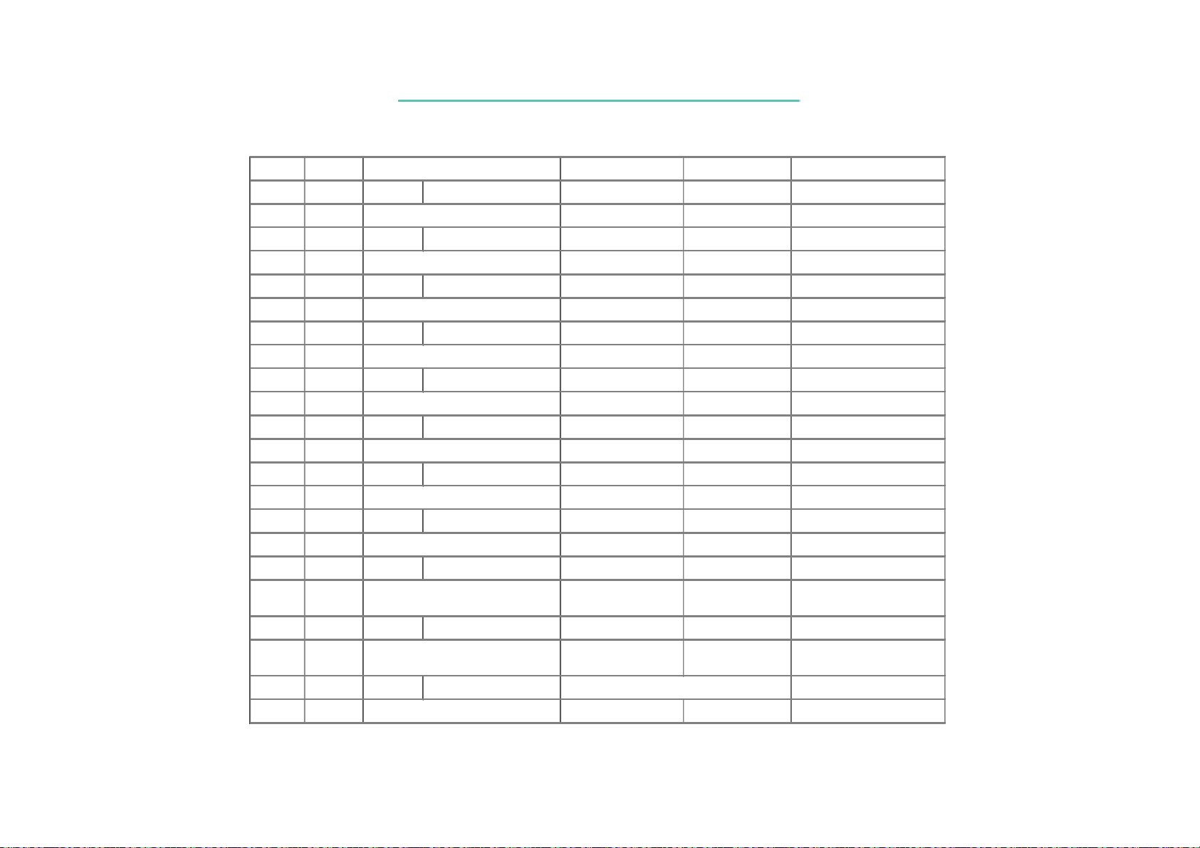
7321 N/B Maintenance7321 N/B Maintenance
N5
P4
T4
W11
T10
V10
H5
R8
GPO3
GPO4
GPO5
GPO6
GPO7
GPO8
GPO9
GPO10
GPO11
GPO12
GPO13
GPO14
f4_rx54<4> SUSSTAT# SUSSTAT#
SUSSTAT# ~f4_rx54<4>
f4_rx55<1> SUSCLK
SUSCLK ~f4_rx55<1>
f4_rxe4<0> CPUSTP# CPUST P#
CPUSTP# ~f4_rxe4<0>
f4_rxe4<1> PCISTP# PCISTP#
PCISTP# ~f4_rxe4<1>
f4_rxe4<4> SLP#
SLP# ~f4_rxe4<4>
f4_rxe5<3> HGNT1# RSTDRV# (reserved)
HGNT 1# ~f4_rxe5<3>
f4_rxe5<3> HGNT2# RS232_OFF#
HGNT 2# ~f4_rxe5<3>
f4_rxe5<2> LGNT1#
LGNT 1# ~f4_rxe5<2>
f4_rxe5<2> LGNT2# IR_MD0 (for distance)
LGNT 2# ~f4_rxe5<2>
f4_rxe5<4> &
~f0_rx53<7>
JAB2 f4_rxe5<4>
f4_rxe5<4> &
~f0_rx53<7>
JBB2 audio ena & game ena
f4_rxe5<5> IRTX IRTX
SUSCLKW2
SLP#U6
CARD_SUS#Y10
JAB2 GP012
JBB2
GPO13H4
42
Page 44
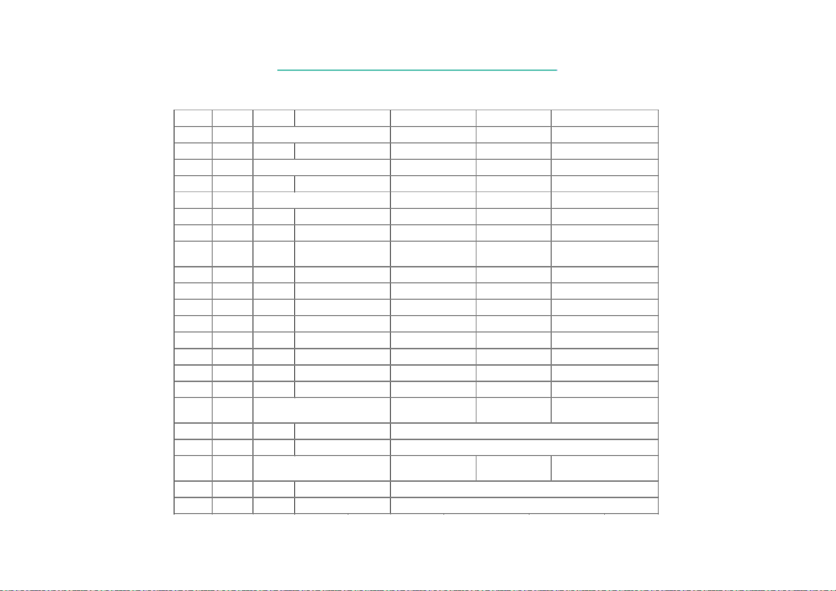
U8
Y6
W6
G5
W13
Y13
U7
T7
Y2
J5
R2
R1
W4
Y4
7321 N/B Maintenance7321 N/B Maintenance
IRTX ~f4_rxe5<5>
GPO15
GPO16
GPO17
GPO18
GPO19
GPO20
GPO21
GPO22
GPO23
GPO24
GPO25
GPO26
GPO27
GPO28
GPO29
IRRX
PCS0# ~f4_rxe4<2>
MCCS# ~f4_rxe4<3>
GPI18/FAN2/SLPBT
GPI19/ACSDIN2/PC
S1#
GPI20/LA20/USBOC
GPI21/LA21/USBOC
GPI22/IOR# see above
GPI23/IOW#
GPI24/GPIOA see above GPI AGP_B US Y #
GPI25/GPIOC/ATES
GPI26/S M B DT2 see above SM B DT2 CARD_ACT#
GPI27/SMBCK2
AP ICD0 ~f0_rx58< 7> & f0_rx58<6>
AP ICCS# f0_rx58<7> & ~f0_rx58< 6>
AP ICD1 ~f0_rx58< 7> & f0_rx58<6>
AP ICACK# f0_rx58<7> & ~ f0_rx 58< 6>
f4_rxe5<5> IRRX IRRX
~f4_rxe5<5>
f4_rxe4<2> PCS0# PCS0#
f4_rxe4<3> MCCS# MCCS#
see above
see above
see above
see above
see above
see above
~f0_rx58< 7> &
~f0_rx58<6>
~f0_rx58< 7> &
~f0_rx58<6>
FAN2 GP018K3
SDIN2 GPI19
SMBCK2 GPO27
PICD0 GPO28
PICD1
GPI GPI20
GPI SPK_OFF
GPI IOR#
GPIsee above
GPI RSET_TV
IOW#
GPO29
43
Page 45
7321 N/B Maintenance7321 N/B Maintenance
GPIO
Y1
Y2
T8
J5
Y1
W3
GPO30
GPO31
GPIOA
GPIOB
GPIOC
GPIOD
GPIOE
GPI30/GPIOD/DTEST
GPI31/GPIOE
IRRX2 FIR I/O Rx33 & 3 4
see above GPI
see above GPIW3
see above
see above
see above
see above
GPO30
GPO31
IRMODE
(for IR type)
44
Page 46
7321 N/B Maintenance7321 N/B Maintenance
1.5 Software Overview
1.5.1 BIOS features
Including System BIOS , VGA BIOS , POST , PM , PnP , ACPI
Support Shadow RAM BIOS feature
Support Boot Block feature
Support ACPI 1.0b
Support DMI 2.3
Support Quite Boot
Support AMD PowerNow! Technology
Support ACPI Power Management S0, S1, S3, S4 , S5
Operating Systems Support
OS
Microsoft Windows98 SE
Microsoft Windows ME
Microsoft Windows 2000
ACPI
YES YES YES
YES YES YES
YES YES YES
Support
WHQL
45
Page 47

7321 N/B Maintenance7321 N/B Maintenance
USB Fl
1.5.2 USB Legacy Support
USB Legacy Suppor t
Device DOS Mode Resume from S1 Resume from S3 Resume from S4
NO NO NO NO
1.6 BIOS Function Description
1.6.1 CMOS Setup
1.6.1.1 Main Menu
The Main pull-down menu contains the basic configuration setting of the system like “ Date and
Time “ ,“Boot Sequence”,”Internal Numlock” refer to the BIOS SCU for the detail setting
1.6.1.2 Advance Menu
The Advance pull-down menu contains the I/O configuration setting of the system like “COM
Ports“, ”LPT Port “, “Shared Video Memory “ . Please refer to the BIOS SCU for the detail setting
1.6.1.3 Security Menu
The Security pull-down menu contains the security setting which safeguard your system against
unauthorized use like “ Set Password “ , “Hard Disk Boot Sector“ . Please refer to the BIOS SCU
for the detail setting .
46
Page 48

7321 N/B Maintenance7321 N/B Maintenance
1.6.1.4 Exit Menu
The Exit pull-down menu displays ways of exiting SCU , after finished with your settings , you
must save and exit SCU so that the settings can take effect . Please refer to the BIOS SCU for the
detail Setting .
1.6.2 Power Management
1.6.2.1 Component Level Power Management Status :
Global power state G0 Working G1 Sleep G2 Soft off
Sleep state S0 S3 S4 S5
CPU
VIA TwisterK VGA
VIA VT8231 Audio
VIA VT8231 Modem
VIA VT8231 LAN
VIA VT8231 USB
Hard Drive
CD-ROM
TI1420 Card Bus
Audio AMP
ICS9248-189 Clock Gen
H8 KBC
C0 POWER OFF POW ER OFF POWER OFF
D0 D3 POW ER OFF POWER OFF
D0 D3 POW ER OFF POWER OFF
D0 D3 POW ER OFF POWER OFF
D0 D3 POW ER OFF POWER OFF
D0 D3 POW ER OFF POWER OFF
D0 D3 POW ER OFF POWER OFF
D0 D3 POW ER OFF POWER OFF
D0 D3 POW ER OFF POWER OFF
POW ER ON POWER DOWN POWER OFF POWER OFF
POW ER ON POWER ON POWER OFF POWER OFF
POW ER ON POWER DOWN POWER OFF POWER OFF
47
Page 49
7321 N/B Maintenance7321 N/B Maintenance
Flop
1.6.2.2 The Behavior about Component Level Power Management
Component activity is
Component Activity
VIA TwisterK VGA Can not wake system Monitored by driver
VIA VT8231 Audio Can not wake system Monitored by driver
Modem Device
LAN Device Can not wake system Monitored by driver
Hard
Drive Can not wake system Monitored by OS
CD/DVD playback Can not wake system Monitored by driver
USB Device Can not wake system Monitored by driver
Touch Pad Can not wake system Monitored by OS
H8 KBC Can wake system Monitored by KBC/EC
The capability of Wake
upsystem from S3 state
Wakeup by incoming call
ifapplication is enabled
Can not wake system Monitored by OS
monitored,preventing
timeout to enter sleep
state
Monitored by driver
1.6.3 OEM special functions
1.6.3.1 Cover Switch
At ACPI mode there are there functions to be chosen at windows power management of control
panel.
48
Page 50

7321 N/B Maintenance7321 N/B Maintenance
1. None
2. Standby
3. Hibernation
4. Power Off
1.6.3.2 Power Button
At ACPI mode. Power button behavior was set by windows power management of control panel.
1. Standby
2. Hibernation
3. Power Off
Continue pushing power button over 4 seconds will force system off at ACPI mode.
1.6.4 Security functions
1.6.4.1 Power-On Password
The Power-On password item allows you to set the password for your system . The password is
required for starting up the system
1.6.4.2 BootSctor Protect
The Bootsector protect prevent computer viruses by protecting the hard disk boot sector from any
change .
49
Page 51

7321 N/B Maintenance7321 N/B Maintenance
1.6.5 Identification
1.6.5.1 SSID / SSVID
SSID : 7321 h
SSVID : 1071h
1.6.5.2 System LOGO Master ID
Master
ID :XXXXXX
1.7 Driver / Utility Description
1.7.1 Device Driver Suppor t
Win98SE Win2000 WinMe Certification
VGA YES YES YES YES
Audi o Y ES YES YES YES
PCMCIA YES YES YES YES
Modem YES YES YES YES
LAN YES YES YES YES
Touchpad YES YES YES YES
50
Page 52
7321 N/B Maintenance7321 N/B Maintenance
2 System View and Disassembly
2.1 System View
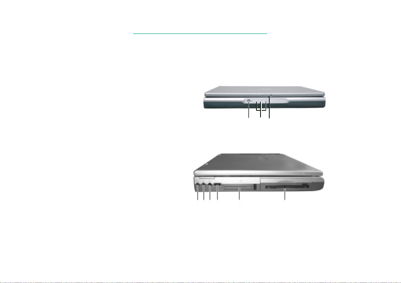
2.1.1 Front View
Mail-Received Button/Indicator
Power Indicators
Top Cover Latch
2.1.2 Left-Side View
Audio Input Connector
Microphone Connector
Audio Output Connector
Volume Control
PC Card Slots
Floppy Disk Drive
11112
11112222333344445
56
55
23333
22
6
66
51
Page 53
7321 N/B Maintenance7321 N/B Maintenance
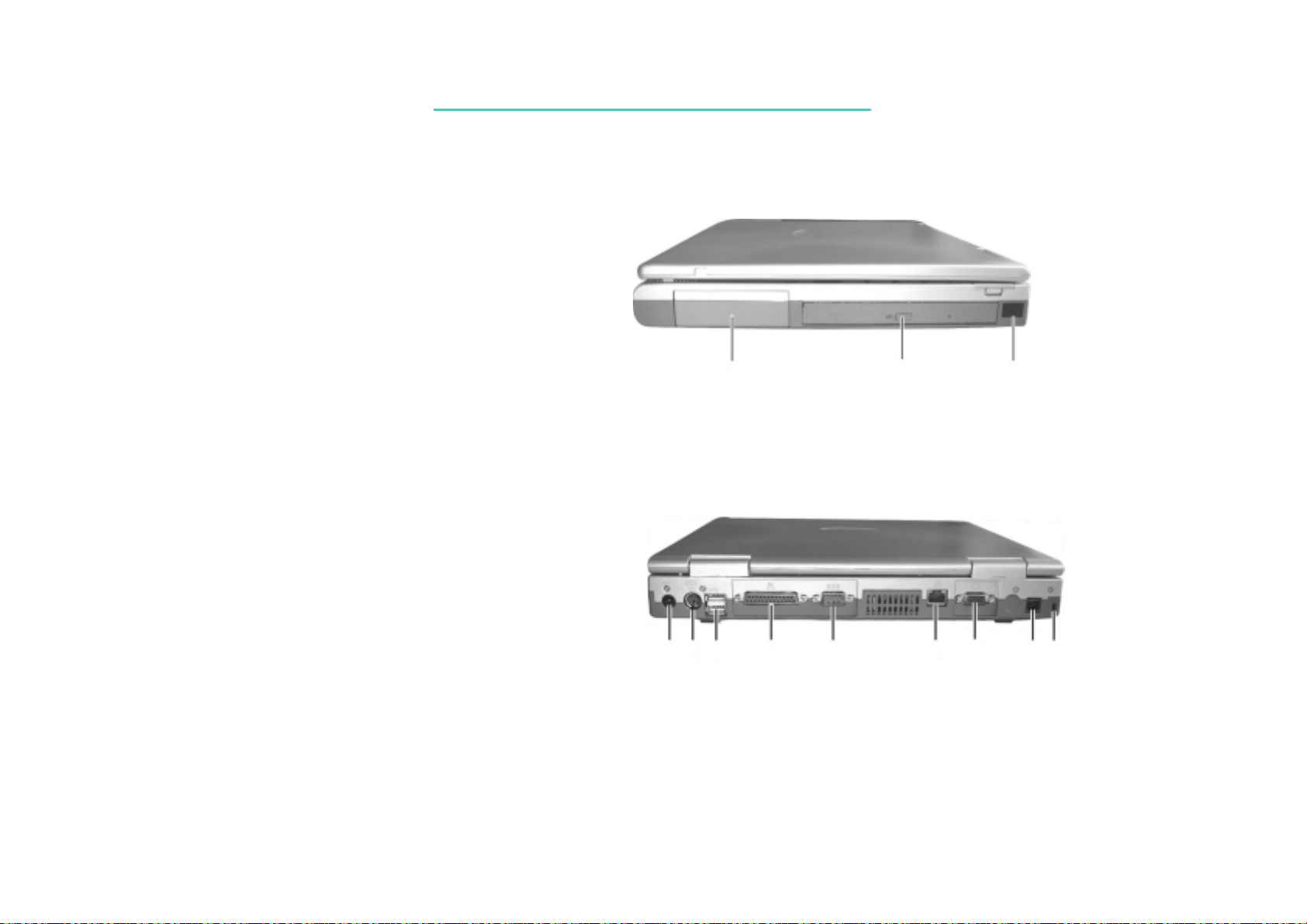
2.1.3 Right-Side View
Battery Pack
CD-ROM/DVD-ROM Drive
IR Port
2.1.4 Rear View
Power Connector
PS/2 Port
USB Ports
Parallel Port
Serial Port
RJ-45 Connector
VGA Port
333322221111
RJ-11 Connector
Kensington Lock
1111222233334
45
44
56
55
67
78
66
77
89999
88
52
Page 54

7321 N/B Maintenance7321 N/B Maintenance
2.1.5 Bottom View
CPU Cover
Modem Card Cover
FDD/HDD Module
Battery Pack
2.1.6 Top-O pen View
LCD Screen
Power Button
Keyboard
Easy Start Buttons
Touchpad
11112
4444
2
22
3333
Stereo Speaker Set
1
2
3
6
4
5
53
Page 55
7321 N/B Maintenance7321 N/B Maintenance
2.2 System Disassembly
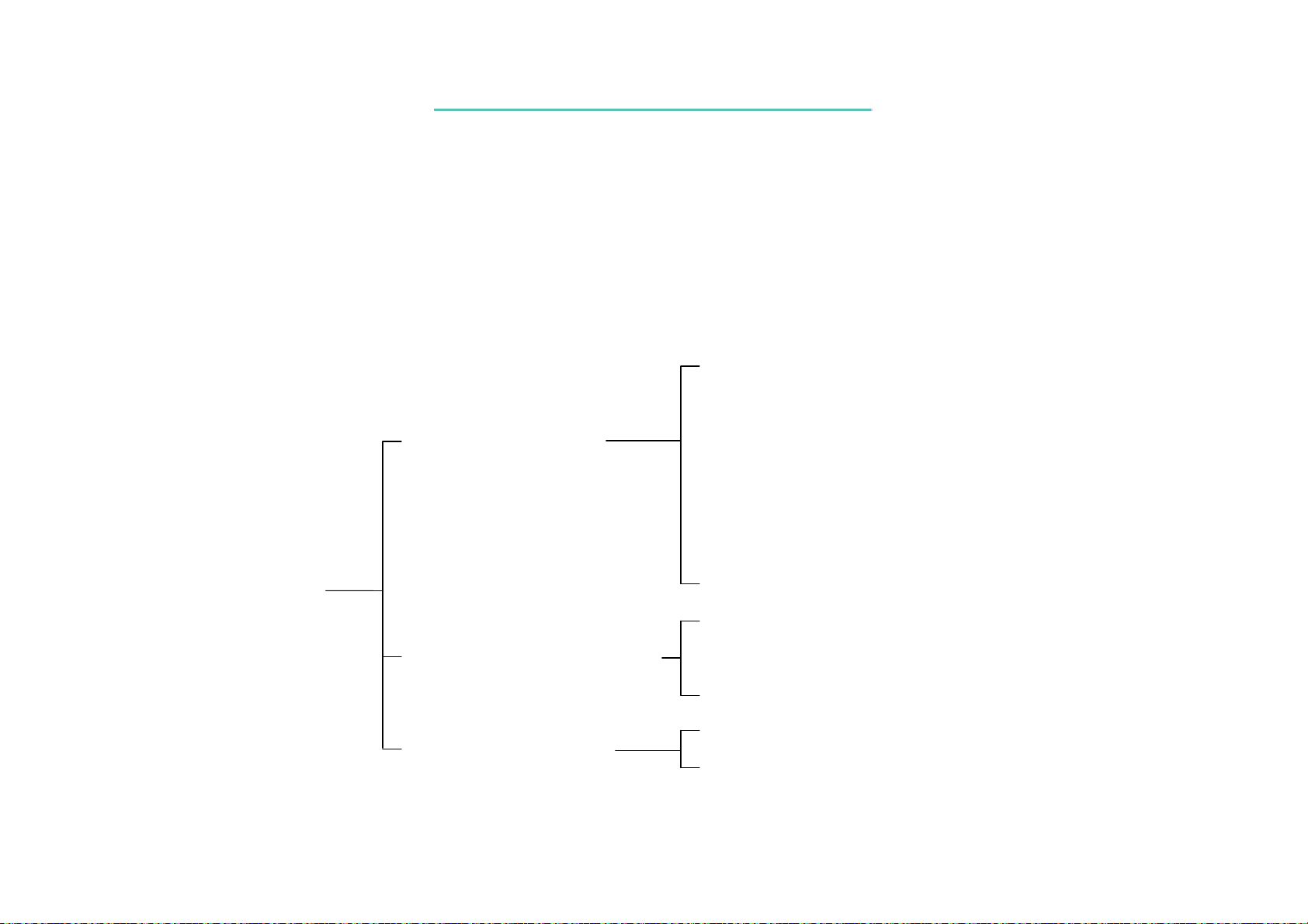
The section discusses at length each major component for disassembly/reassembly and show corresponding
illustrations. Use the chart below to determine the disassembly sequence for removing components from the
notebook.
NOTE: Before you start to install/replace these modules, disconnect all peripheral devices and make sure the
notebook is not turned on or connected to AC power.
2.2.1 Battery Pack
2.2.2 CPU
NOTEBOOK
Modular Components
LCD Assembly Components
Base Unit Components
2.2.3 Modem Card
2.2.4 FDD/HDD Module
2.2.5 CD-ROM Drive
2.2.6 Keyboard
2.2.7 SO-DIMM
2.2.8 LCD Assembly
2.2.9 LCD Panel
2.2.10 Inverter Board
2.2.11 System Board
2.2.12 Touchpad
54
Page 56
7321 N/B Maintenance7321 N/B Maintenance
2.2.1 Battery Pack
Disassembly
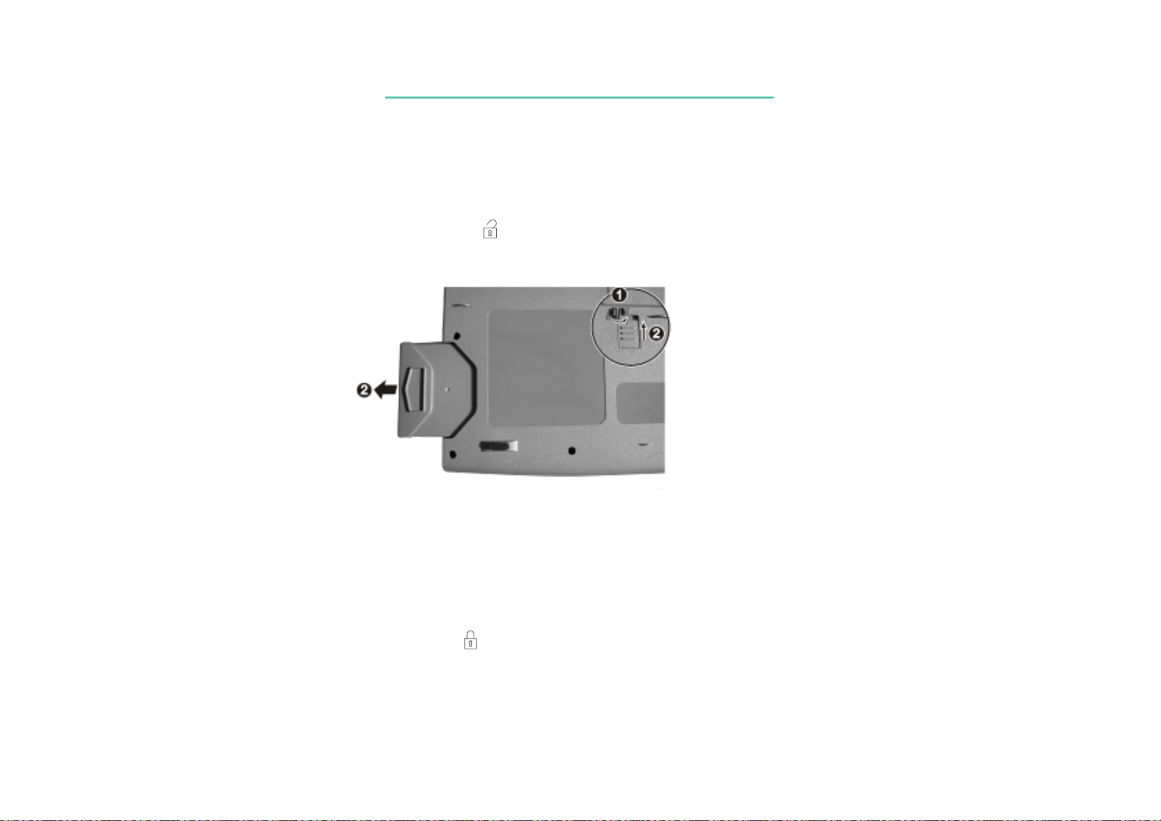
1. Carefully put the notebook upside down.
2. Turn the locking button to the "unlock” ( ) position (), then slide and hold the latch in the
unlock position and pull the battery pack out of the compartment ().(figure 2-3)
Figure 2-3
Reassembly
1. Push the battery pack into the compartment. The battery pack should be correctly connected
when you hear a clicking sound.
2. Turn the locking button to the "lock” ( ) position.
55
Page 57
7321 N/B Maintenance7321 N/B Maintenance
2.2.2 CPU
Disassembly
1. Carefully put the notebook upside down.
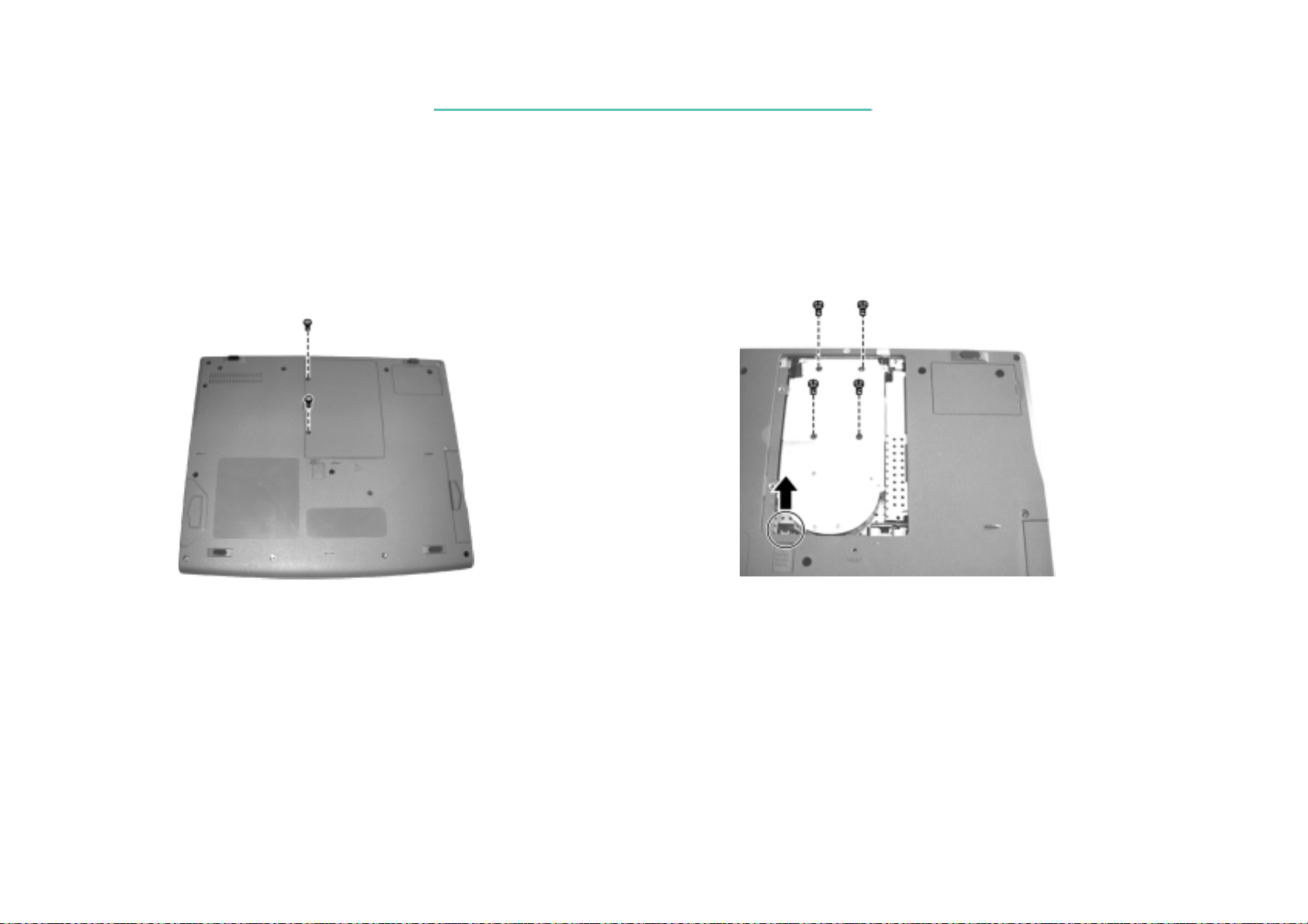
2. Remove two screws locking the CPU compartment cover, and then lift the cover up. (figure 2-4)
Figure 2-4 Figure 2-5
3. Remove four screws fastening the heatsink and disconnect the fan’s power cord to free the heatsink
from the CPU module. (figure 2-5)
56
Page 58
7321 N/B Maintenance7321 N/B Maintenance
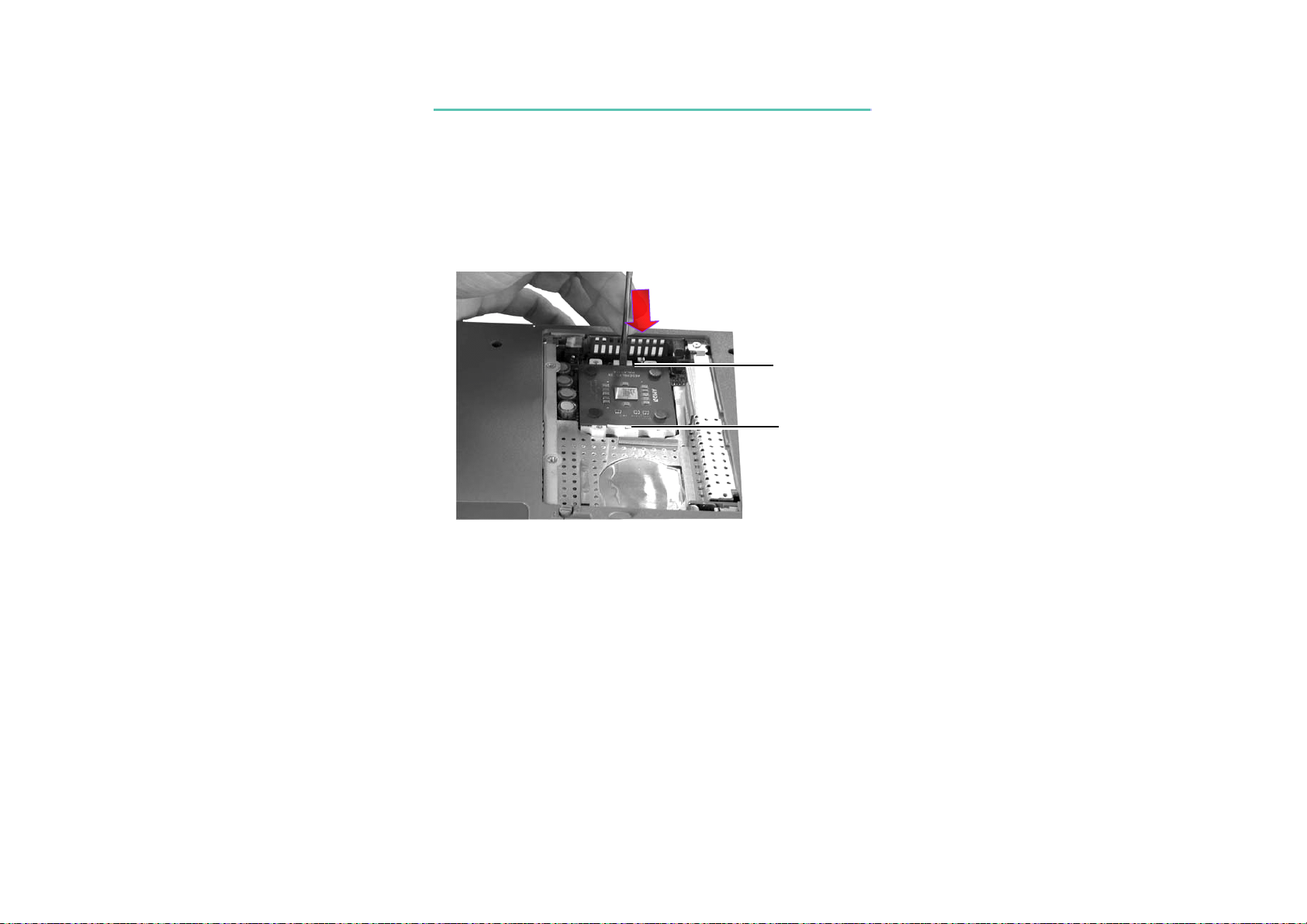
4. Insert a minus screwdriver 101 (JIS standard) into the “OPEN” hole of the socket, and push the screwdriver
toward the CPU to free the CPU. Now you can take out the CPU from the socket. (figure 2-6)
Open
Close
Figure 2-6
Reassembly
1. Align the arrowhead corner of the CPU with the beveled corner of the socket, and insert the CPU pins
into the holes. Insert the flat screwdriver into the “CLOSE” hole of the socket, and push the screwdriver
toward the CPU to secure the CPU in place.
2. Connect the fan’s power cord to the system board, fit the heatsink onto the top of the CPU and secure with
four screws.
3. Replace the CPU compartment cover and secure with two screws.
57
Page 59
7321 N/B Maintenance7321 N/B Maintenance
2.2.3 Modem Card
Disassembly
1. Carefully put the notebook upside down.
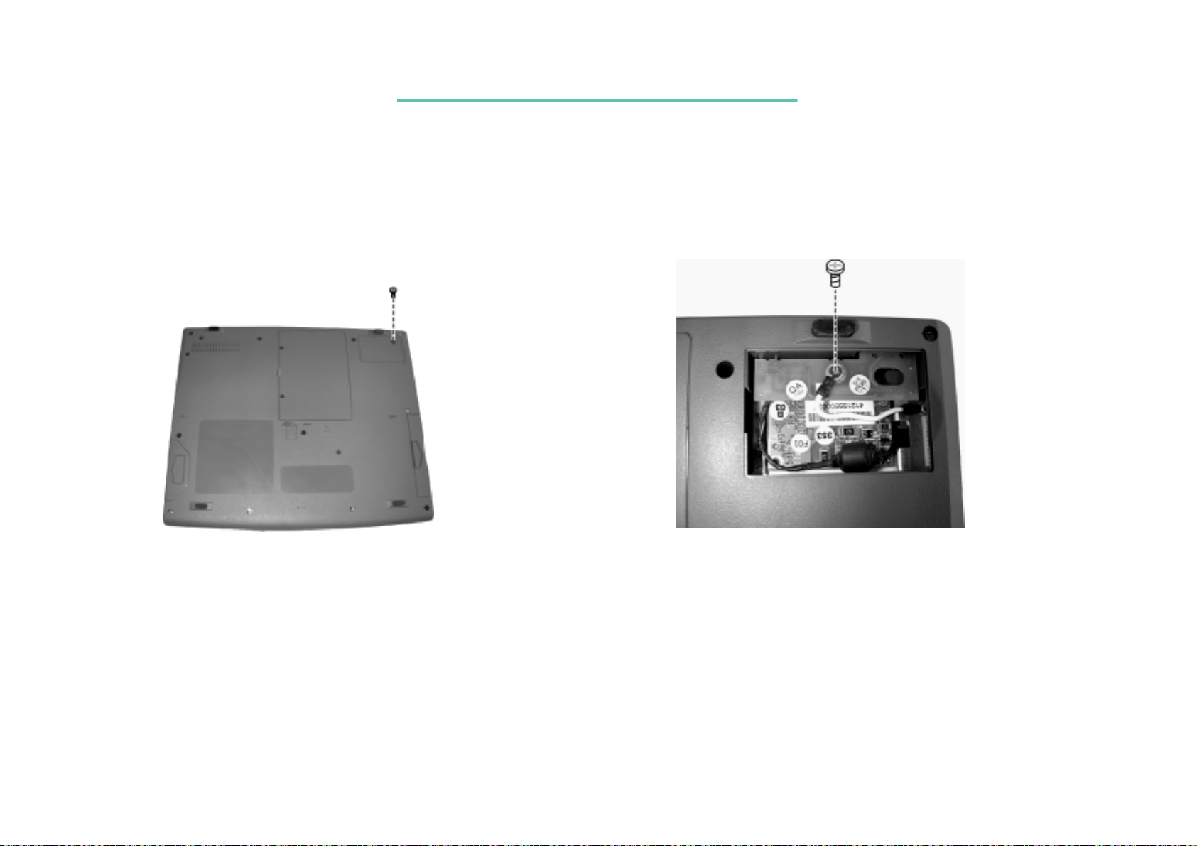
2. Remove one screw locking the modem card compartment cover, and then lift the cover up. (figure 2-7)
Figure 2-7 Figure 2-8
3. Remove one screw fastening the connector board and the grounding cable. (figure 2-8)
58
Page 60
7321 N/B Maintenance7321 N/B Maintenance
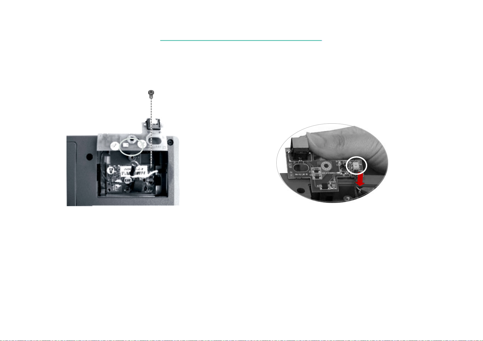
4. Slightly lift up the connector board, and then remove two screw fastening the modem card. Now you can take
out the modem card from the compartment. (figure 2-9)
5. And then disconnect the cable from connector board . (figure 2-10)
Figure 2-9 Figure 2-10
Reassembly
1. Reconnect the modem card into the system board and secure with two screws.
2. Hold the connector board an angle so that the phone line connector is pointed towards the opening on the
notebook. Insert the connector into the opening and secure with a screw which fastening both the connector
board and the grounding cable.
3. Replace the compartment cover and secure with one screw.
59
Page 61

7321 N/B Maintenance7321 N/B Maintenance
2.2.4 FDD/HDD Module
Disassembly
1. Carefully put the notebook upside down.
2. Remove one screw and slide the FDD/HDD module out of the compartment. (figure 2-11)
Figure 2-11
60
Page 62

7321 N/B Maintenance7321 N/B Maintenance
3. To take the hard disk drive apart, remove two screws of the hard disk. Then lift the hard disk up and unplug
the connector to remove it. (figure 2-12)
Figure 5-12 Figure 5-13
4. Remove four screws to separate the hard disk drive from the metal shield. (figure 2-13)
61
Page 63
7321 N/B Maintenance7321 N/B Maintenance
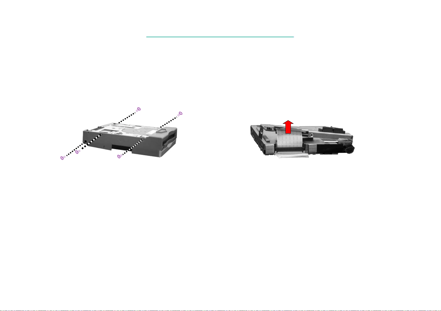
5. Remove five screws to separate the FDD module from plastic shield .(figure 2-14)
6. And then , disconnect the cable after peel off the adhesive tape.On this way,you can separate F DD module .
(Figure 2-15)
Figure 2-14
Figure 2-15
Reassembly
1. Reconnect the cable and conglutinate the adhesive tape.
2. Place FDD disk in the plastic shield and secure with two screws .
3. To install the hard disk drive, place it in the bracket and secure with four screws.
4. Connect the hard disk to the connector on the FDD/HDD module and secure with two screws.
5. Slide the FDD/HDD module into the compartment and secure with one screw.
62
Page 64
7321 N/B Maintenance7321 N/B Maintenance
2.2.5 CD-ROM Drive
Disassembly
1. Carefully put the notebook upside down.
2. Remove the battery pack. (See section 2.2.1 Disassembly.)
3. Remove the modem card. (See section 2.2.3 Disassembly.)
4. Remove the FDD/HDD module. (See step 2 in section 2.2.4 Disassembly.)
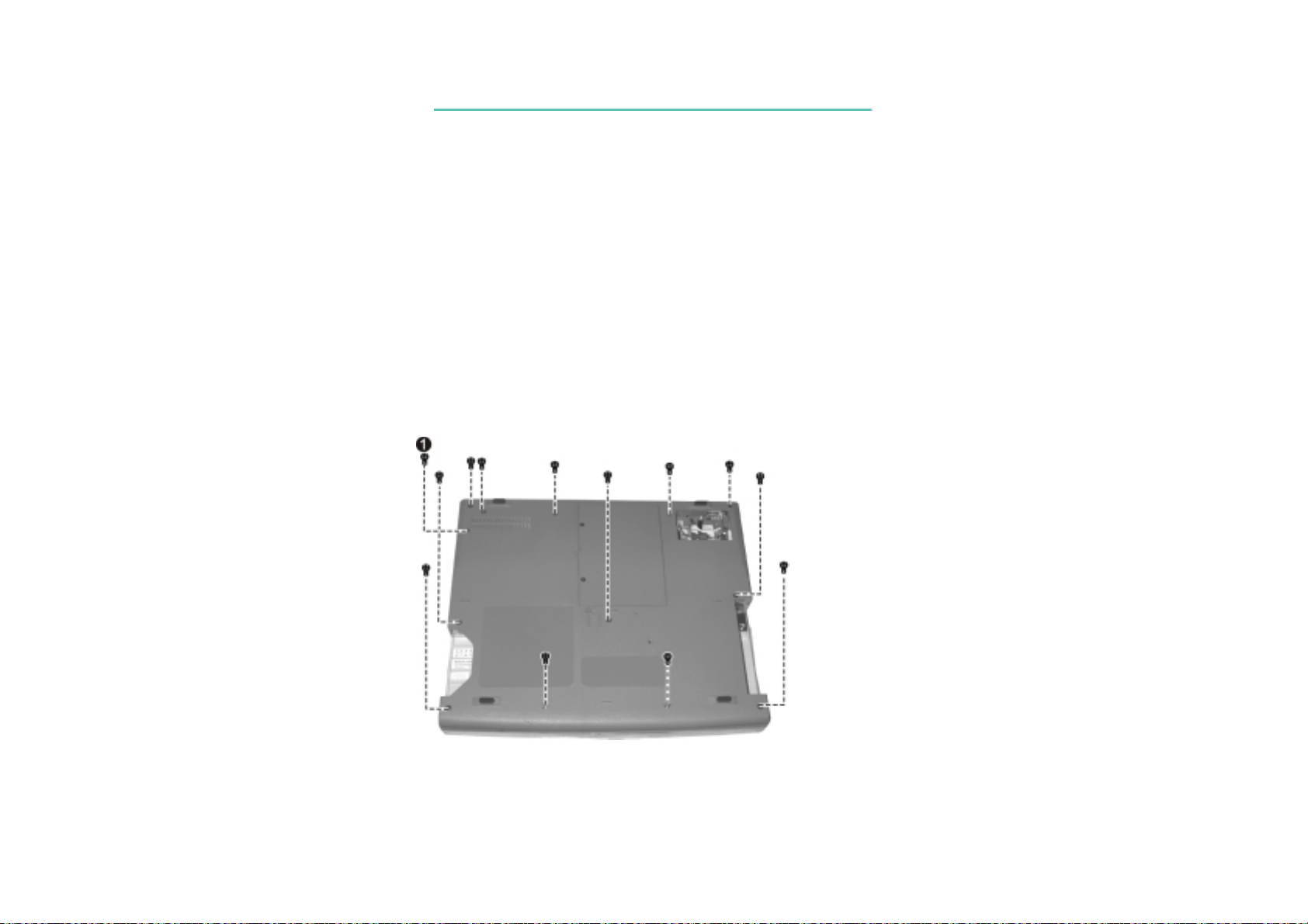
5. Remove one screw locking the CD-ROM (), and then the other twelve screws locking the base unit frame.
(figure 2-16) Now you can lift the base unit frame up.
Figure 2-16
63
Page 65
7321 N/B Maintenance7321 N/B Maintenance
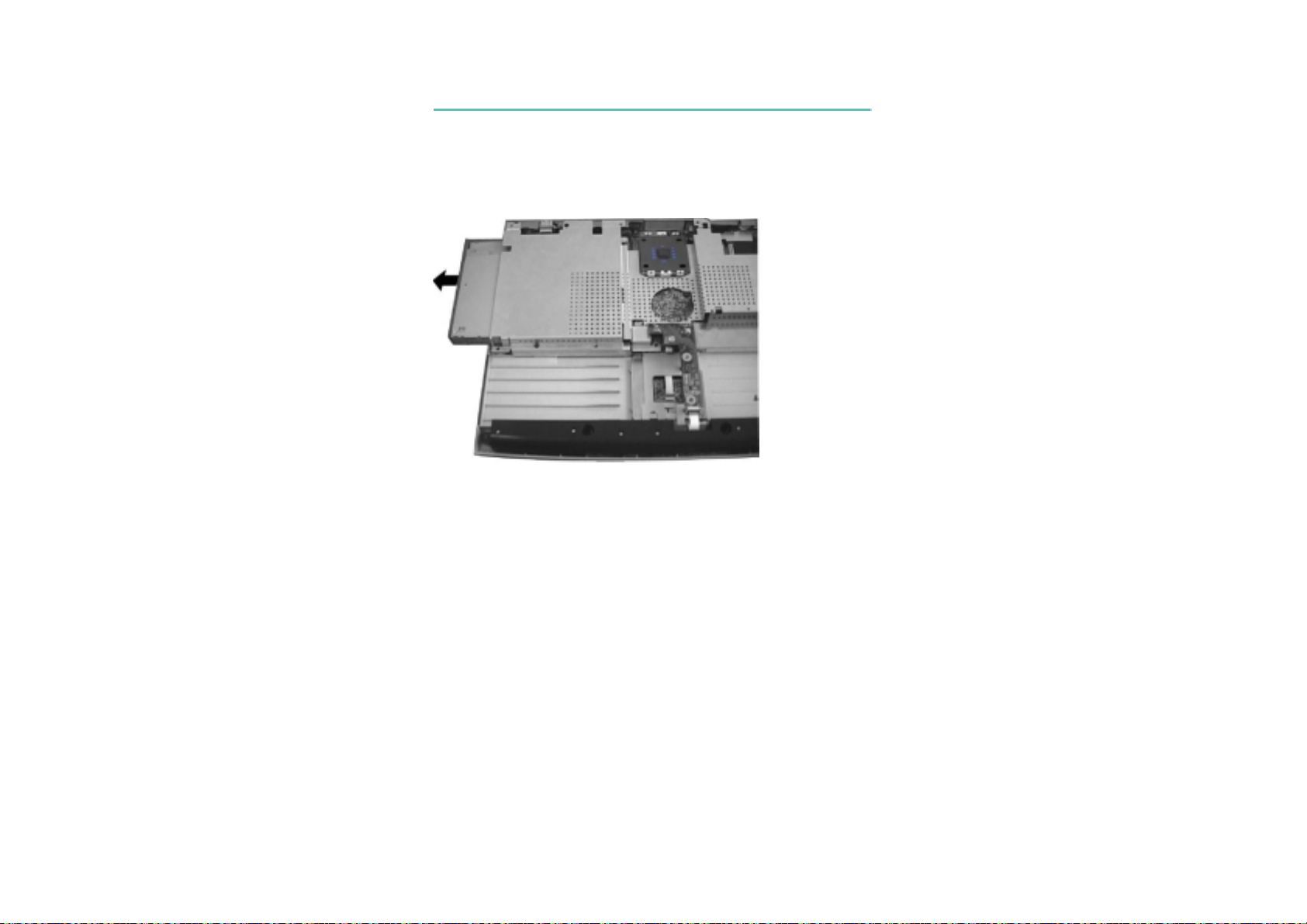
6. Hold the CD-ROM drive and slide it outward carefully. (figure 2-17).
Figure 2-17
Reassembly
1. Push the CD-ROM drive into the compartment.
2. Replace the base unit frame and secure with thirteen screws (includes one locking the CD-ROM drive).
3. Replace the FDD/HDD module. (See section 2.2.4 Reassembly.)
4. Replace the modem card. (See section 2.2.3 Reassembly.)
5. Replace the battery pack. (See section 2.2.1 Reassembly.)
64
Page 66

7321 N/B Maintenance7321 N/B Maintenance
2.2.6 Keyboard
Disassembly
1. Open the top cover.
2. Press the locking latch downward to unlatch the Easy Start panel () , push it leftward and lift it up from the
left side (). (figure 2-18)
Figure 2-18 Figure 2-19
3. Slightly lift up the keyboard and disconnect the cable from the system board to detach the keyboard.
(figure 2-19)
Reassembly
1. Reconnect the keyboard cable and fit the keyboard back into place.
2. Replace the Easy Start panel.
65
Page 67

7321 N/B Maintenance7321 N/B Maintenance
2.2.7 SO-DIMM
Disassembly
1. Remove the keyboard to access the SO-DIMM sockets. (See section 2.2.6 Disassembly.)
2. Pull the retaining clips outwards () and remove the SO-DIMM (). (figure 2-20)
Figure 2-20
Reassembly
1. To install the SO-DIMM, match the SO-DIMM's notched part with the socket's projected part and firmly
insert the SO-DIMM into the socket at 20-degree angle. Then push down until the retaining clips lock the SODIMM into position.
2. Replace the keyboard and the Easy Start panel. (See section 2.2.6 Reassembly.)
66
Page 68

7321 N/B Maintenance7321 N/B Maintenance
2.2.8 LCD Assembly
Disassembly
1. Open the top cover and remove the Easy Start panel. (See steps 1 to 2 in section 2.2.6 Disassembly.)
2. Remove the two hinge covers by inserting a flat screwdriver to the rear of the cover and pry the cover out.
(figure 2-21)
Figure 2-21 Figure 2-22
3. Open the top cover. Unplug the three cable connectors coming from the LCD assembly, and remove four
screws of the hinges. Now you can separate the LCD assembly from the base unit. (figure 2-22)
Reassembly
1. Attach the LCD assembly to the base unit and secure with four screws on the hinges.
2. Reconnect the LCD cable connectors to the system board.
3. Replace the two hinge covers.
4. Replace the Easy Start panel.
67
Page 69

7321 N/B Maintenance7321 N/B Maintenance
2.2.9 LCD Panel
Disassembly
1. Remove the LCD assembly. (See section 2.2.8 Disassembly.)
2. Remove the two rubber pads and two screws on the lower part of the panel. (figure 2-23)
Figure 2-23 Figure 2-24
3. Insert a flat screwdriver to the lower part of the frame and gently pry the frame out.Repeat the process until
the frame is completely separated from the housing.
4. Remove the four screws on the two sides of the LCD panel, and unplug the cable fro the inverter board.
(figure 2-24)
Reassembly
1. Fit the LCD panel back into place and secure with four screws, and reconnect the cable to the inverter board.
2. Fit the LCD frame back into the housing and replace the two screws and two rubber pads.
3. Replace the LCD assembly. (See section 2.2.8 Reassembly.)
68
Page 70
7321 N/B Maintenance7321 N/B Maintenance
2.2.10 Inverter Board
Disassembly
1. Remove the LCD assembly and detach the LCD frame (see instructions in previous two sections).
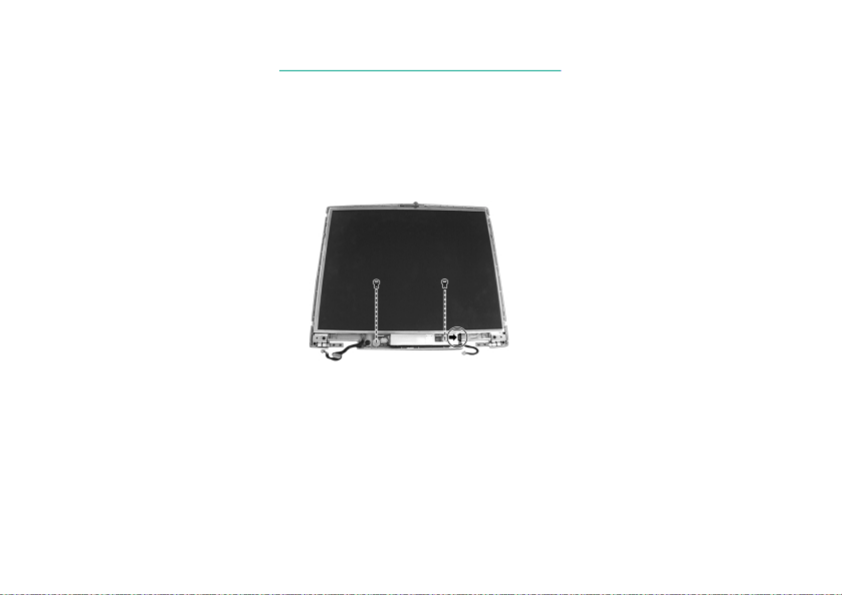
2. To remove the inverter board at the bottom side of the LCD assembly, unplug the cable and remove the two
screws. (figure 2-25)
Figure 2-25
Reassembly
1. Fit the inverter board back into place and secure with two screws.
2. Reconnect the cables.
3. Replace the LCD frame. (See section 2.2.9 Reassembly.)
4. Replace the LCD assembly. (See section 2.2.8 Reassembly.)
69
Page 71

7321 N/B Maintenance7321 N/B Maintenance
2.2.11 System Board
Disassembly
1. Remove the Keyboard. (See section 2.2.6 Disassembly.)
2. Remove the LCD assembly. (See section 2.2.8 Disassembly.)
3. Remove seven screws, and then take out the Easy Start board. (figure 2-26)
Figure 2-26 Figure 2-27
4. Remove four screws on the rear side of the notebook. (figure 2-27)
5. Remove the battery pack, heatsink, modem card, FDD/HDD module, and CD-ROM drive. (See section 2.2.1
to 2.2.5 Disassembly.)
70
Page 72
7321 N/B Maintenance7321 N/B Maintenance
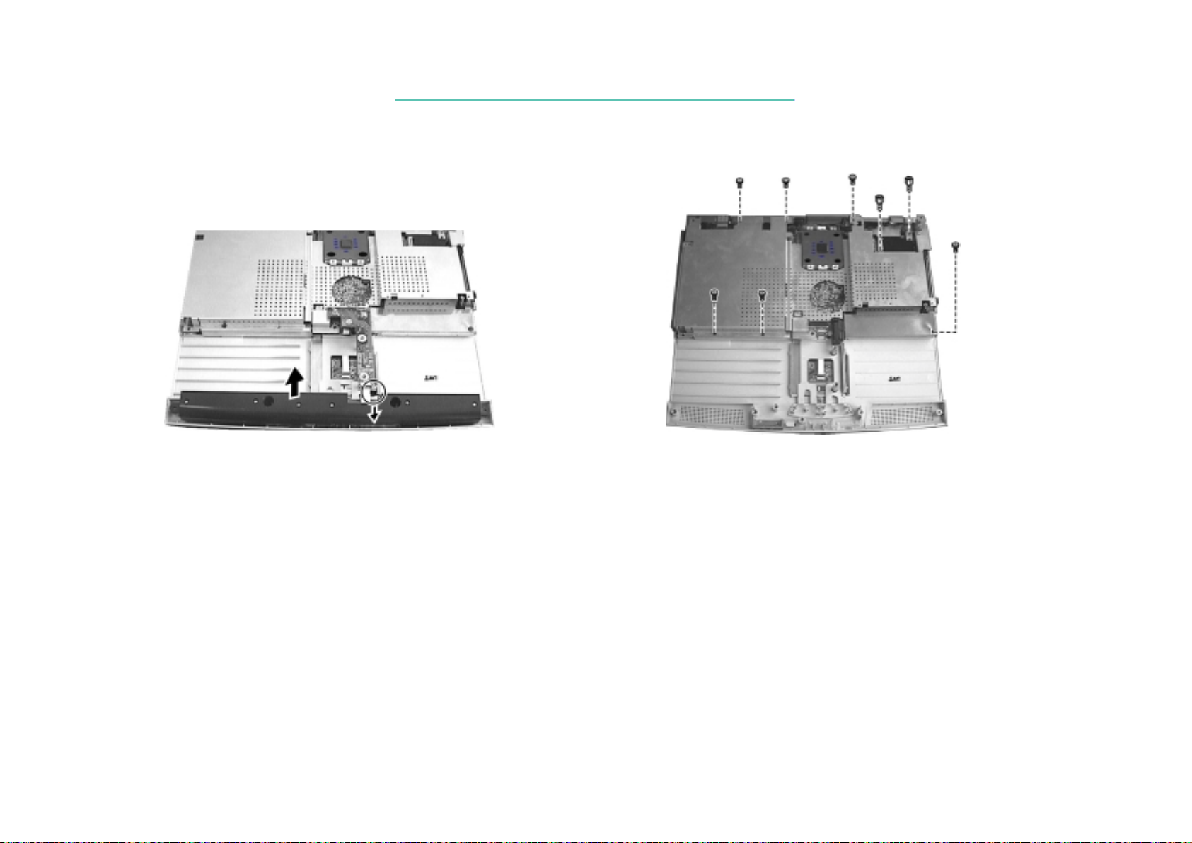
6. Lift up the speaker assembly and disconnect the cable. (figure 2-28)
Figure 2-28 Figure 2-29
7. Remove six screws and two hexnut screws fastening the metal shield, and then lift the shield up from the
system board carefully. (figure 2-29)
71
Page 73
7321 N/B Maintenance7321 N/B Maintenance
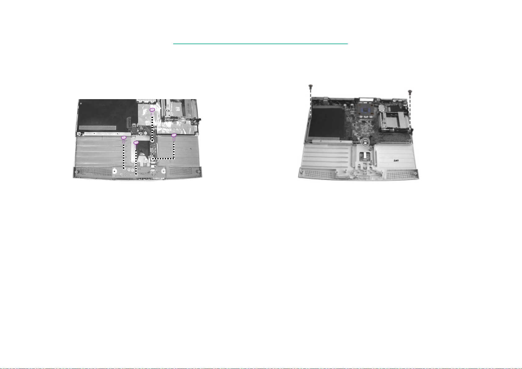
8. Remove four screws to take the recharge board apart. (figure 2-30)
Figure 2-30 Figure 2-31
9. Remove two screws fastening the system board and disconnect the cable of the touchpad. Now you can lift
the system board up from the base unit. (figure 2-31)
Reassembly
1. Fit the system board into place and secure with two screws.
2. Reconnect the touchpad’s cable.
3. Replace the metal shield and secure with six screws and two hexnut screws.
4. Replace the recharge board and secure with four screws.
5. Replace the speaker assembly and reconnect the cable.
72
Page 74

7321 N/B Maintenance7321 N/B Maintenance
6. Replace the base unit frame and secure with twelve screws.
7. Replace the battery pack, heatsink, modem card, FDD/HDD module, and CD-ROM drive.
8. Secure the four screws on the rear side of the notebook.
9. Put the notebook back to the upright position. Replace the Easy Start board into the housing, then secure with
seven screws.
10. Replace the LCD assembly.
11. Replace the keyboard and Easy Start panel.
73
Page 75
7321 N/B Maintenance7321 N/B Maintenance
2.2.12 Touchpad
Disassembly
1. Remove the system board. (See section 2.2.11 Disassembly.)
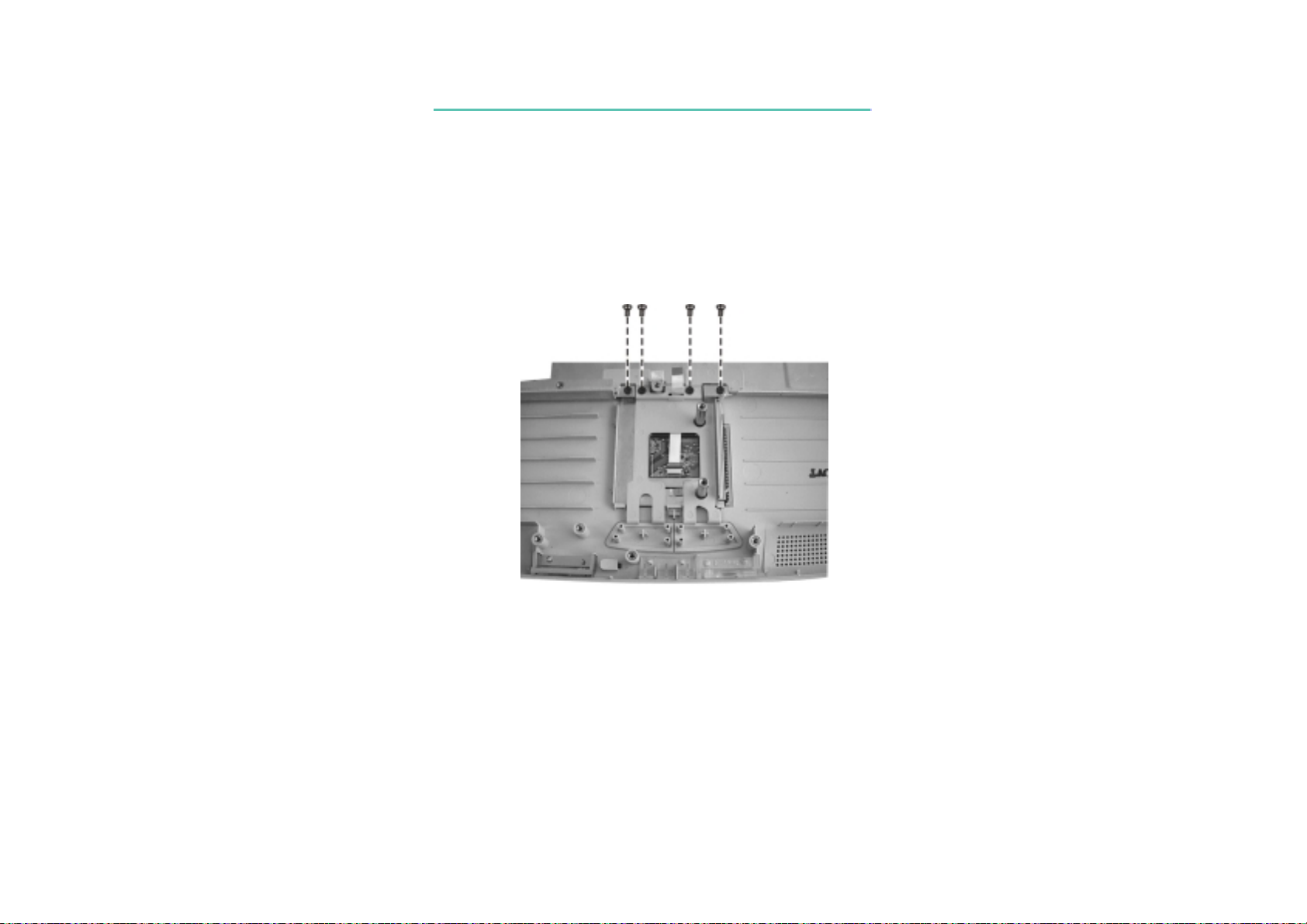
2. Remove the four screws to lift up the touchpad holder and touchpad panel. (figure 2-33)
Figure 2-32
Reassembly
1. Replace the touchpad holder and touchpad panel, and secure with four screws.
2. Replace the system board
and assemble the notebook. (See sectio n 2.2.11 Reassembly.)
74
Page 76
7321 N/B Maintenance7321 N/B Maintenance
3. Definition & Location Of Connectors/switches
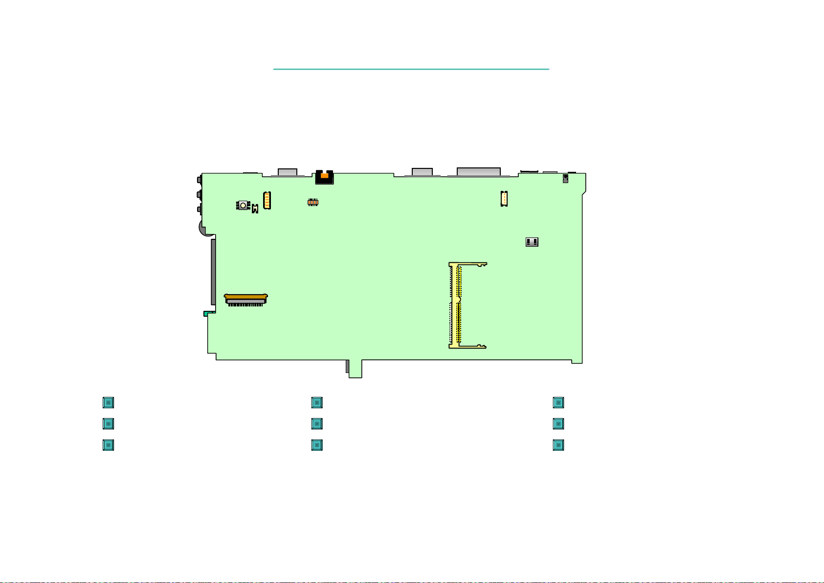
3.1 Mother Board-a
SW1
J2: External MIC-in connector
J3: LCD panel connector.
J4: Quick key transfer BD connector.
J3
J2
J8
J4
J5: Inverter BD connector
J7: 144 pins expansion SDRAM socket.
J8: Internal keyboard connector.
J5
SW3
J7
SW2
SW1: Power button.
SW2: Cover Suspend SW.
SW3: Frequency Jump setting
75
Page 77

7321 N/B Maintenance7321 N/B Maintenance
3. Definition & Location Of Connectors/switches
3.2 Mother Board-b
J509
J507
PJ501
U501
PJ501: Power jack ( AC adapter).
J501: Line In
J506 J505
J513
J507: PS/2 Mouse/keyboard
J508: MIC In
J512
J514
J516
U503
J515
J504
BT501
J503
J502
J501
J508
J510
J511
VR501
U509
J514: Charger & Touch-Pad connector
J515: HDD/FDD Connector.
J502: TV Out Port
J503: SIO Port.
J504: LAN connector
J505: VGA Connector.
J506: Parallel Port
J509: USB connector.
J510: Line Out
J511: MODEM transfer board connector
J512: FAN Connector.
J513: CD-ROM drive connector.
J516: Touch-Pad button connector
BT501: CMOS Battery connector.
VR501:Volume control VR.
U503: CPU & CPU Socket.
U509: PC Card socket
76
Page 78
7321 N/B Maintenance7321 N/B Maintenance
3. Definition & Location Of Connectors/switches
3.3 Daughter Board
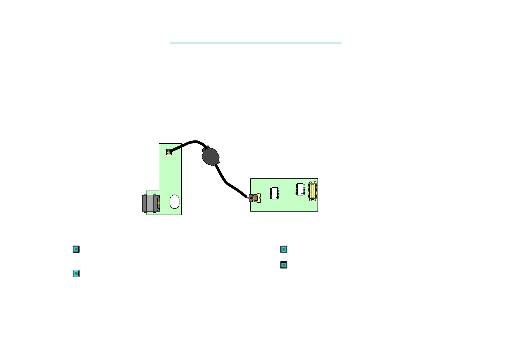
MDC/LAN transfer board
J21
J1
J1: RJ-11 phone jack for internal
modem.
J21: MDC jump wire connector.
JP1
U2
U1
JP3
JP1: MDC jump wire connector.
JP3: Connector for MDC/LAN
transfer board to M/B.
77
Page 79
7321 N/B Maintenance7321 N/B Maintenance
3. Definition & Location Of Connectors/switches
3.4 Charge Board
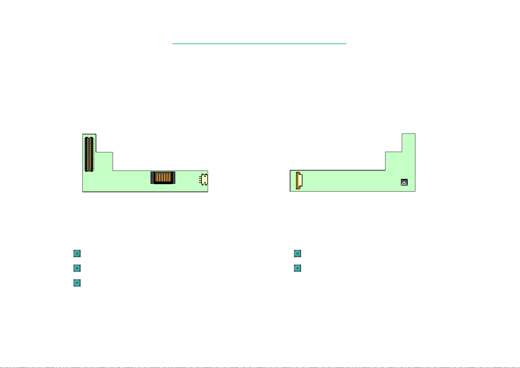
J1
J1: Charger & Touch-Pad connector to M/B.
J2: Internal speaker connector.
PJ4: Battery pack connector.
Charge board(side A)
PJ4
J2
Charge board(side B)
SW500
J500
J500: Touch-Pad button connector.
SW500: CMOS Reset
78
Page 80

7321 N/B Maintenance7321 N/B Maintenance
4. Definition & Location Of Major Components
4.1 Main Board ( Side a )
U1
U3
U10
U30
U6
U24
U1: ADM3311ARU RS232/SIO.
U3: TPA0202 AUDIO AMP
U5: LANPHY LSIL80227
U6: CH7005C(TV Encode).
U5
U14
U27
U21
U15
U22
U25
U28
U10: CS4299 AC’97 CODE
U14: Power switch matrix(PC CARD)
U21: North Bridge VT8362
U24: South Bridge VT8231
U8
U16
U23
U26
U29
U30: H8(3434F,KB BIOS)
U15,U22,U25,U28
U16,U23,U26,U29:
On board SDAM.
U8: ICS9248-102(Clock generator
U27: System BIOS.
79
Page 81

7321 N/B Maintenance7321 N/B Maintenance
4. Definition & Location Of Major Components
4.2 Main Board ( Side b )
U502
U503
U504
U502: PH163112 LAN Controller.
U503: Socket A CPU.
U504: PCI1225PDV PC CARD interface controller.
80
Page 82

7321 N/B Maintenance7321 N/B Maintenance
5. Pin Descriptions of Major Components
5.1 Mobile AMD K7 Processor
Mobile AMD Athlon™ H- series OBGA Processor Model 6 Ball Diagram-Bottomside View
81
Page 83
7321 N/B Maintenance7321 N/B Maintenance
5. Pin Descriptions of Major Components
5.1 Mobile AMD K7 Processor
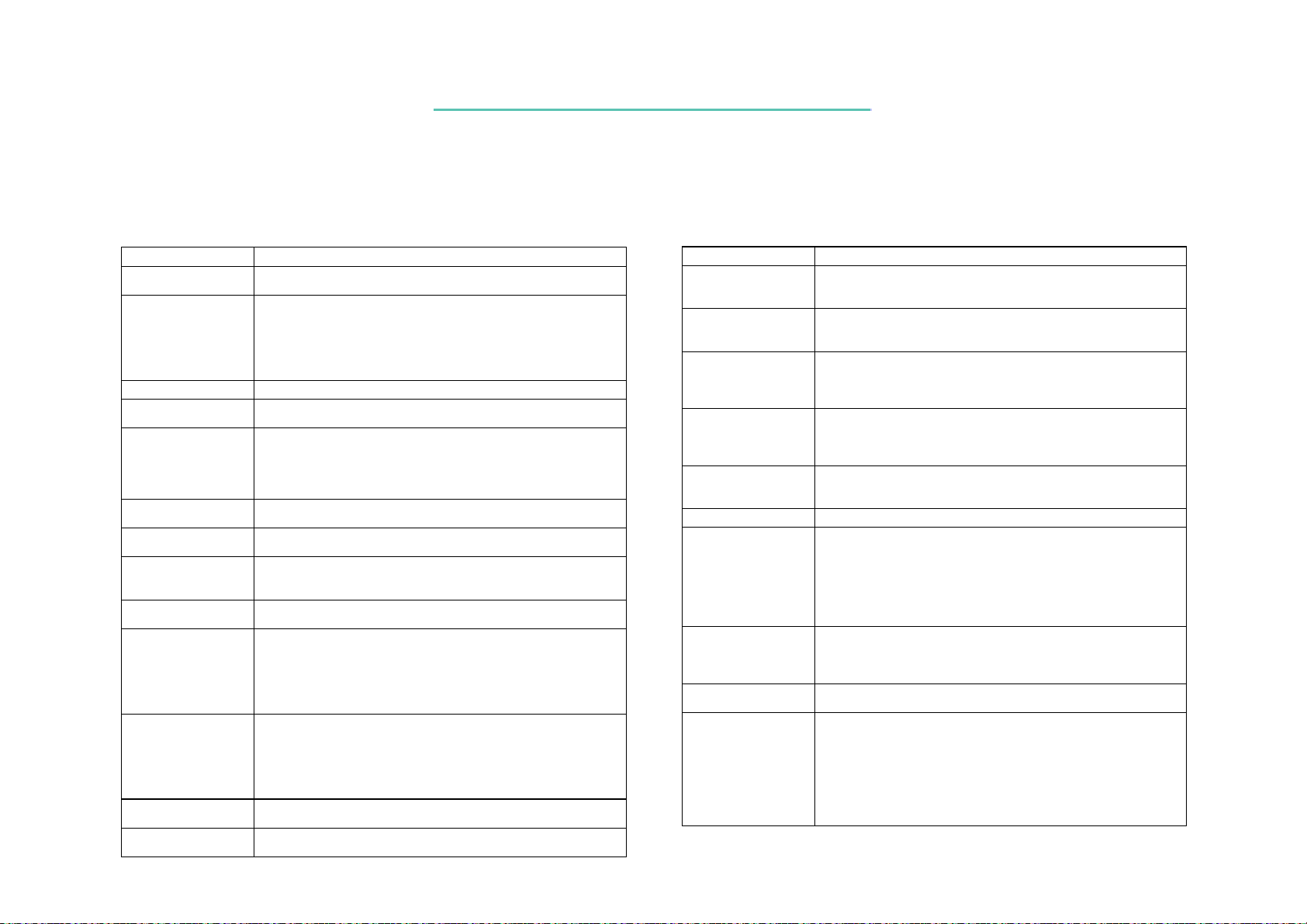
Detailed Ball Descriptions
A20M# Ball
AMD Athlon™
Processor System B us
Balls
Analog Ball
CLKFWDRST Ball
CLKIN and RSTCLK
(SYSCLK) Balls
CONNECT Ball
COREFB and
COREFB# Balls
CPU_PRESENCE#
Ball
DBRDY and DBREQ#
Balls
FERR Ball
FID[3:0] Balls
FLUSH# Ball
IGNNE# Ball
Name Description
A20M# is an input from the system used to sim ulate address wr ap-ar ound
in the 20-bit 8086.
See the AMD Athlon™ and AMD Duron™ Processor System Bus
Specification, order# 21902 for information about the system bus
balls —PROCRDY, PWROK, RESET #, SADDIN[14:2]#,
SADDINCLK#, SADDOUT[14:2]#, SADDOUTCLK#, SCHECK[7:0]#,
SDATA[63:0]#, SDATAINCLK[3:0]#, SDATAINVALID#,
SDATAOUTCLK[3:0]#, SDATAOUTVALID#, SFIL L VAL ID# .
Treat this ball as a NC.
CLKFWDRST resets clock-forward circuitry for both the system and
processor.
Connect CLKIN (AC16) with RSTCLK (AC17) and name it SYSCLK.
Connect CLKIN# (AD16) with RSTCLK# (AD17) and name it
SYSCLK#. Length match the clocks from the clock generator to the
Northbridge and processor.
See “SYSCLK and SYSCLK#”, for more informati on.
CONNECT is an input from the system used for power management and
clock-forward initialization at reset.
COREFB and COREFB# are outputs to the system that provide pr ocess or
core voltage feedback to the system.
CPU_PRESENCE# is connected to VSS on the processor package. If
pulled-up on the motherboard, CPU_PRESENCE# may be used to detect
the presence or absence of a processor.
DBRDY (AB2) and DBREQ# (T4) are routed to the debug connector.
DBREQ# is tied to VCC_CORE with a pullup resistor.
FERR is an output to the system that is asserted for any unmasked
numerical exception independent of the NE bit in CR0. FERR is an
open-drain active High signal that must be inver ted and level shifted to an
active Low signal. For more information about FERR and FERR#, see
the “Required Circuits” chapter of the AMD Athlon™ Processor
Motherboard Design Guide, order# 24363.
The FID[3:0] balls drive a value of: FID[3:0] = 0 1 0 0
that corresponds to a 5x SYSCLK multiplier after PWROK is asserted to
the processor. This information is used by the Northbridge to create the
SIP stream that the Northbridge sends to the processor after RESET# is
deasserted.
For more information, see “SYSCLK Mult i pliers”.
FLUSH# must be tied to VCC_CORE with a pullup resistor. If a debug
connector is implemented, FLUSH# is routed to the debug connector.
IGNNE# is an input from the system that tells the processor to ignore
numeric erro rs.
INIT# Ball
INTR Ball
JTAG Balls
K7CLKOUT and
K7CLKOUT# Balls
NC Balls
NMI Ball
PLL Bypass and Test
Balls
PWROK Ball
RSVD Balls
SADDIN[1:0]# and
SADDOUT[1:0]# Balls
Name Description
INIT# is an input from the system that resets the integer registers without
affecting the floating-point registers or the internal caches. Execution
starts at 0FFFF FFF0h.
INTR is an input from the system that causes the processor to start an
interrupt acknowledge transaction that fetches the 8-bit interrupt vector
and starts execution at that location.
TCK (V1), TMS (K3), TDI (W2), TRST# (Y1), and TDO (Y2) are the
JTAG interface. Connect these balls directly to the motherboard debug
connector. Pullup TDI, TCK, TMS, and TRST# to VCC_CORE with
pullup resistors.
K7CLKOUT (AC19) and K7CLKOUT# (AD19) are each run for 2 to 3
inches and then terminated with a resistor pair, 100 o hms to V CC_CO RE
and 100 ohms to VSS. The effective termination resistance and voltage
are 50 ohms and VCC_CORE/2.
The motherboard should provide a surface mount pad for all 564 package
balls. The pads for NC balls should not be electrically connected to
anything.
NMI is an input from the system that causes a non-maskable interrupt.
PLLTEST# (AA3), PLLBYPASS# (AB23), PLLMON1 (AD13),
PLLMON2 (AC13), PLLBYPASSCLK (AB17), and PLLBYPASSCLK#
(AB16) are the PLL bypass and test interface. This interface is tied
disabled on the motherboard. All six ball signals are routed to the debug
connector. All four processor inputs (PLLTEST#, PLLBYPASS#,
PLLMON1, and PLLMON2) are tied to VCC_CORE with pullup
resistors.
The PWROK input to the processor must not be asserted until all voltage
planes in the system are within specification and all system clocks are
running within specification.
For more infor mation, s ee “Signal and Power -Up Requirements”.
Reserved balls must have pulldown resistors to ground on the
motherboards.
The mobile AMD Athlon H-series OBGA processor model 6 does not
support SADDIN[1:0]# or SADDOUT[1:0]#. SADDIN[1]# is tie d to
VCC_CORE with pullup resistors, if this bit is not supported by the
Northbridge (future models of the AMD Athlon processors may support
SADDIN[1] #) . SADDOUT[1:0]# are tied to VCC_CORE with pullup
resistors if these balls are supported by the Northbridge. For more
information, see the AMD Athlon™ and AMD Duron™ Processor
System Bus Specification, order# 21902.
82
Page 84
7321 N/B Maintenance7321 N/B Maintenance
p
5. Pin Descriptions of Major Components
5.1 Mobile AMD K7 Processor
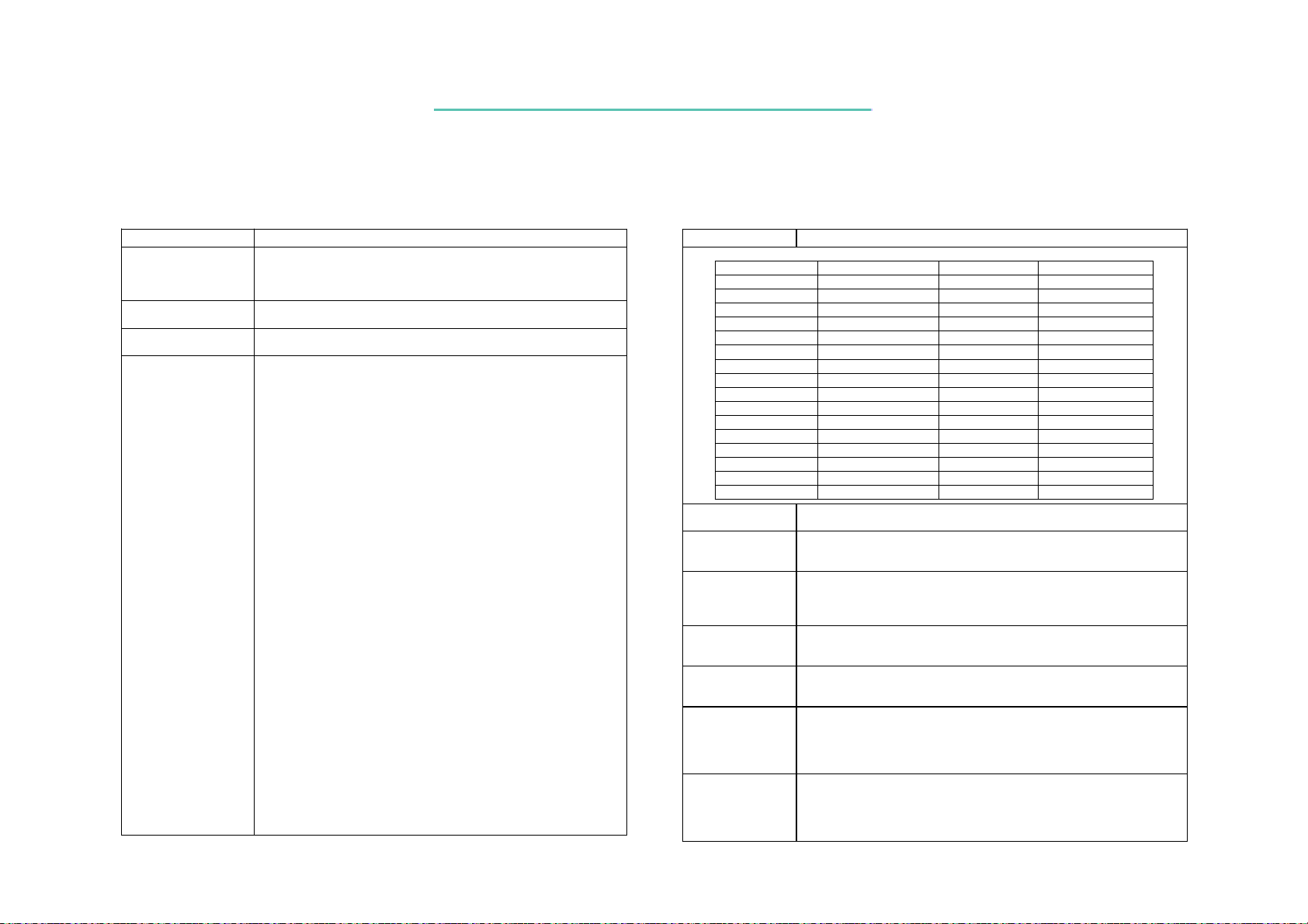
Name Description
Scan Ba lls
SCHECK[7:0]# Ball
SMI# B a ll
SOFTVID[4:0] and
VID[4:0] Balls
SCANSHIFTEN (L3), SCANCLK1 (W1), SCANINTEVAL (K4), and
SCANCLK2 (AA1) are the scan interface. This interface is AMD internal
and is tied disabled with pulldown resistors to ground on the
motherboard.
For systems that do not support ECC, SCHECK[7:0]# should be treated
as NC balls.
SMI# is an input that causes the processor to enter the system
management mode.
The VID[4:0] (Voltage ID) and SOFTVID[4:0] (Software driven
Voltage ID) outputs are used by the DC to DC power converter to select
the processor core voltage. The VID[4:0] balls are strapped to ground or
left unconnected on the package and must be pulled up on the
motherboard. The SOFTVID[4:0] balls are open drain and 2.5–V
tolerant. The SOFTVID[4:0] balls of the processor must not be pulled to
voltages higher than 2.5 V.
The moth erb o ard is req u ired to im p lement a VID multip lex e r to se lec t a
deterministic voltage for the processor at power–up before the PWROK
input is asserted. B e fore PWROK is asserted, th e VID multiplexer drives
the VID value from VID[4:0] balls to the DC to DC converter for
VCC_C O R E . A fter PWROK is asserted , th e V ID m ultip lex e r driv es th e
VID value from the SOFTVID[4:0] balls to the DC to DC converter for
VCC_ C ORE of the p ro ce ss o r. R e fe r to th e AM D Athlon™ Processor
Motherboard Design Guide, order# 24363 for the recommended VID
multiplexer c ircu it.
The SOFTVID[4:0] balls are driven by the processor to select the
maximum VCC_CORE of the processor as reported by the Maximum
VID field of the FidVidStatus MSR within 20 ns of PWROK assertion.
Bef ore PWROK i s asser t ed, the SOFTVID[4:0] outputs are not driven
to a deterministic value. The SOFTVID[4:0] outputs must be used to
select VCC _ C O R E a fter PWROK is asserted. A n y tim e th e R E SE T #
input is asserted, th e SO F TV ID [4 :0] b a lls will b e drive n to sele ct th e
maximum voltage.
Note: the Start–up VID and Maximum VID fields of the FidVidStatus
MSR report the same value that corresponds to the nominal voltage that
the processor requires to operate at maximum frequency.
AMD PowerNow!™ technology can use the FID_Change protocol
described in Section 4.1 on page 9 to transition the SOFTVID[4:0]
outputs and therefore VCC_CORE as part of processor performance state
transitions.
The VID codes used by the mobile AMD Athlon H-series OBGA
rocess or model 6 are defined in Table 23, “SOFTVID[4:0] and VID[4:0]
Code to Voltage Definition,” on page 81.
VID code s for Mobile AMD A th lo n p ro c esso rs are diffe ren t fro m
Note:
the VID codes for desktop AMD Athlon processors.
SOFTVID[4:0] and VID[4:0] Code to Voltage Definition
STPCLK# Ball
SYSCLK and
SYSCLK#
THERMDA and
THERMDC Balls
VCCA
VCCA_CAP1 and
VCCA_CAP2 Balls
VREF_SYS Ba ll
ZN and ZP Balls
Name Description
VID[4:0] (V)
00000 2.000 10000 1.275
00001 1.950 10001 1.250
00010 1.900 10010 1.225
00011 1.850 10011 1.200
00100 1.800 10100 1.175
00101 1.750 10101 1.150
00110 1.700 10110 1.125
00111 1.650 10111 1.100
01000 1.600 11000 1.075
01001 1.550 11001 1.050
01010 1.500 11010 1.025
01011 1.450 11011 1.000
01100 1.400 11100 0.975
01101 1.350 11101 0.950
01110 1.300 11110 0.925
01111 Shutdown 11111 Shutdown
VCC_CORE
STPCLK# is an input that causes the processor to enter a lower power mode
and issue a Stop Grant special cycle.
SYSCLK and SYSCLK# are differential input clock signals provided to the
PLL of the processor from a system-clock generator. See “CLKIN and
RSTC LK (SYSCLK) Balls” , fo r m o re information .
Thermal Diode anode (THERMDA) and cathode (THERMDC) ball s are used
to monitor the actual temperature of the processor die, providing more
accurate temperature control to the system. See Table 17, “Thermal Diod e
Characteristic s”, fo r m o re d etails.
VCCA is the processor PLL supply. For information about the VCCA balls,
see Table 7, “VCCA AC and DC C haracteristics,” and the AMD Athlon™
Processor Motherboard Design Guide, order# 24363.
The motherboard must connect VCCA_CAP1 and VCCA_CAP2 balls to
VSS with a capacitor. Refer to AMD Athlon™ Processor Motherboard
Design Guide, order# 24363 for population details.
VREF_SYS (W3) drives the threshold voltage for the system bus input
receivers. The value of VRE F_SY S is sy stem specific. In additio n , to
minimize VCC_CORE noise rejection from VREF_SYS, i ncl ude decoupl i
ng capaci tors. For more information, see the AMD Athlon™ Processor
Motherboard Design Guide, order# 24363.
ZN (Y4) and ZP (AC4) are the push-pull compensation circuit balls. In
Push-Pull mode (selected by the SIP parameter SysPushPull asserted), ZN is
tied to VC C _ C O R E w ith a resisto r tha t h as a resistan c e m a tch in g th e
impedan c e Z 0 o f the tran sm ission lin e. Z P is tied to V SS w ith a resisto r tha t
has a resistance matching the impedance Z 0 of the transmission line.
VID[4:0]
VCC_CORE (V)
83
Page 85
7321 N/B Maintenance7321 N/B Maintenance
10=8, 11=8. 5, 1 2=9,
5. Pin Descriptions of Major Components
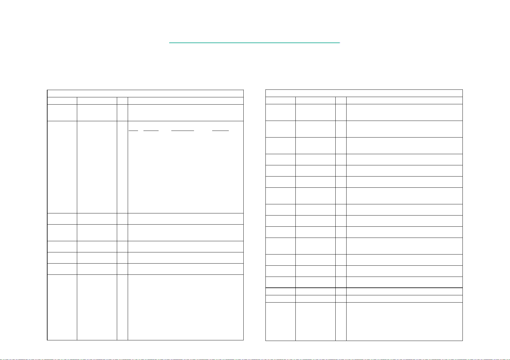
5.2 VIA VT8362 North Bridge with S3 Savage4 AGPX4
DRAM Interface
Signal Name PIN # I/O Signal Description
MD[63:0]
MA14/ strap,
MA13/ strap,
MA12/ strap,
MA11/ strap,
MA10/ strap,
MA9/ strap,
MA8/ strap,
MA7/ strap,
MA6/ strap,
MA5/ strap,
MA4/ strap,
MA3/ strap,
MA2/ strap,
MA1/ strap,
MA0/ strap
CS[5:0]#
DQM[7:0]
SRASA#/
strap
SCASA# /
strap
SWEA# /
strap
CKE0 /
SWEC#,
CKE1 /
SCASC#,
CKE2 /
SWEB#,
CKE3 /
SCASB#,
CKE4 /
SRASC#,
CKE5 /
SRASB#
(see pinout tables) IO Memory Data. These signals are connected to the DRAM
W22
W23
W24
W25
W26
V24
V25
U21
V22
U22
V23
T22
V26
U23
U24
Y23, Y22, AA25,
AA26, Y26, Y25
R24, T26, AA24,
AB26, R26, R23,
AA22, AA23
U25 O Row Address Command Indicator. (strap at Device 0
P25 O Column Address Command Indicator. (strap at Device
AB24 O Write Enable Command Indicator. (strap at Device 0
U26
T25
P26
R25
AC26
AB25
data bus. Output drive strength may be set by Device 0
Rx6D[4].
O/ I Memory Address. DRAM address lines
St r ap
St r ap Register
Re g i s t e r Des cr i pt i on
St r apSt r ap
Re g i s t e rRe g i s t e r
MA1 4 Rx68[0] CPU Cl oc k Fr eque ncy 0=100, 1=133
MA1 3- 12 RxB4[7-6] Dri ve Strengt h for Rise 11=Aut o, ~11=St r a p
MA11 RxB6[7] S2K Edge/Central DQ 0=Central, 1=Edge
MA1 0-9 RxB4[3-2] Drive Strength for Fall 0=Auto, ~0=St rap
MA8 - 4 Rx B6 [ 5 - 1] S2K Strobe Delay 0=Auto, ~0=Strap
MA3-0 RxB3[6-3] CPU Clock Divide 0=11, 1=11.5, 2=12,
3=12. 5, 4=5, 5=5. 5,
6=6,7=6.5,8=7,9=7.5,
13=9. 5, 14=10, 15=10. 5
SRASA# RxB2[5] S2K Slew Rate Control 0=Enable, 1=Disable
S CAS A# Rx B 3 [ 1] Fast Command 0=Disable, 1=Enabl e
SWEA# RxB6[6] CPU Edge/ Cent e r DQ 0=Edge, 1=Cen t er
Strap option default values are all 0 (internally pulled
down) MA output drive strength may be set by Device 0
Rx6C[7] and 6D[2]. Cmd output drive strength may be set
by Device 0 Rx6C[6] and 6D[3].
O Chip Select. Chip select of each bank. Output drive
strength may be set by Device 0 Rx6D[0].
O Data Mask. Data mask of each byte lane. Output drive
strength may be set by Device 0 Rx6D[1].
RxB2[5])
0 RxB3[1])
RxB6[6])
O Clock Enables. Clock enables for each DRAM bank for
powering down the SDRAM or clock control for reducing
power usage and for reducing heat / temperature in
high-speed memory systems. See Device 0 Rx78[0] and
RxE0[4].
Des cr i pt i on Settings
Des cr i pt i on Des cr i pt i on
Settings
Settings Settings
Signal Name PIN # I/O Signal Description
AD[31:0]
CBE[3:0]#
FRAME#
IRDY#
TRDY#
STOP#
DEVSEL#
PAR
SERR#
LOCK#
PREQ#
PGNT#
REQ[4:0]#
GNT[4:0]#
PCLK
PCKRUN#
INTA#
(see pinout tables) IO
AC10, AB12,
AF14, AE15
AC12 IO
AF12 IO
AE12 IO
AB13 IO
AD12 IO
AE13 IO
AF13 IO
AC13 IO
AE18 I
AF18 O
AB8, AC6, AC7,
AE6, AE7
AB7, AD6, AD7,
AF6, AF7
AB18 I
AC17 IO
AB6 O
IO
PCI Bus Interface
Address/Data Bus.
lines. The address is driven with FRAME# assertion an d
data is driven or received in following cycles.
Command/Byte Enable.
FRAME# assertion. Byte enables corresponding to
supplied or requested data are driven on following clocks.
Assertion indicates the address phase of a PCI
Frame.
transfer. Negation indicates that one more data transfer is
desired by the cycle initiator.
Initiator Ready.
data transfer.
Target Ready.
transfer.
Asserted by the target to request the master to stop
Stop.
the current transaction.
Device Select.
PCI initiator is attempting to access main memory. It is an
input when the VT8362 is acting as a PCI initiator.
A single parity bit is provided over AD[31:0] and
Parity.
C/BE[3:0].
System Error.
detects a system error condition.
Lock.
lock.
South Bridge Request.
Bridge. PREQ# is the South Bridge request for the PCI
bus.
South Bridge Grant.
grant PCI access to the South Bridge.
I
PCI Master Request.
O
PCI Master Grant.
use PCI.
PCI Clock.
PCI Clock Run.
PCI Interrupt Out.
used to signal an event that requires handling on behalf of
the internal integrated graphics controller. If MA2 is
strapped high at reset (clearing CR36[0]) no interrupt will
be requested during PCI configuration. The default drive
strength is 24 mA (other drive strengths may be selected
via CR80[1-0]).
Used to establish, maintain, and release resource
The standard PCI address and data
Commands are driven with
Asserted when the initiator is ready for
Asserted when the target is ready for data
This signal is driven by the VT8362 w hen a
The VT8362 will pulse this signal when it
This signal comes from the South
This signal driven by the VT8362 to
PCI master requ e st s for PCI.
Permission is given to the master to
From external clock generator.
May be used to stop PCI clock.
An asynchronous active low output
84
Page 86
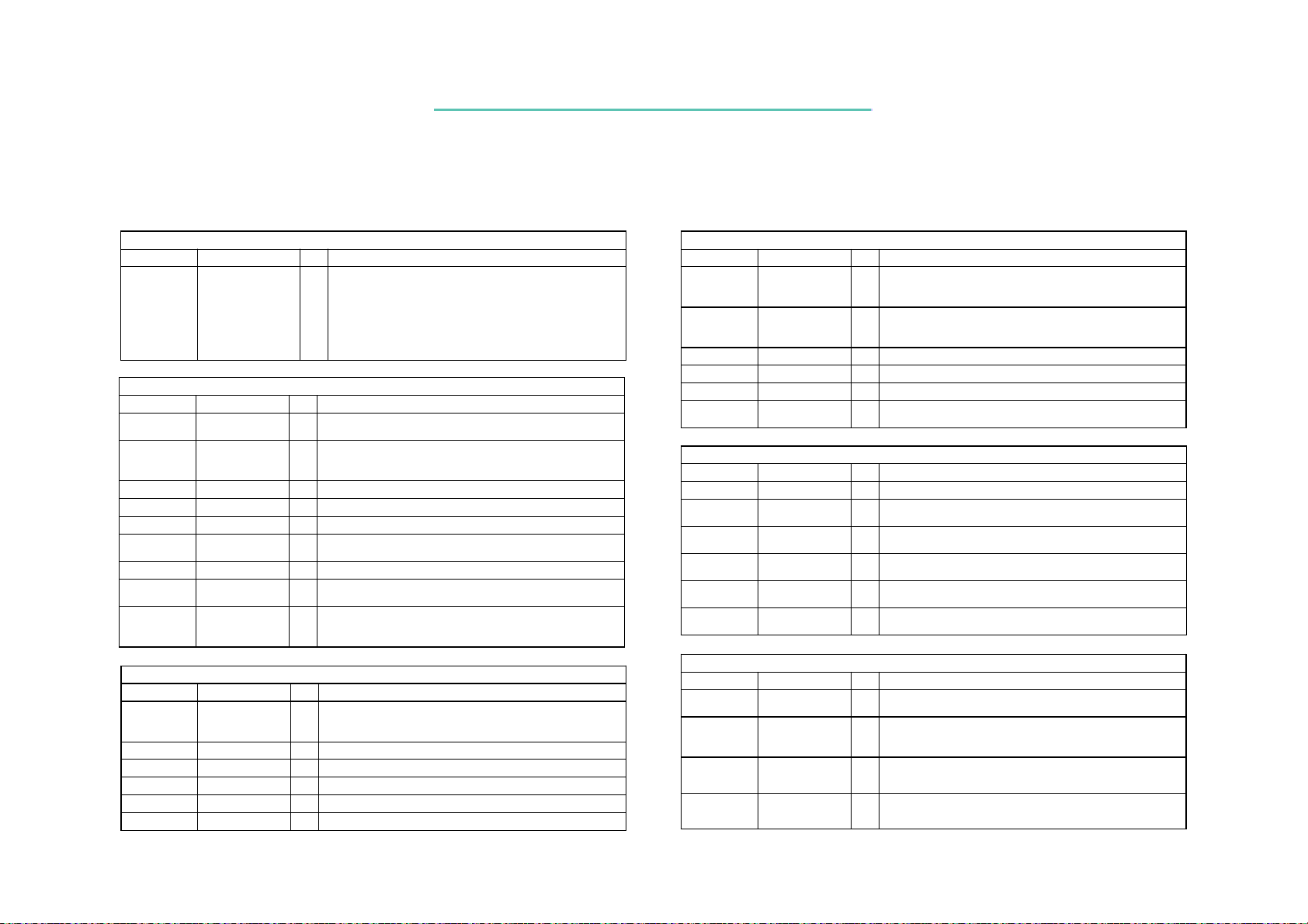
7321 N/B Maintenance7321 N/B Maintenance
5. Pin Descriptions of Major Components
5.2 VIA VT8362 North Bridge with S3 Savage4 AGPX4
PCI Bus Inter face
Signal Name PIN # I/O Signal Description
WSC#
Signal Name PIN # I/O Signal Description
FPD[35:0]
FPDET
FPVS
FPHS
FPDE
FPCLK
FPGPIO
ENVDD
ENVEE
AC18 O
(see pin table) O
AA7 I
G3 O
G5 O
H3 O
G4 O
G1 I/O
F1 O
H5 O
Write Snoop Complete.
planar on ly in m u ltip roc esso r co n figu ratio n s) asse rted to
indicate that all snoop activity on the CPU bus initiated by
the last PCI-to-DRAM write is co m p le te a n d th a t it is safe
to send an A P IC in terrup t message. Basically th is sign al is
always active except when PCI master write data is not
flushed.
LCD Panel Interface
Panel Data.
default. 16mA is selected via SR3D[6]=1.
Panel Detect.
Panel is a ppropriately connected. Must be tied to GND if not
used.
Panel VSYNC.
Panel HSYNC.
Panel D a ta Enable.
Panel Clock.
the default. 16mA may also be selected.
General Purpose Input/Output.
Enable VDD.
initiate a flat pa ne l p o w er u p seq u en c e.
Enable VEE.
time after ENVDD is driven high during a flat panel power
up sequence.
Internally pulled down during reset. 8mA is the
If SR30[1 ]=0 , S R 3 0 [2 ] will re ad 1 if a F la t
Internally pulled down.
Internally pulled down.
Internally pulled down during reset. 8mA is
This signa l is driv e n h ig h to ex te rna l lo g ic to
This signal is driven high to a programmable
CRT Interface
Signal Name PIN # I/O Signal Description
RSET
AR
AB
AG
HSYNC
VSYNC
C1 A
C2 A
B2 A
B1 A
F5 O
F4 O
Reference Resistor.
140??resistor to control
the RAMDAC full-scale current value.
Analog Red.
Analog Blue.
Analog Green.
Horizontal Sync.
Vertical Sync.
Analog red output to the CRT monitor.
Analog blue output to the CRT monitor.
Analog green output to the CRT monitor.
Output to CRT.
Sideband PCI signal (used on the
Internally pulled down.
Tie to GNDRGB through an external
Output to CRT.
FPD[11:0]
FPDET
FPVS
FPHS
FPDE
FPCLK
TVD[11:0]
TVCLK
FPD32
TVCLKR
FPD16
TVVS
FPD31
TVHS
FPD34
TVBL#
FPD17
Y[2:0]P
Y[2:0]M
YCP
YCM
Z[2:0]P
Z[2:0]M
ZCP
ZCM
Flat Panel Monitor (DVI) Interface
Signal Name PIN # I/O Signal Description
(see pin table) O
AA7 I
G3 O
G5 O
H3 O
G4 O
Signal Name PIN # I/O Signal Description
(see pin table) O
/
/
/
/
/
Signal Name PIN # I/O Signal Description
N5 I
K5 O
R4 O
R5 O
L1 O
AC2, AD3, AD1
AC1, AD2, AD4AA
AB4
AA5
AA4, AB2, AB3
A3, AB1, AC3AA
AA1
AA2
Panel Data.
default. 16mA is selected via SR3D[6]=1. This function is
selected on these pins when SR31[4] = 1.
Panel Detect.
Panel is a ppropriately c onne c ted. Must be tied to GND if not
used.
Panel VSYNC.
Panel HSYNC.
Panel D a ta E na b le.
Panel Clock.
the default. 16mA may also be selected.
TV Encoder Interface
TV D a ta .
TV Clock.
down.
TV Return Clock.
pulled down.
TV VSYNC.
TV HSYNC.
TV Blanking.
LVDS Interface
LVDS Data Positive Output.
LVDS Data Negative Output.
A
LVDS Clock Positive Output.
A
LVDS Clock Negative Output.
2 nd LVDS D a ta P o sitiv e O u tp u t.
2 nd LVDS Data Negative Output.
A
2 nd LVDS Clock Positive Output.
A
2 nd LVDS Clock Negative Output.
Internally pulled down during reset. 8mA is the
If SR30[1 ]=0 , S R 3 0 [2 ] w ill read 1 if a Fla t
Internally pulled down.
Internally pulled down.
Internally pulled down.
Internally pulled down during reset. 8mA is
Internally pulled down during reset
Input clock from encoder. Internally pulled
Output clock to TV encoder. Internally
Internally pulled down during reset
Internally pulled down during reset
Internally pulled down during reset
85
Page 87
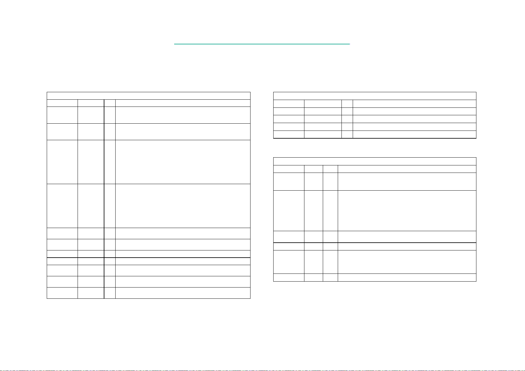
7321 N/B Maintenance7321 N/B Maintenance
5. Pin Descriptions of Major Components
5.2 VIA VT8362 North Bridge with S3 Savage4 AGPX4
Miscellaneous Functions
Signal Name PIN # I/O Signal Description
XIN
XOUT
SPCLK[2:1]
SPDAT[2:1]
STRW /
GPOUT
GOP0
STPAGP#
AGPBUSY#
STANDBY
SUSPEND
SUSST#
E1 I
E2 O
M2, AE5 IO
M3, AD5 IO
AE2 O
AF2 O
AE3 I
AD4 I/O
AE4 I
AC5 I
AB19 I
Reference Frequency Input.
connected between XOUT and this pin. Alternatively, an external
oscillator can b e connec ted.
Crystal O utput.
oscillator. If an externa l o scilla tor is co n n ec ted to X IN, th is p in
can be left unconnected.
Serial Port Clocks.
SPCLK1 is typically used for I²C communications. As an output,
it is programmed via CRA0[0]. As an input, its status is read via
CRA0[2]. In either case the serial port must be enabled by
CRA0[4] = 1. SPCLK2 is typically used for DDC monitor
communicatio ns . As an output, it i s programmed via CRB1[0 ]. As
an input, its status is read via CRB1[2]. The port is enabled via
CRB1[4] = 1.
Serial Port Data.
transfer. SPDAT1 is typically used for I²C communications. As an
output, it is programmed via CRA0[1]. As an input, its status is
read via CRA0[3]. In either case the serial port must be enabled
by CRA0[4] = 1. SPDAT2 is typically used for DDC monitor
communicatio ns . As an output, it i s programmed via CRB1[1 ]. As
an input, its status is read via CRB1[3]. The port is enabled via
CRB1[4] = 1.
General Purpose Output.
General Output Port.
the state of CR5C[0].
Stop AGP.
AGP Busy.
Standby.
standby state.
Suspend.
suspend sta te.
Suspend Status.
feature. Connect to an external pullup to disable.
This pin driv es th e c rystal v ia an internal
These are the clocks for serial data transfer.
These are the data signals used for serial data
Power ma nagement fo r internal AGP .
Power ma nagement fo r i n te rn a l A G P .
Used to pu t th e in teg rate d g rap h ics c o n tro ller in th e
Used to pu t th e in teg rate d g rap h ics c o nt ro ller in th e
For implemen tatio n o f the Su spend-to-DRAM
An external 14.318 MHz crystal is
This pin reflects the state of SRD[0].
When SR1A[4] is cleared, this pin reflects
ZV-Port Interface
Signal Name PIN # I/O Signal Description
ZVD[15:0]
ZVHS
ZVVS
ZVCLK
(see pin table) I
V3 I
V1 I
W3 I
ZV-Port Data Bus Video Input.
ZV-Port Horizontal Sync.
ZV-Port Vertical Sync.
ZV-Port Clock.
Clock / Reset Control
Signal Name PIN # I/O Signal Description
HCLK
PCLK
MCLK
MCLKF
RESET#
PWROK
G22 I
AB18 I
R22 O
P23 I
AD18 I
AC19 I
Host Clock.
MHz). This clock is used by all TwisterK logic that is in the host
CPU domain.
PCI Clock.
create 33 MHz. This clock is used by all of the TwisterK logic that
is in the PCI clock domain. This clock input must be 33 MHz
maximum to comply with PCI specification requirements and must
be synchronous with the host CPU clock, HCLK, with an
HCLK:PCLK frequency ratio of 3:1. The hos t CP U clock mus t lead
the PCI clock by 2.0 ± 1.0 nsec.
DRAM Clock.
clock buffer.
DRAM Clock Feedback.
Reset.
resets TwisterK and sets all register bits to the default value. The
rising edge of this signal is used to sample all power-up strap
options
Power OK.
This pin receives the host CPU clock (66 / 100 / 133
This pin receives a buffered host clock divided-by-3 to
Output from internal clock generator to the external
Input from the external clock buffer.
Input from South Bridge chip. When asserted, this signal
Connect to South Bridge and Power Good circuitry.
86
Page 88

7321 N/B Maintenance7321 N/B Maintenance
b
5. Pin Descriptions of Major Components
5.3 VIA VT8231 BGA PCI-LPC/ISA South Bridge
PCI Bus Interface
Signal Name PIN # I/O Signal Description
AD[31:0]
C/BE[3:0]#
FRAME#
IRDY#
TRDY#
STOP#
DEVSEL#
PAR
SERR#
PINTA-D#
PCICLK
(see pin list) IO
C5, D6,
A8, F10
F6 IO
C7 IO
B7 IO
D7 IO
A7 IO
C8 IO
E7 I
B2, B1,
C3, C2
M17 I
IO
Address/Data Bus.
The address is driven with FRAME# assertion and data is
driven or received in following cycles. IDSEL is internally
connected to AD28.
Command/Byte Enable.
FRAME# assertion. Byte enables corre sponding to supplie d or
requested data are driven on following clocks.
Assertion indicates the address phase of a PCI
Frame.
transfer. Negation indicates that one more data transfer is
desired by the cycle initiator.
Initiator Ready.
transfer.
Target Ready.
transfer.
Asserted by the target to request the master to stop the
Stop.
current transaction.
Device Select.
transactions through positive or subtractive decoding. As an
input, DEVSEL# indicates the response to a VT8231-initiated
transaction and is also sampled when decoding whether to
subtractively decode the cycle.
A single parity bit is provided over AD[31:0] and
Parity.
C/BE[3:0]#.
System Error.
device that detects a system error condition. Upon sampling
SERR# active, the VT8231 can be programmed to generate an
NMI to the CPU.
I
PCI Interrupt Request
the PCI bus INTA#-INTD# pins as follows:
PINTA#
PCI Slot 1 INTA# INTB# INTC# INTD#
PCI Slot 2 INTB# INTC# INTD# INTA#
PCI Slot 3 INTC# INTD# INTA# INTB#
PCI Slot 4 INTD# INTA# INTB# INTC#
PCI Slot 5 INTA# INTB# INTC# INTD#
PCI Clock.
PCI Bus.
The standard PCI address and data lines.
The command is driven with
Asserted when the initiator is ready for data
Asserted when the target is ready for data
The VT8231 asserts this signal to claim PCI
SERR# can be pulsed active by any PCI
. These pins are typically connected to
PINTB# PINTC# PINTD#
PCLK provides timing for all transactions on the
Signal Name PIN # I/O Signal Description
PCKRUN#
PCIRST#
PCISTP#
GPO6
CPUSTP#
GPO5
PREQH#
PGNTH#
PREQL#
PGNTL#
HREQ1#
GPI10
HGNT1#
GPO8
HREQ2#
GPI11
HGNT2#
GPO9
LREQ1#
GPI12
LGNT1#
GPO10
R5 IO
E4 O
/
/
/
/
/
/
/
/
T4 O
P4 O
C1 O
D3 I
D2 O
D1 I
Y11 I / IO
W11 O / IO
V11 I / IO
T10 O / IO
U10 I / IO
Y10 O / IO
PCI Bus Clock Run.
or will be stopped (high) or running (low). The VT8231 drives this
signal low when the PCI clock is running (default on reset) and
releases it when it stops the PCI clock. External devices may assert
this signal low to request that the PCI clock be restarted or prevent
it from stopping. Connect this pin to ground using a 100 Ω?resistor
if the function is not used. Refer to the “PCI Mobile Design Guide”
and the VIA “Apollo MVP4 Design Guide” for more details.
PCI Reset.
PCI Stop.
CPU Stop.
PCI Request.
request the PCI bus for high priority access. The internal LAN
requests the PCI bus using this signal, so if the LAN subsystem is
used, this signal must be connected (one of the H/LREQ/GNT 1 and
2 pairs provided
PCI slot if desired). If the LAN subsystem is not used, PREQH# /
PGNTH# may optionally remain unconnected.
PCI Grant.
signal to grant high priority PCI access to the VT8231.
PCI Request.
request the PCI bus for normal priority access.
PCI Grant.
output to grant normal priority PCI access to the VT8231.
High Priority Request 1.
High Priority Grant 1.
High Priority Request 2.
High Priority Grant 2.
Low Priority Reque st 1 .
Low Priority Grant 1.
This signal is driven by the North Bridge GNT4#
This signal is driven by the North Bridge PGNT#
This signal indicates whether the PCI clock is
This signal goes to the North Bridge REQ4# input to
y the VT8231 may be used to implement the fifth
This signal goes to the North Bridge PREQ# input to
Device 0 Function 4 RxE5[3] = 0.
Device 0 Function 4 RxE5[3] = 0.
Device 0 Function 4 RxE5[3] = 0.
Device 0 Function 4 RxE5[3] = 0.
Device 0 Function 4 RxE5[2] = 0.
Device 0 Function 4 RxE5[2] = 0.
87
Page 89
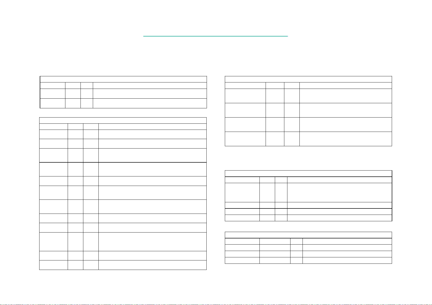
7321 N/B Maintenance7321 N/B Maintenance
5. Pin Descriptions of Major Components
5.3 VIA VT8231 BGA PCI-LPC/ISA South Bridge
PCI Bus Interface
Signal Name PIN # I/O Signal Description
/
/
W10 I / IO
V10 O / IO
Low Priority Request 2.
Low Priority Grant 2.
LREQ2#
GPI13
LGNT2#
GPO11
CPU Interface
Signal Name PIN # I/O Signal Description
CPURST
INTR
NMI
INIT
STPCLK#
SMI#
FERR#
IGNNE#
/ GPO7
SLP#
A20M#
DTD+
DTD-
Note: Connect each of the above signals to 4.7KΩ pullup resistors to VCC3
U4 OD
R6 OD
T5 OD
V5 OD
V6 OD
Y5 OD
U5 I
T6 OD
U6 OD
W5 OD
L2 Analog
L3 Analog
CPU Reset.
during power-up.
CPU Interrupt.
CPU that an interrupt request is pending and needs service.
Non-Maskable Interrupt.
non-maskable interrupt to the CPU. The VT8231 generates an
NMI when either SERR# or IOCHK# is asserted.
Initialization.
shut-down special cycle on the PCI bus or if a soft reset is
initiated by the register
Stop Clock.
throttle the processor clock.
System Management Interrupt.
VT8231 to the CPU in r es pons e to dif f er ent P ower - Managem ent
events.
Numerical Coprocessor Error.
coprocessor error signal on the CPU. Internally generates
interrupt 13 if active.
Ignore Numeric Error.
error” pin on the CPU.
Sleep
with slot-1 CPUs only. Not currently us ed with sock et-7 C PUs.
A20 Mask.
address bit-20 generation. Logical combination of the
A20GATE input (from internal o r e xternal keyboard controller)
and Port 92 bit-1 (Fast_A20). See Device 0 Function 0 Rx59[1].
CPU DTD (Thermal Diode) Channel Plus.
I
cathode of first external temperature sensing diode.
CPU DTD (Thermal Diode) Channel Minus.
I
anode of first external temperature sensing diode.
The VT8231 asserts CPURST to reset the CPU
STPCLK# is asserted by the VT8231 to the CPU to
(F4 RxE4[4] = 1). Used to pu t th e C PU to sle ep . Used
Connect to A20 mask input of the CPU to control
Device 0 Function 4 RxE5[2] = 0.
Device 0 Function 4 RxE5[2] = 0.
INTR is driven by the VT8231 to signal the
NMI is used to force a
The VT8231 asserts INIT if it detects a
SMI# is asserted by the
This signal is tied to the
This pin is connected to the “ignore
Connect to
Connect to
Strap
Strap
GPO17
Strap
Strap
Note: External strap option values may be set by connecting the indicated external pin to a 4.7K ohm
pullup (for 1 or H) or driving it low during reset with a 7407 TTL open collector buffer (for 0
or L) as shown in the suggested circuit below:
WSC#
APICD0
APICD1
APICCLK
LFRAME#
LDRQ#
LAD[3-0]
Note: For LPC control, see Device 0 Function 0 Rx58[5] and Rx59[4-3]
Note: Connect the LPC interface LPCRST# (LPC Reset) signal to PCIRST#
Strap Options
Signal Name PIN # I/O Signal Description
/ SUSA#/ GPO1 P1 I / O
/ MCCS#/
/ SA16
/ SA17
Advanced Programmable Interrupt Controller (APIC) Interface
Signal Name PIN # I/O Signal Description
/ GPI14
/ GPO28 W4 O / O
/ GPO29 Y4 O / O
/ GPI9 Y3 I / I
Signal Name PIN # I/O Signal Description
/ GPI15
W6 I / O
Y14 I / IO
T13 I / IO
V4 I / I
Low Pin Count (LPC) Interfac e
W8 O
Y8 I / I
V7, W7, Y7, V8 IO
CPURST / INIT Polarity
H: Slot-1 / Socket-370 / Slot-A / Socket-462
L: Socket-7
CPU Frequency Strappi ng
H: Disable
L: Enable
BIOS ROM Interface
H: LPC
L: Conventional
Auto Reboot
H: Disable (recommended)
L: Enable
Internal APIC Write Snoop Complete.
Asserted by the north bridge to indicate that all snoop activity
on the CPU bus initiated by the last PCI-to-DRAM write is
complete and that it is safe to perform an APIC interrupt.
Internal APIC Data 0.
Internal APIC Data 1.
APIC Clock.
LPC Frame.
LPC Data Request.
LPC Address / Data.
F0 Rx58[6] = 1.
F0 Rx58[6] = 1.
F0 Rx58[6] = 1.
F0 Rx58[6] = 1.
F0 Rx58[5] = 1.
88
Page 90

7321 N/B Maintenance7321 N/B Maintenance
5. Pin Descriptions of Major Components
5.3 VIA VT8231 BGA PCI-LPC/ISA South Bridge
LAN Controller - Media Independent Interface (MII)
Signal Name PIN # I/O Signal Description
MCOL
MCRS
MDCK
MDIO
MRXCLK
MRXD[3]
MRXD[2]
MRXD[1]
MRXD[0]
MRXDV
MRXERR
MTXCLK
MTXD[3]
MTXD[2]
MTXD[1]
MTXD[0]
MTXENA
The internal LAN controller uses the high priority PCI bus requ est / g rant p air (PREQH# / PGNTH#)
to request PCI bus access from the chipset north bridge.
,
,
,
,
,
,
Signal Name PIN # I/O Signal Description
EECS#
EECK
EEDO
EEDI
G17 I
G16 I
C20 O
D18 IO
C19 I
D19
D20
E18
E19
E20 I
F18 I
F17 I
G20
G19
G18
F20
F19 O
I
I
I
I
O
O
O
O
C18 O
E16 O
D17 O
E17 I
MII Collision Detect.
MII Carrier Sense.
media is active.
MII Management Data Clock.
timing re fe re nce for MDIO
MII Manageme nt Da ta I/O .
to the MDO bit.
MII Receive Clock.
PHY.
MII Receive Data.
external PHY synchronous with MRXCLK.
MII Receive Data Valid.
MII Receive Error.
decoding error.
MII Transmit Clock.
supplied by the PHY.
MII Transmit Data.
to MTXCLK.
MII Transmit Enable .
port to the PHY.
Serial EEPROM Interface
Serial EEPROM Chip Select.
Serial EEPROM Clock.
Serial EEPROM Data Output.
Serial EEPROM Data Input.
From the external PHY.
Asserted by the external PHY when the
Sent to the external PHY as a
Read from the MDI bit or written
2.5 or 25 MHz clock recovered by the
Parallel receive data lines driven by the
Asserted by the PHY when it detects a data
Always active 2.5 or 25 MHz clock
Parallel transmit data lines synchronized
Indicates transmit active from the MII
USBP0+
USBP0USBP1+
USBP1USBP2+
USBP2USBP3+
USBP3USBCLK
USBOC0#
USBOC1#
USBOC2#
/ GPI20/ GPO20
USBOC3#
/ GPI20/ GPO21
SMBCK1
SMBCK2
SMBDT1
SMBDT2
SMBALRT#
* Note: SMBus #2 is a slave-only device used to supply status for external Alert-On-LAN (AOL)
Universal Serial Bus Interface
Signal Name PIN # I/O Signal Description
B18 IO
A18 IO
B19 IO
A19 IO
B20 IO
A20 IO
C17 IO
B17 IO
C15 I
A17 I
D16 I
/ LA20
/ LA21
Signal Name PIN # I/O Signal Description
/ GPIO27 R1 IO / IO
/ GPIO26 R2 IO / IO
/ GPI7 T2 I / I
W13 I / IO
Y13 I / IO
System Managem ent B us (SM B ) Interfa ce (I²C B us)
R3 IO
T1 IO
USB Port 0 Data +
USB Port 0 Data USB Port 1 Data +
USB Port 1 Data USB Port 2 Data +
USB Port 2 Data USB Port 3 Data +
USB Port 3 Data USB Clock.
USB Port 0 Over Current Detect.
this input is low.
USB Port 1 Over Current Detect.
this input is low
USB Port 2 Over Current Detect.
/ I / O
this input is low. Device 0 Function 4 RxE4[6] = 0 and
Power Management I/O Rx4E[4] = 1.
USB Port 3 Over Current Detect.
/ I / O
this input is low. Device 0 Function 4 RxE4[6] = 0 and
Power Management I/O Rx4E[5] = 1.
SMB / I²C Channel 1 Clock.
SMB / I²C Channel 2 Clock†.
SMB / I ²C Channel 1 Data.
SMB / I²C Channel 2 Data†.
SMB Alert.
1) When the chip is enabled to allo w it, assertion gen erates
an IRQ or SMI interrupt or a power management resume
event. The same pin is used as General Purpose Input 6
whose value is reflected in Rx48[6] of function 4 I/O space
48MHz clock input for the USB interface
Port 0 is disabled if
Port 1 is disabled if
Port 2 is disabled if
Port 3 is disabled if
(System Management Bus I/O space Rx08[3] =
89
Page 91
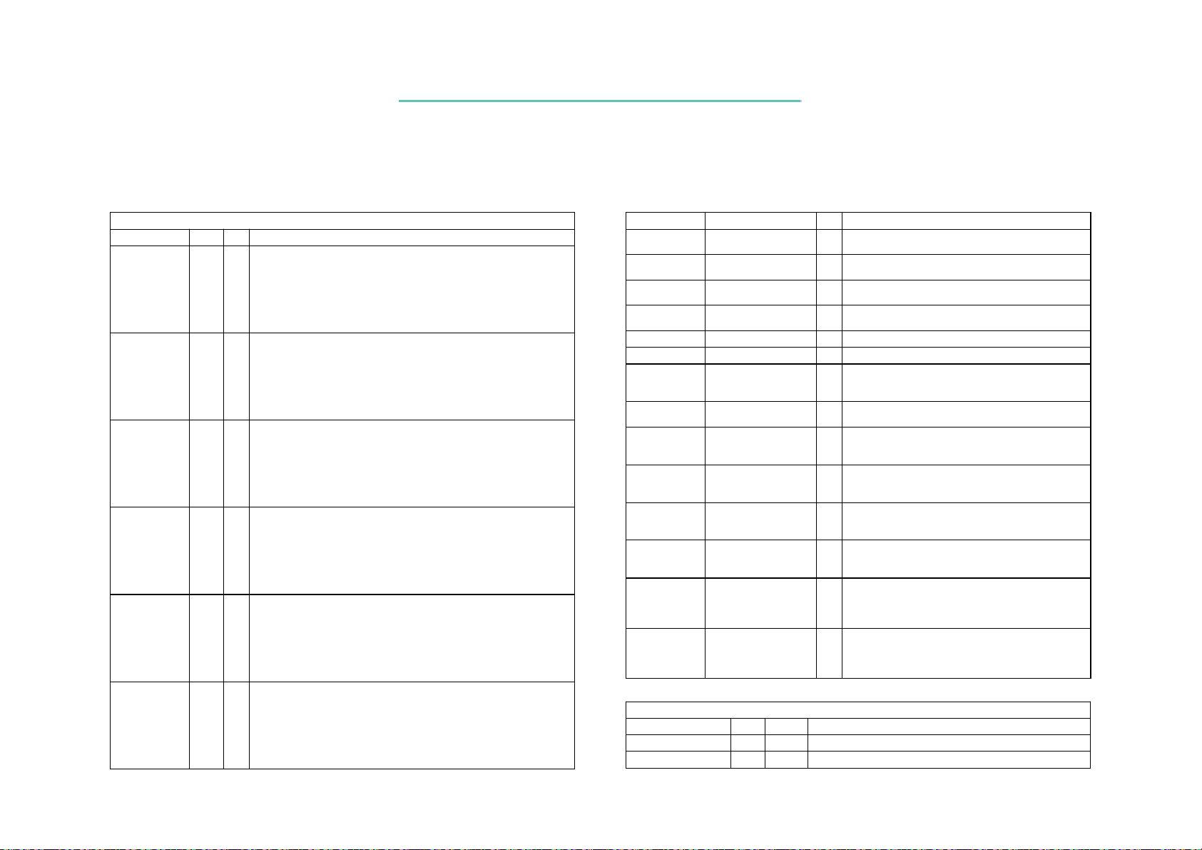
7321 N/B Maintenance7321 N/B Maintenance
5. Pin Descriptions of Major Components
5.3 VIA VT8231 BGA PCI-LPC/ISA South Bridge
UltraDMA-33 / 66 Enhanced IDE Interface
Signal Name PIN # I/O Signal Description
/
PDRDY
PDDMARDY/
PDSTROBE
/
SDRDY
SDDMARDY/
SDSTROBE
PDIOR#
PHDMARDY/
PHSTROBE
SDIOR#
SHDMARDY/
SHSTROBE
PDIOW#
PSTOP
SDIOW#
SSTOP
N19 I EIDE Mode:
Y20 I EIDE Mode:
/
N18 O EIDE Mode:
/
W19 O EIDE Mode:
/
P20 O EIDE Mode:
/
Y19 O EIDE Mode:
UltraDMA Mode:
control. The device may assert DDMARDY to
pause output transfers
Primary Device Strobe
edges). The device may stop DSTROBE to pause
input data transfers
UltraDMA Mode:
control. The device may assert DDMARDY to
pause output transfers
Secondary Device Strobe
(both edges). The device may stop DSTROBE to
pause input data transfers
UltraDMA Mode:
input flow control. The host may assert
HDMARDY to pause input transfers
Primary Host Strobe
edges). The host may stop HSTROBE to pause
output data transfers
UltraDMA Mode:
The host may assert HDMARDY to pause input
transfers
Host Strobe B
host may stop HSTROBE to pause output data
transfers
UltraDMA Mode:
prior to initiation of an UltraDMA burst; negated
by the host before data is transferred in an
UltraDMA burst. Assertion of STOP by the host
during or after data transfer in UltraDMA mode
signals the termination of the burst.
UltraDMA Mode:
host prior to initiation of an UltraDMA burst;
negated by the host before data is transferred in an
UltraDMA burst. Assertion of STOP by the host
during or after data transfer in UltraDMA mode
signals the termination of the burst.
Primary I/O Channel Ready.
Primary Device DMA Ready
Secondary I/O Channel Ready.
Secondary Device DMA Ready
Primary Device I/O Read.
Primary Host DMA Ready
Secondary Device I/O Read.
Secondary Host DMA Ready
Primary Device I/O Write.
Primary Stop
Secondary Device I/O Write.
Secondary Stop
. Output strobe (both edges). The
. Stop transfer: Asserted by the host
. Stop transfer: Asserted by the
Device ready indicator
. Output flow
. Input data strobe (both
Device ready indicator
. Output flo w
. Input data strobe
Device read strobe
. Primary channel
. Output data strobe (both
Device read strobe
. Input flow control.
Device write strobe
Device write strobe
PDDRQ
SDDRQ
PDDACK#
SDDACK#
IRQ14
IRQ15
PDCS1#
PDCS3#
SDCS1#
SDCS3#
PDA[2-0]
SDA[2-0]
PDD[1 5 -0]
SDD[15-0]
SA[15-0]
MSI
MSO
Signal Name PIN # I/O Signal Description
P19 I
U17 I
N20 O
W20 O
T14 I
U14 I
L18 O
L19 O
U18 O
U19 O
M20, M18, M19 O
V20, V18, V19 O
T17, R17, T18, T20,
P17, N16, R19, P18,
R18, R20, N17, P16,
T19, U20, R16, T16
/
W18, V17, Y17, W16,
V15, Y15, W14, T15,
U15, U16, V14, W15,
Y16, V16, W17, Y18
Signal Name PIN # I/O Signal Description
G4 I
J4 O
Primary Device DMA Request.
DMA request
Secondary Device DMA Request.
channel DMA request
Primary Device DMA Acknowledge.
channel DMA acknowledge
Secondary Device DMA Acknowledge.
channel DMA acknowledge
Primary Channel Interrupt Request.
Secondary Channel Interrupt Request.
Primary Master Chip Select.
corresponds to CS1FX# on the primary IDE
connector.
Primary Slave Chip Select.
to CS3FX# on the primary IDE connector.
Secondary Master Chip Select.
corresponds to CS17X# on the secondary IDE
connector.
Secondary Slave Chip Select.
corresponds to CS37X# on the secondary IDE
connector.
Prima ry D isk Ad dr ess.
indicate which byte in either the ATA command
block or control block is being accessed.
Secondary Disk Address.
indicate which byte in either the ATA command
block or control block is being accessed.
IO
Primary Disk Data
IO
Secondary Disk Data
or ISA Address
MIDI Interface
MIDI Serial In
MIDI Serial Out
(SPKR strap 4.7K ohms low)
(SPKR strap 4.7K ohms high)
Primary channel
This signal
This signal corresponds
This signal
This signal
PDA[2:0] are used to
SDA[2:0] are used to
Secondary
Primary
Secondary
90
Page 92
7321 N/B Maintenance7321 N/B Maintenance
p
5. Pin Descriptions of Major Components
5.3 VIA VT8231 BGA PCI-LPC/ISA South Bridge
AC97 Audio / Modem Interface
Signal Name PIN # I/O Signal Description
ACRST
ACSYNC
ACSDOUT
ACSDIN0
ACSDIN1
ACBITCLK
G2 O
G1 O
H3 O
H1 I
H2 I
J3 I
Parallel Port Interface
AC97 Reset
AC97 Sync
AC97 Serial Data Out
AC97 Serial Data In 0
AC97 Serial Data In 1
AC97 Bit Clock
Signal Name PIN # I/O Signal Description
/ DIR#
PINIT#
STROBE#
AUTOFD#
DRVEN0
SLCTIN#
SLCT
ACK#
/ nc
/
/ STEP# D12 IO / O
/ WGATE# E13 I / O
/ DS1#
B12 IO / O
A11 IO / -
E11 IO / O
B14 I / O
Initialize.
ECP/EPP mode.
Strobe.
ECP/EPP mode.
Auto Feed.
Initialize printer. Output in standard mode, I/O in
Output used to strobe data into the printer. I/O in
Output used to cause the printer to automatically
feed one line after each line is printed. I/O pin in ECP/EPP
mode.
Select In.
ECP/EPP mode.
Select.
is powered on.
Acknowledge.
Output used to select the printer. I/O pin in
Status output from the printer. High indicates that it
Status output from the printe r. Low indicates
that it has received the data and is ready to accept new data
ERROR#
/ MTR1#
BUSY
/ WDATA#
PE
/ nc,
PD7
/ nc,
PD6
/ nc,
PD5
/ DSKCHG#,
PD4
/ RDATA#,
PD3
/ WRTPRT#,
PD2
/ TRK00#,
PD1
/ INDEX#
PD0
/ HDSEL# F11 I / O
A14 I / O
D13 I / O
IO / -
C14
IO / -
A13
IO / -
B13
IO / I
C13
IO / I
E12
IO / I
A12
IO / I
C12
IO / I
D11
Status output from the pr inter . Low i ndicates an er ror
Error.
condition in the printer.
Status output from the printer. High indicates not
Busy.
ready to accept data.
Paper End.
Status output from the printer. High indicates
that it is out of paper.
Parallel Port Data.
As shown by the alternate functions above, in mobile applications the parallel port pins can optionally
be selected to function as a floppy disk interface for attachment of an external floppy drive using the
arallel port connector (see Super I/O Configuration Index F6[5]).
JAX
JAY
JBX
JBY
JAB1
JAB2
JBB1
JBB2
See Function 0 Rx77[6]
DRVDEN0
DRVDEN1
MTR0#
MTR1#
DS0#
DS1#
DIR#
STEP#
INDEX#
HDSEL#
TRK00#
RDATA#
WDATA#
WGATE#
DSKCHG#
WRTPRT#
See also Parallel Port pin descriptions for optional Floppy Disk interface functionality
Game P ort Interface
Signal Name PIN # I/O Signal Description
J1 I
K4 I
K5 I
J2 I
/ GPI28
/ GPO12
/ GPI29
/ GPO13
Signal Name PIN # I/O Signal Description
G3 I
H5 I
F1 I
H4 I
L17 O
K17 O
K18 O
J16 O
J17 O
K19 O
K20 O
J18 O
L20 I
H19 O
H16 I
H20 I
J19 O
J20 O
H18 I
H17 I
Joystick A X-axis
Joystick A Y-axis
Joystick B X-axis
Joystick B Y-axis
Joystick A Button 1.
Joystick A Button 2.
Joystick B Button 1.
Joystick B Button 2.
Floppy Disk Interface
Drive D en sity Se lec t 0 .
Drive D en sity Se lec t 1 .
Motor Control 0.
Motor Control 1.
Drive Select 0.
Drive Select 1.
Direction.
1 = outward motion)
Step.
head.
Index.
beginning of a track
Hea d S ele c t.
1, 1 = side 0)
Track 0.
track 0.
Rea d Data.
operatrions.
Wr ite D a ta .
Wr ite Gate.
write hea d .
Disk Change.
diskette has been changed since the last drive selection.
Write Protect.
protected (causes write commands to be ignored)
Direction of head movement (0 = inward motion,
Low pulse for each track-to-track m ovem ent of the
Sense to detect that the head is positioned over the
Sense to detect that the head is positioned over
Raw se ria l b it s tre am from th e d riv e fo r rea d
Device 0 Function 0 Rx53[7] = 0.
Device 0 Function 4 RxE5[4] = 0.
Device 0 Function 0 Rx53[7] = 0.
Device 0 Function 4 RxE5[4] = 0.
Select motor on drive 0.
Select motor on drive 1
Select drive 0.
Select drive 1
Selec ts th e sid e fo r R/W op e ra tio n s (0 = s id e
Encoded data to the drive for write operations.
Signal to the drive to e nable curren t flow in the
Sense that the drive door is open or the
Sense fo r de tec tio n th a t th e d isk ette is w rite
91
Page 93

7321 N/B Maintenance7321 N/B Maintenance
5. Pin Descriptions of Major Components
5.3 VIA VT8231 BGA PCI-LPC/ISA South Bridge
Serial Port and Infrared Interface
Signal Name PIN # I/O Signal Description
TXD
RXD
/ GPO14
IRTX
/ GPO15
IRRX
/ GPIOB T8 I
IRRX2
RTS#
CTS#
DTR#
DSR#
DCD#
RI#
B15 O
E14 I
R8 O / O
U8 I / O
A15 O
B16 I
A16 O
D14 I
D15 I
C16 I
Transmit Data.
Receive Data.
Infrared Transmit.
= 0) selectable from serial port 1, 2, or 3.
Infrared Receive.
0) selectable to serial port 1, 2, or 3.
Infrared Receive.
34)
Request To Send.
to transmit data. Typically used as hardware handshake with
CTS# for low level flow control. Designed for direct input to
external RS-232C driver.
Clear To Send.
communications device is ready to receive data. Typically
used as hardwa re handshake with RTS# for low level flow
control. Designed for input from external RS-232C receiver.
Data Terminal Ready .
initialized, and ready. Typically used as hardware handshake
with DSR# for overall readiness to communicate. Designed
for direct input to external RS-232C driver.
Data Set Ready.
communications device is powered, initialized, and ready.
Typically used as hardware handshake with DTR# for overall
readiness to communicate. Designed for direct input from
external RS-232C receiver.
Data Carrier Detect.
modem is detecting a carrier signal (i.e., a communications
channel is currently open). In direct connect environments,
this input will typically be driven by DTR# as part of the
DTR/DSR handshake. Designed for direct input from external
RS-232C receiver.
Ring Indicator.
modem is detecting a ring condition. Used by software to
initiate operations to answer and open the communications
channel. Designed for direct input from external RS-232C
receiver (whose input is typically not connected in direct
connect environments).
Serial port transmit data out.
Serial port receive data in.
IR transmit data out (F uncti on 4 RxE5[5]
IR receive data in (Function 4 RxE5[5] =
IR receive data in (see FIR I/O Rx33 and
Indicator that the serial output port is ready
Indicator to the serial port that an external
Indicator that serial port is powered,
Indicator to serial port that an external serial
Indicator to serial port that an external
Indicator to serial port that an external
LA21
/ GPI21/ GPO21
LA20
/ GPI20/ GPO20
SA[19:18],
SA17
SA16
SA[15:0]
SDD[15:0]
SD[7-0]
IOR#
GPO22
IOW#
GPO23
MEMR#
MEMW#
IRQ1
IRQ12
IRQ14
IRQ15
SPKR
Conventional BIOS ROM / ISA Bus Interface
Signal Name PIN # I/ O Signal Descr i ption
/ USBOC3#
/ USBOC2#
/ strap,
/ strap,
/
/ GPI22/
/ GPI23/
/ MSCK
/ MSDT
Y13
W13
V13, U13,
T13,
Y14,
W18, V17, Y17, 16,
V15, Y15, W14, 15,
U15, U16, V14, 15,
Y16, V16, W17, Y18
T11, R11, U11, U12,
Y12, W12, V12, R12
T14 I
U14 I
U7 IO
T7 IO
W9 IO
Y9 IO
N2 I
N4 I
U9 O
O
System Address Bus
O
RxE4[6] = 1). Allows access to physical memory
devices (e.g., BIOS ROMs) up to 4 Mbytes.
IO
System Address Bus
to interface to BIOS ROMs but may also be used
to implement a subset of the ISA bus if required.
SA[19-16] are connected to ISA bus SA[19-16]
directly. SA[19-17] are also connected to
LA[19-17] of the ISA bus.
SA17 strap – 0/1 = Enable / Disable Auto Reboot
SA16 strap – 0/1 = Disable / Enable LPC ROM
IO
System Data.
BIOS ROMs and other 8-bit devices residing on
the ISA bus.
I/O Read
to an ISA I/O slave device that the slave may drive
data on to the ISA data bus.
I/O Write
command to an ISA I/O slave device that the slave
may latch data from the ISA data bus.
Memory Read.
memory slave that it may drive data onto the ISA
data bus.
Memory Write.
memory slave that it may latch data from the ISA
data bus.
Interrupt 1 (optional external Keyboard
Controller).
Interrupt 12 (optional external PS2 Mouse
Controller).
Interrupt 14 (IDE Primary Channel).
Interrupt 15 (IDE Secondar y Channel).
Speaker Drive.
(F4 RxE4[7] = 1). IOR# is the comm a nd
(F4 RxE4[7] = 1). IOW# is the
(Device 0 Function 4
. These address lines are used
SD[7:0] provide the data path for
MEMR# is the command to a
MEMW# is the command to a
Output of internal timer/count er 2.
92
Page 94
7321 N/B Maintenance7321 N/B Maintenance
5. Pin Descriptions of Major Components
5.3 VIA VT8231 BGA PCI-LPC/ISA South Bridge
Serial IRQ
Signal Name PIN # I/O Signal Description
SERIRQ V9 I Serial IRQ.
Internal Keyboard Controller
Signal Name PIN # I/O Signal Description
MSCK / IRQ1 N2 IO / I MultiFunction Pin (Internal mouse controller enabled by Rx5A[1])
MSDT / IRQ12 N4 IO / I MultiFunction Pin (Internal mouse controller enabled by Rx5A[1])
KBCK /
A20GATE
KBDT / KBRC N1 IO / I MultiFunction Pin (Internal keyboard controll er enabled by
KBCS# /
ROMCS#
Signal Name PIN # I/O Signal Description
ROMCS#
KBCS#
/
MCCS#
GPO17/ strap
/ GPO16 Y6 O / IO / IO
PCS0#
/ GPI19/
PCS1#
GPO19
M4 IO / I MultiFunction Pin (Internal keyboard controller enabled by
T9 O / O Keyboard Chip Select (Rx5A[0]=0). To external keyboard
/
T9 O / O
W6 O / IO
G5 O / I / O
Rx5A[1]=1 Mouse Clock. From internal mouse controller.
Rx5A[1]=0 Interrupt Request 1. Interrupt 1 (external KBC).
Rx5A[1]=1 Mouse Data. From internal mouse controller.
Rx5A[1]=0 Interrupt Request 12. Interrupt 12 (ext PS2 mouse
ctlr).
Rx5A[0])
Rx5A[0]=1 Keyboard Clock. From int ernal keyboard controller
Rx5A[0]=0 Gate A20. Input from external keyboard controller.
Rx5A[0])
Rx5A[0]=1 Keyboard Data. From internal keyboard controller.
Rx5A[0]=0 Keyboard Reset. From external keyboard controller
(KBC) for CPURST# generation
controller chip.
Chip Selects
ROM Chip Select
ROM. See also Device 0 Rx40[5-4] and Rx41.
Microcontroller Chip Select
= 0). Asserted during read or write accesses to I/O ports 62h
or 66h. Strap: 0/1 = Enable / Disable CPU Frequency
Strapping
Programmable Chip Select 0.
= 0). Asserted during I/O cycles to programmable read or
write ISA I/O port ranges.
Programmable Chip Select 1.
and E5[1]
(Rx5A[0]=1). Chip Select to the BIOS
(Device 0 Function 4 RxE4[3]
(Device 0 Function 4 RxE4[2]
See Device 0 Func 4 RxE4[5]
GPI0
GPI1
GPI2
GPI3
GPI4
GPI5
GPI6
GPI7
GPI8
GPI9
GPI10
GPI11
GPI12
GPI13
GPI14
GPI15
GPI16
GPI17
THRM
GPI18 / GPO18
FAN2 / SLPBTN#
GPI19 / GPO19
PCS1#
GPI20 / GPO20
LA20 / USBOC2#
GPI21 / GPO21
LA21 / USBOC3#
GPI22 / GPO22
IOR#
GPI23 / GPO23
IOW#
GPI24 / GPO24
GPIOA
General Purpose Inputs
Signal Name PIN # I/O Signal Description
F4 I / I
V3 I / I
/ EXTSMI# W1 I / IO
/ RING#
/ LID
/ BATLOW# T3 I / I
/ PME#
/ SMBALRT# T2 I / I
/ INTRUDER# F3 I / I
/ APICCLK Y3 I / I
/ HREQ1# Y11 I / I
/ HREQ2# V11 I / I
/ LREQ1# U10 I / I
/ LREQ2# W10 I / I
/ WSC#
/ LDRQ#
/ CPUMISS V1 I / I
/ AOLGPI /
U3 I / I
V2 I / I
U1 I / I
V4 I / I
Y8 I / I / I
P3 I / I / I
/
K3 I / O / I / I
/
G5 I / O / I / O
/
W13 I / O / IO / I
/
Y13 I / O / IO / I
/
U7 I / O / IO
/
T7 I / O / IO
/
Y2 I / O / IO
General Purpose Input 0 .
General Purpose Input 1 .
General Purpose Input 2 .
General Purpose Input 3 .
General Purpose Input 4 .
General Purpose Input 5 .
General Purpose Input 6 .
General Purpose Input 7 .
General Purpose Input 8 .
General Purpose Input 9 .
General Purpose Input 1 0.
General Purpose Input 1 1.
General Purpose Input 1 2.
General Purpose Input 1 3.
General Purpose Input 1 4.
General Purpose Input 1 5.
RxE5[7]=0
General Purpose Input 1 6.
General Purpose Input 1 7.
General Purpose Input 1 8.
General Purpose Input 1 9.
E4[5]=1
General Purpose Input 2 0.
4E[4]=1
General Purpose Input 2 1.
4E[5]=1
General Purpose Input 2 2.
4E[6]=1
General Purpose Input 2 3.
4E[7]=1
General Purpose Input 2 4.
Rx58[6]=0
F4 RxE5[3]=1
F4 RxE5[3]=1
F4 RxE5[2]=1
F4 RxE5[2]=1
Rx58[6]=0
Rx58[5]=0 & F4
F4 Rx40[7]=1
F4 RxE5[0]=0
F4 RxE5[1]=0 &
F4 RxE4[6]=0, PMIO
F4 RxE4[6]=0, PMIO
F4 RxE4[7]=0, PMIO
F4 RxE4[7]=0, PMIO
F4 RxE6[0]=0
93
Page 95

7321 N/B Maintenance7321 N/B Maintenance
5. Pin Descriptions of Major Components
5.3 VIA VT8231 BGA PCI-LPC/ISA South Bridge
Signal Name PIN # I/O Signal Description
/
GPI25 / GPO25
GPIOC / ATEST
/ CHSINOUT
GPI26 / GPO26
SMBDT2
GPI27 / GPO27
SMBCK2
GPI28
GPI29
GPI30 / GPO30
GPIOD / DTEST
GPI31 / GPO31
GPIOE
Note: See also Power Management I/O Registers Rx48-4B, 50, and 52 and APIC registers 48-4B for
GPI pin control
Signal Name PIN # I/O Signal Description
GPO0
SLOWCLK
GPO1
strap
GPO2
GPO3
GPO4
GPO5
GPO6
GPO7
GPO8
GPO9
GPO10
GPO11
GPO12 /
GPO13
GPO14
/ JAB1
/ JBB1
/
/ SUSA# /
/ SUSB#
/ SUSST1# N5 O / O
/ SUSCLK P4 O / O
/ CPUSTP# W2 O / O
/ PCISTP# T4 O / O
/ SLP#
/ HGNT1# W11 O / O
/ HGNT2# T10 O / O
/ LGNT1# Y10 O / O
/ LGNT2# V10 O / O
JAB2
/ JBB2
/ IRTX
J5 I/ O/ IO/ O / IO
/
R2 I/ O / IO
/
R1 I/ O / IO
G3 I / I
F1 I / I
/
Y1 I / O / IO / O
/
W3 I / O / IO
R4 O / O
P1 O / O / I
P2 O / O
U6 O / O
H5 O/I
H4 O/I
R8 O / O
General Purpose Input 25.
E5[6]=0 (F4 RxE5[6]=1 to enable CHSINOUT
function on this pin)
General Purpose Input 26.
General Purpose Input 27.
General Purpose Input 28.
General Purpose Input 29.
General Purpose Input 30.
General Purpose Input 31.
General Purpose Outputs
General Purpose Output 0.
Output value determined by PMU I/O Rx4C[0]
General Purpose Output 1.
General Purpose Output 2.
General Purpose Output 3.
General Purpose Output 4.
General Purpose Output 5.
General Purpose Output 6.
General Purpose Output 7.
General Purpose Output 8.
General Purpose Output 9.
General Purpose Output 10.
General Purpose Output 11.
General Purpose Output 12.
RxE5[4]=1
General Purpose Output 13.
RxE5[4]=1
General Purpose Output 14.
F4 RxE 6 [1 ]= 0 &
F4 Rx55[2]=1&55[3] =0
F4 Rx55[2]=1&55[3] =0
Rx53[7]=0
Rx53[7]=0
F4 RxE 6 [6 ]= 0
F4 RxE 6 [7 ]= 0
(Func 4 Rx54[1-0] = 00).
F4 Rx54[2]=1
F4 Rx54[3]=1
F4 Rx54[4]=1
F4 Rx55[1]=1
F4 RxE 4 [0 ]= 1
F4 RxE 4 [1 ]= 1
F4 RxE 4 [4 ]= 1
F4 RxE 5 [3 ]= 1
F4 RxE 5 [3 ]= 1
F4 RxE 5 [2 ]= 1
F4 RxE 5 [2 ]= 1
Rx53[7]=0 & F4
Rx53[7]=0 & F4
F4 RxE 5 [5 ]= 1
GPO15
GPO16
GPO17
GPO18 / GPI18
FAN2 / SLPBTN#
GPO19 / GPI19
PCS1#
GPO20 / GPI20
LA20 / USBOC2#
GPO21 / GPI21
LA21 / USBOC3#
GPO22 / GPI22
IOR#
GPO23 / GPI23
IOW#
GPO24 / GPI24
GPIOA
GPO25 / GPI25
GPIOC / ATEST
/ CHSINOUT
GPO26 / GPI26
SMBDT2
GPO27 / GPI27
SMBCK2
GPO28
GPO29
GPO30 / GPI30
GPIOD / DTEST
GPO31 / GPI31
GPIOE
Note: See also Power Management I/O Registers Rx4C-4F to set GPO pin output values and also
APIC registers 4C-4F
Signal Name PIN # I/O Signal Description
/ IRRX
/ PCS0# Y6 O / O
/ MCCS# W 6 O / O
/ APICD0 W4 O / O
/ APICD1 Y4 O / O
U8 O / I
/
K3 O / I / I / I
/
G5 O / I / O / I
/
W13 O / IO / I
/
Y13 O / IO / I
/
U7 O / I / IO
/
T7 O / I / IO
/
Y2 O / I / IO
/
J5 O/ I/ IO/ O / IO
/
R2 O / I / IO
/
R1 O / I / IO
/
Y1 O / I / IO / O
/
W3 O / I / IO
General Purpose Output 15.
General Purpose Output 16.
General Purpose Output 17.
General Purpose Output 18.
General Purpose Output 19.
RxE5[1]=1
General Purpose Output 20.
General Purpose Output 21.
General Purpose Output 22.
General Purpose Output 23.
General Purpose Output 24.
General Purpose Output 25.
General Purpose Output 26.
General Purpose Output 27.
General Purpose Output 28.
General Purpose Output 29.
General Purpose Output 30.
General Purpose Output 31.
F4 RxE 5 [5 ]= 1
F4 RxE 4 [2 ]= 1
F4 RxE 4 [3 ]= 1
F4 RxE 5 [0 ]= 1
F4 RxE 4 [5 ]= 1 &
F4 RxE 4 [6 ]= 0
F4 RxE 4 [6 ]= 0
F4 RxE 4 [7 ]= 0
F4 RxE 4 [7 ]= 0
F4 RxE 6 [0 ]= 1
F4 RxE 6 [1 ]= 1
F4 Rx55[3-2]=11
F4 Rx55[3-2]=11
Rx58[7-6]=00
Rx58[7-6]=00
F4 RxE 6 [6 ]= 1
F4 RxE 6 [7 ]= 1
94
Page 96

7321 N/B Maintenance7321 N/B Maintenance
5. Pin Descriptions of Major Components
5.3 VIA VT8231 BGA PCI-LPC/ISA South Bridge
General Purpose I/Os
Signal Name PIN # I/O Signal Description
/ GPI24 /
GPIOA
GPO24
/ IRRX2 T8 IO / I
GPIOB
/ GPI25 /
GPIOC
GPO25 / ATEST
/ CHSINOUT
/ GPI30 /
GPIOD
GPO30 / DTEST
/ GPI31 /
GPIOE
GPO31
Y2 IO / I / O
J5 IO / I / O / O
Y1 IO / I / O / O
W3 IO
General Purpose I/O A / 24.
or GPO)
General Purpose I/O B.
General Purpose I/O C / 25.
or GPO)
General Purpose I/O D / 30.
or GPO)
General Purpose I/O E / 31.
or GPO)
(See FIR I/O Rx33 and 34)
Hardware Monitoring
Signal Name PIN # I/O Signal Description
UIC1
UIC2
UIC3
UIC4
UIC5
DTD+
DTDVREF
FAN1
/ SLPBTN# /
FAN2
GPI18 / GPO18
DTEST
ATEST
CHSINOUT
/ GPIOD (30) Y1 O
/ GPIOC (25) /
M1 Analog I
M3 Analog I
M2 Analog I
L4 Analog I
L1 Analog I
L2 Analog I
L3 Analog I
K1 O
K2 I
K3 I / I / I / O
J2 O
Universal Input Channel.
monitoring.
Universal Input Channel.
monitoring.
Universal Input Channel.
monitoring.
Universal Input Channel.
monitoring.
Universal Input Channel.
monitoring.
CPU DTD (Thermal Diode) Channel Plus.
CPU DTD (Thermal Diode) Channel Minus.
Voltage Reference for Thermal Sensing
Fan Speed Monitor 1.
Fan Speed Monitor 2.
Hardware Monitor Digital Test Out
Hardware Monitor Analog Test Out
(3.3V only)
(3.3V only) (F4 RxE5[0] = 0)
(F4 RxE 6 [0] defines as GP I
(F4 RxE 6 [1] defines as GP I
(F4 RxE 6 [6] defines as GP I
(F4 RxE 6 [7] defines as GP I
For temperature / voltage
For temperature / voltage
For temperature / voltage
For temperature / voltage
For temperature / voltage
(2.2V ?5%)
PME#
EXTSMI#
SMBALRT#
THRM
GPI17
LID
RING#
BATLOW#
CPUMISS
AOLGPI
THRM
INTRUDER#
RSMRST#
SUSA#
strap
Power Manageme nt and Ex ternal State Monitoring
Signal Name PIN # I/O Signal Description
/ GPI6
/ GPI2 W1 IOD / I
/ GPI7 T2 I / I
/ AOLGPI /
/ GPI4
/ GPI3
/ GPI5 T3 I / I
/ GPI16 V1 I / I
/ GPI17 /
/ GPO1 /
U1 I / I
P3 I / I / I
V2 I / I
U3 I / I
P3 I / I / I
/ GPI8 F 3 I / I
F2 I
P1 O / O / I
Power Management Event.
VCCS if not used)
External System Management Interrupt.
to allow it, a falling edge on this input causes an SMI# to
be generated to the CPU to enter SMI mode. (10K PU to
VCCS if not used) (3.3V only)
SMB Alert
= 1). When th e c hip is e n ab led to a llow it, a ssertion
generates an IRQ or SMI or power management event.
(10K PU to VCCS if not used)
Monitor Input - Thermal Alarm.
PU to VCCS if n o t u sed )
Monitor Input - Notebook Computer Display Lid Open
/ Closed.
monitor the opening and closing of the display lid of
notebook computers. Can be used to detect either
low-to-high and/or high-to-low transitions to generate an
SMI#. The VT8231 performs a 200 usec debounce of this
input if Function 4 Rx40[5] is set to 1. (10K PU to VCCS
if not used)
Monitor Input – Modem Ring.
external mode m circu itry to a llo w th e syste m to b e
re-activated by a received phone call. (10K PU to VCCS if
not used)
Monitor Input - Battery Low.
used)
Monitor Input - CPU Missing.
CPU is plugged in correctly.
Monitor Input - Awake On LAN External Ev ent.
Rx40[7]=1
Monitor Input – Chassis Intrusion.
Resume Reset.
VCCS power plane and also resets portions of the internal
RTC logic.
Suspend Plane A Control
Asserted during power management POS, STR, and STD
suspend states. Used to control the primary power plane.
(10K PU to VCCS if not used)
(System Management Bus I/O space Rx08[3]
Used by the Power Management subsystem to
Resets the internal logic connected to the
(Rx74[1]=0) (1K PU to
(F4 Rx40[7]=0) (1K
May be connected to
(10K PU to VCCS if not
Indicates whether the
(Function 4 Rx54[2]=0).
When enabled
F4
95
Page 97
7321 N/B Maintenance7321 N/B Maintenance
p
5. Pin Descriptions of Major Components
5.3 VIA VT8231 BGA PCI-LPC/ISA South Bridge
Power Management and External State Monitoring
Signal Name PIN # I/O Signal Description
/
SUSB#
GPO2
/ GPO N3 O / O
SUSC#
SUSST1#
GPO3
SUSCLK
GPO4
/
P2 O / O
N5 O / O
W2 O / O
Suspend Plane B Control
ower management STR and STD suspend states. Used to control the
secondary power plane. (10K PU to VCCS if not used)
Suspend Plane C Control.
suspend state. Used to control the tertiary power plane. Also
connected to ATX power-on circuitry.
Suspend Status 1
the North Bridge to provide information on host clock status.
Asserted when the system may stop the host clock, such as Stop
Clock or during POS, STR, or STD suspend states. Connect 10K PU
to VCCS.
Suspend Clock
for use by the North Bridge (e.g., Apollo MVP3 or MVP4) for
DRAM refresh purposes. Stopped during Suspend-to-Disk and
Soft-Off modes. Connect 10K PU to VCCS.
(Function 4 Rx55[1]=0). 32.768 KHz output clock
(Function 4 Rx54[3]=0). Asserted during
Asserted during power management STD
(Function 4 Rx54[4] = 0). Typically connected to
Signal Name PIN # I/O Signal Description
PWRGD
PWRBTN#
SLPBTN#
FAN2/
GPIO18
PCIRST#
RTCX1
RTCX2
OSC
SLOWCLK
GPO0
CPUSTP#
GPO5
PCISTP#
GPO6
Resets, Clocks, and Cl ock Control
E2 I
U2 I
/
K3 I
E4 O
E3 I
F5 O
T12 I
/
/
/
R4 O
P4 O /
T4 O /
Power Good.
Supply.
Power Button.
an external system on/off button or switch. The VT8231 performs a
200us debounce of this input if Function 4 Rx40[5] is set to 1. (3.3V
only)
Sleep Button
/ I
management subsystem to monitor an external system sleep button or
/ IO
switch. Connect to VCC if not used.
PCI Reset.
assert this pin during power-up or from the control register.
RTC Crystal Input
is used for the internal RTC and for power-well power management
logic.
RTC Crystal Output
Oscillator.
Slow Clock.
nonzero (set to 01, 10, or 11).
CPU Clock Stop
O
generator to disable the CPU clock outputs. Not connected if not used.
See also PMU I/O Rx2C[3].
PCI Clock Stop
O
generator to disable the PCI clock outputs. Not connected if not used.
Connected to the PWRGOOD signal o n the Power
Used by the Power Management subsystem to monitor
(Function 4 Rx40[6] = 1). Used by the power
Active low reset signal for the PCI bus. The VT8231 will
: 32.768 KHz crystal or oscillator input. This input
: 32.768 KHz crystal output
14.31818 MHz clock signal used by the internal Timer.
Frequency selectable if PMU function 4 Rx54[1-0] is
(Function 4 RxE4[0] = 0). Signals the system clock
(Function 4 RxE4[1] = 0). Signals the system clock
96
Page 98
7321 N/B Maintenance7321 N/B Maintenance
‡
5. Pin Descriptions of Major Components
5.4 PC Card Interface co ntroller
Multifunction and Miscellaneous Pins
TERMINAL
NAME
MFUNC0
MFUNC1
MFUNC2
MFUNC3 158 C15 I/O Multifun ctio n term in a l 3 . MFUNC 3 c an b e c o n figu re d a s a
MFUNC4 159 E14 I/O Multifunction terminal 4. M F U N C4 can b e c o nfig u red a s PCI
MFUNC5 160 F13 I/O Multifun ctio n term in a l 5 . MFUNC 5 c an b e c o n figu re d a s
MFUNC6 161 B15 I/O Multifun ctio n term in a l 6 . MFUNC 6 c an b e c o n figu re d a s a
RI_OUT/PME 163 C 14 O Ring indicate out and power management event output.
SPKROUT 149 G15 O Speaker output. SPKROUT is the output to the host system
SUSPEND 156 D19 I Suspend. SUSPEND protects the internal registers from
NO.
PDV GHK
154 F15 I/O Multifun ctio n term in al 0 . MFUN C 0 ca n b e c on fig u red a s
155 E17 I/O Multifu n ctio n term in al 1 . MFUN C 1 ca n b e c o nfig u red a s
157 A16 I/O Multifu nc tio n term in al 2 . MFUN C 2 ca n be c on fig u red as
I/O DESCRIPTION
parallel P C I in terrup t IN T A , G P I0, G P O 0 , so ck e t ac tiv ity
LED output, ZV switching outputs, CardBus audio PWM,
GPE, or a parallel IRQ.
parallel P C I in terrup t IN T B , G P I1 , G PO 1 , so c ke t ac tiv ity
LED output, ZV switching outputs, CardBus audio PWM,
GPE, or a parallel IRQ.
Serial data (SDA ). When L AT CH is detected low after a PCI
reset, the MFUNC1 terminal provides the SDA signaling for
the serial b u s in terfac e. T h e tw o -p in seria l in terfac e lo a d s th e
subsystem identification and other register defaults from an
EEP R OM afte r a P C I re se t.
PC/PCI DMA request, GPI2, GPO2, socket activity LED
output, ZV switching outputs, CardBus audio PWM, GPE,
RI_OUT, or a parallel IRQ.
parallel IRQ or the serialized interrupt signal IRQSER.
LOCK, GP I3 , G PO3, sock e t a ct iv ity L E D outpu t , Z V
switching outputs, CardBus audio PWM, GPE, RI_OUT, or a
parallel IRQ. See Section 4.30, Multifunction Routing
Register, for configuration details.
Serial clock (SCL). W hen L A TC H is detected low after a PCI
reset, the MFUNC4 terminal provides the SCL signaling for
the serial b u s in terfac e. T h e tw o -p in seria l in terfac e lo a d s th e
subsystem identification and other register defaults from an
EEP R OM afte r a P C I re se t.
PC/PCI DMA grant, GPI4, GPO4, socket activity LED output,
ZV switching outputs, CardBus audio PWM , GPE, or a
paralle l IRQ.
PCI CLKRUN or a parallel IRQ.
Terminal provides an output for ring-indicate or PME signals.
that can carry SPKR or CAUDIO through the PCI1420 from
the PC C a rd interfa ce . SP K R O UT is driven a s th e
exclusive-OR combination of card SPKR//CAUDIO inputs.
clearing when the GRST or PRST signal is asserted.
16-Bit P C Card A dd re ss an d D a ta (S lots A a nd B )
NAME
A25
A24
A23
A22
A21
A20
A19
A18
A17
A16
A15
A14
A13
A12
A11
A10
A9
A8
A7
A6
A5
A4
A3
A2
A1
A0
TERMINAL
SLOT A†SLOT B
PDV GHK PDV GHK
121
118
116
114
111
109
107
105
103
112
115
108
106
117
100
95
102
104
119
123
125
126
128
131
132
133
NO.
55
53
51
49
47
45
42
40
37
48
50
43
41
52
34
29
36
39
54
57
59
60
62
65
66
67
R6
W4
R3
R2
R1
N5
N6
N2
M6
P6
P5
P1
N3
T1
M1
L1
M3
N1
U5
V5
U6
V6
W6
V7
W7
R8
M18
N19
N17
P19
P17
R18
P15
T19
U15
P18
M14
N14
R17
N18
P14
W14
R14
W16
M15
L19
L17
L15
K19
K15
K14
J19
I/O DESCRIPTION
O
PC Card address. 16-bit PC Card address lines. A25 is
the m os t sign ifica n t bit.
97
Page 99
7321 N/B Maintenance7321 N/B Maintenance
b
b
5. Pin Descriptions of Major Components
5.4 PC Card Interface co ntroller
TERMINAL
NAME
† Terminal name for slot A is preceded with A_. For example, the full name for terminals 121 and
M18 are A_A25.
‡ Terminal name for slot B is preceded with B_. For example, the full name for terminals 55 and R6
are B_A25.
SLOT A† SLOT B‡
PDV GHK PDV GHK
D15
D14
D13
D12
D11
D10
D9
D8
D7
D6
D5
D4
D3
D2
D1
D0
93
91
89
87
84
147
145
142
92
90
88
85
83
146
144
141
16-Bit PC Card Interface Con trol (Slots A and B)
NAME
BVD1
(STSC HG/RI)
NO.
U13
27
W13
25
P12
23
V12
20
P11
18
F19
81
G17
79
H15
77
V13
26
R12
24
U12
21
R11
19
U11
17
G14
80
G18
78
H14
76
TERMINAL
SLOT A† SLO T B‡
PDV GHK PDV GHK
138 H19 72 V9 I Battery voltage detect 1. BVD1 is generated by
NO.
I/O DESCRIPTION
K5
I/O
K2
J6
J2
H1
W11
R10
V10
K3
K1
J3
J1
H2
P10
U10
W10
PC Ca rd d a ta. 1 6 -b it P C C a rd d ata lin es. D 1 5 is th e
most sign ifica nt b it.
I/O DESCRIPTION
16-bit me m o ry PC Cards that in clu d e b a tterie s.
BVD1 is used with BVD2 as an indication of the
condition of the batteries on a memory PC Card.
Both BVD1 and BVD2 are high when the battery
is good. When BVD2 is low and BVD1 is high,
the batter y is weak and should be replaced. When
BVD1 is low, the
and the d ata in th e m e m o ry PC Card is lost. See
Section 5.6, ExCA Card Status-Change-Interrupt
Configuration Register, for enable bits.
Status change. STSCHG is used to alert the
system to a change in the READY, write protect,
or battery voltage dead condition of a 16-bit I/O
PC Card. Ring indicate. RI is used by 16-bit
modem cards to indicate a ring detection.
attery is no longer serviceable
BVD2(SPKR) 137 J15 71 W9 I B attery voltage detect 2. BVD2 is generated by
CD1
CD2
CE1
CE2
INPACK 127 L14 61 R7 I Input acknowledge. INPACK is asserted by the
NAME
TERMINAL
SLOT A† SLOT B‡
PDV GHK PDV GHK
82
140
9497P13
NO.
V11
H171674H3R9
R132830K6L2
I/O DESCRIPTION
16-bit me m o ry PC Cards that in clu d e ba tte ries.
BVD2 is used with BVD1 as an indication of the
condition of the batteries on a memory PC Card.
Both BVD1 and BVD2 are high when the battery
is good. When BVD2 is low and BVD1 is high,
the batter y is weak and should be replaced. When
BVD1 is low, the battery is no longer serviceable
and the d ata in the m e m o ry PC Card is lost. See
Section 5.6, ExCA Card Status-Change-Interrupt
Configuration Register, for enable bits.
Speaker. SPKR is an optional binary audio signal
available only when the card and socket have
been configured for the 16-bit I/O interface. The
audio signals from cards A and B are combined
by the PCI1420 and are output on SPKROUT.
DMA request. BVD2 can be used as the DMA
request signal during DMA operations to a 16PC Card that supports DMA. The PC Card
asserts BVD2 to indicate a request for a DM A
operation.
I C ard detect 1 and Card detect 2. CD1 and CD2
are internally connected to ground on the PC
Card. When a PC Card is inserted into a socket,
CD1 and CD2 are pulled low.
O Card enable 1 and card enable 2. CE1 and CE2
enable even- and odd-numbered address bytes.
CE1 enables even-numbered address bytes, and
CE2 enables odd-numbered address bytes.
PC Card when it can respond to an I/O read cycle
at the current address.
DMA request. INPACK can be used as the DMA
request signal during DMA operations from a
16-bit PC Card that supports DMA. If it is used
as a strobe, then the PC Card asserts this signal to
indicate a request for a DMA operation.
it
98
Page 100

7321 N/B Maintenance7321 N/B Maintenance
b
b
5. Pin Descriptions of Major Components
5.4 PC Card Interface co ntroller
16-Bit PC Card Interface Control (Slots A and B)
TERMINAL
NAME
IORD 99 W15 33 L5 O I/O read. IORD is asserted by the PCI1420 to
IOWR 101 V15 35 M2 O I /O write. IOWR is driven low by the P CI 1420 to
† Terminal name for slot A is preceded with A_. For example, the full name for terminals 127 and L14
are A_INPACK.
‡ Terminal name for slot B is preceded with B_. For example, the full name for terminals 61 and R7
are B_INPACK.
NAME
OE 98 U14 32 L6 O Output enable. OE is driven low by the PCI1420
SLOT A† SLOT B‡
PDV GHK PDV GHK
TERMINAL
SLOT A† SLOT B‡
PDV GHK PDV GHK
NO.
NO.
I/O DESCRIPTION
enable 16-bit I/O PC Card data output during
host I/O read cycles.
DMA write. IORD is used as the DMA write
strobe during DMA operations from a 16-bit PC
Card that supports DMA. The PCI1420 asserts
IORD during DMA transfers from the PC Card
to host memory.
strobe write data into 16host I/O write cycles.
DMA read. IOWR is used as the DMA write
strobe during DMA operations from a 16-bit PC
Card that supports DMA. The PCI1420 asserts
IOWR during transfers from host memory to the
PC Card.
I/O DESCRIPTION
to enable 16-bit memory PC Card data output
during host memory read cycles.
DMA terminal count. OE is used as terminal
count (TC) during DMA operations to a 16-bit
PC Card that supports DMA. The PCI1420
asserts OE to indicate TC for a DMA write
operation.
it I/O PC Cards during
READY
(IREQ)
REG 130 K17 63 P8 O Attribute memory select. REG remains high for
RESET 124 L18 58 W5 O PC Card reset. RESET forces a hard reset to a
WAIT 136 J14 70 W8 I Bus cycle wait. WAIT is driven by a 16-bit PC
NAME
TERMINAL
SLOT A† SLOT B‡
PDV GHK PDV GHK
135 J17 69 V8 I Ready. The ready function is provided by
NO.
I/O DESCRIPTION
READY when the 16-bit PC Card and the host
socket are configured for the memory-only
interface. READY is driven low by th e 16-bit
memory PC Cards to indicate that the memory
card circuits are busy processing a previous
write command. READY is driven high when the
16-bit memory PC Card is ready to accept a new
data transfer command.
Interrupt request. IREQ is asserted by a 16-bit
I/O PC Card to indicate to the host that a device
on the 16host software. IREQ is high (deasserted) when no
interrupt is requested.
all common memory accesses. When REG
is asserted, access is limited to attribute memory
(OE or WE active) and to the I /O space ( I O RD or
IOWR active). Attribute memory is a separately
accessed section of card memory and is generally
used to record card capacity and other
configuration and attribute information.
DMA acknowledge. REG is used as a DMA
acknowledge (DACK) during DMA operations
to a 16-bit PC Card that supports DMA. The
PCI1420 asserts REG to indicate a DMA
operation. REG is used in conjunction with the
DMA read (IOWR) or DMA write (IORD)
strobes to transfer data.
16-bit PC Card.
Card to extend the completion of the memory or
I/O cycle in progress.
it I /O PC Card requires service by the
99
 Loading...