

Page 1

SERVICE MANUAL FOR
SERVICE MANUAL FOR
SERVICE MANUAL FOR
8666
8666
86668666
8666
8666
86668666
8666
8666
86668666
BY: Star Meng
Repair Technology Research Department /EDVD
Repair Technology Research Department /EDVD
Apr.2005 / R01
Page 2

Contents
8666 N/B Maintenance
8666 N/B Maintenance
1. Hardware Engineering Specification ………………………………………………………………………
1.1 Introduction ………………………………………………………………………………………………………………..
1.2 System Hardware Parts …………………………………………………………………………………………………...
1.3 Other Functions ……………………………………………………………………………………………………………
1.4 Power Management ……………………………………………………………………………………………………….
1.5 Appendix 1 : VIA VT8235CE GPIO Definitions ………………………………………………………………………..
1.6 Appendix 2 : W83L950D KBC Pins Definitions …………………………………………………………………………
1.7 Appendix 3 : 8666 External Specification ………………………………………………………………………………..
2. System View and Disassembly ……………………………………………………………………………..
2.1 System View ……………………………………………………………………………………………………………….
2.2 Tools Introduction …………………………………………………………………………………………………………
2.3 System Disassembly ……………………………………………………………………………………………………….
MiTac Secret
3. Definition & Location of Connectors / Switches …………………………………………………………..
4
4
6
38
44
47
48
50
52
52
55
56
76
3.1 Mother Board ……………………………………………………………………………………………………………...
3.2 Daughter Board ……………………………………………………………………………………………………………
Confidential Document
4. Definition & Location of Major Components ……………………………………………………………..
4.1 Mother Board ……………………………………………………………………………………………………………...
5. Pin Description of Major Components ….…………………………………………………………………
76
79
80
80
82
1
Page 3
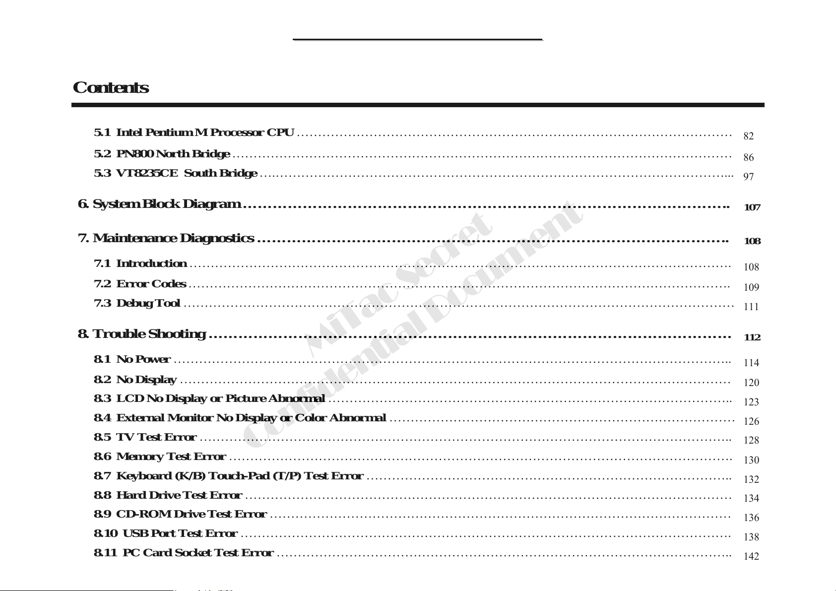
Contents
8666 N/B Maintenance
8666 N/B Maintenance
5.1 Intel Pentium M Processor CPU …………………………………………………………………………………………
5.2 PN800 North Bridge ………………………………………………………………………………………………………
5.3 VT8235CE South Bridge ….……………………………………………………………………………………………...
6. System Block Diagram ……………………………………………………………………………………..
7. Maintenance Diagnostics …………………………………………………………………………………..
7.1 Introduction ……………………………………………………………………………………………………………….
7.2 Error Codes ……………………………………………………………………………………………………………….
7.3 Debug Tool …………………………………………………………………………………………………………………
8. Trouble Shooting ……………………………………………………………………………………………
8.1 No Power …………………………………………………………………………………………………………………..
8.2 No Display …………………………………………………………………………………………………………………
8.3 LCD No Display or Picture Abnormal …………………………………………………………………………………..
8.4 External Monitor No Display or Color Abnormal ………………………………………………………………………
8.5 TV Test Error ……………………………………………………………………………………………………………..
8.6 Memory Test Error ……………………………………………………………………………………………………….
8.7 Keyboard (K/B) Touch-Pad (T/P) Test Error …………………………………………………………………………..
8.8 Hard Drive Test Error ……………………………………………………………………………………………………
8.9 CD-ROM Drive Test Error ………………………………………………………………………………………………
8.10 USB Port Test Error …………………………………………………………………………………………………….
8.11 PC Card Socket Test Error ……………………………………………………………………………………………..
Confidential Document
MiTac Secret
82
86
97
107
108
108
109
111
112
114
120
123
126
128
130
132
134
136
138
142
2
Page 4
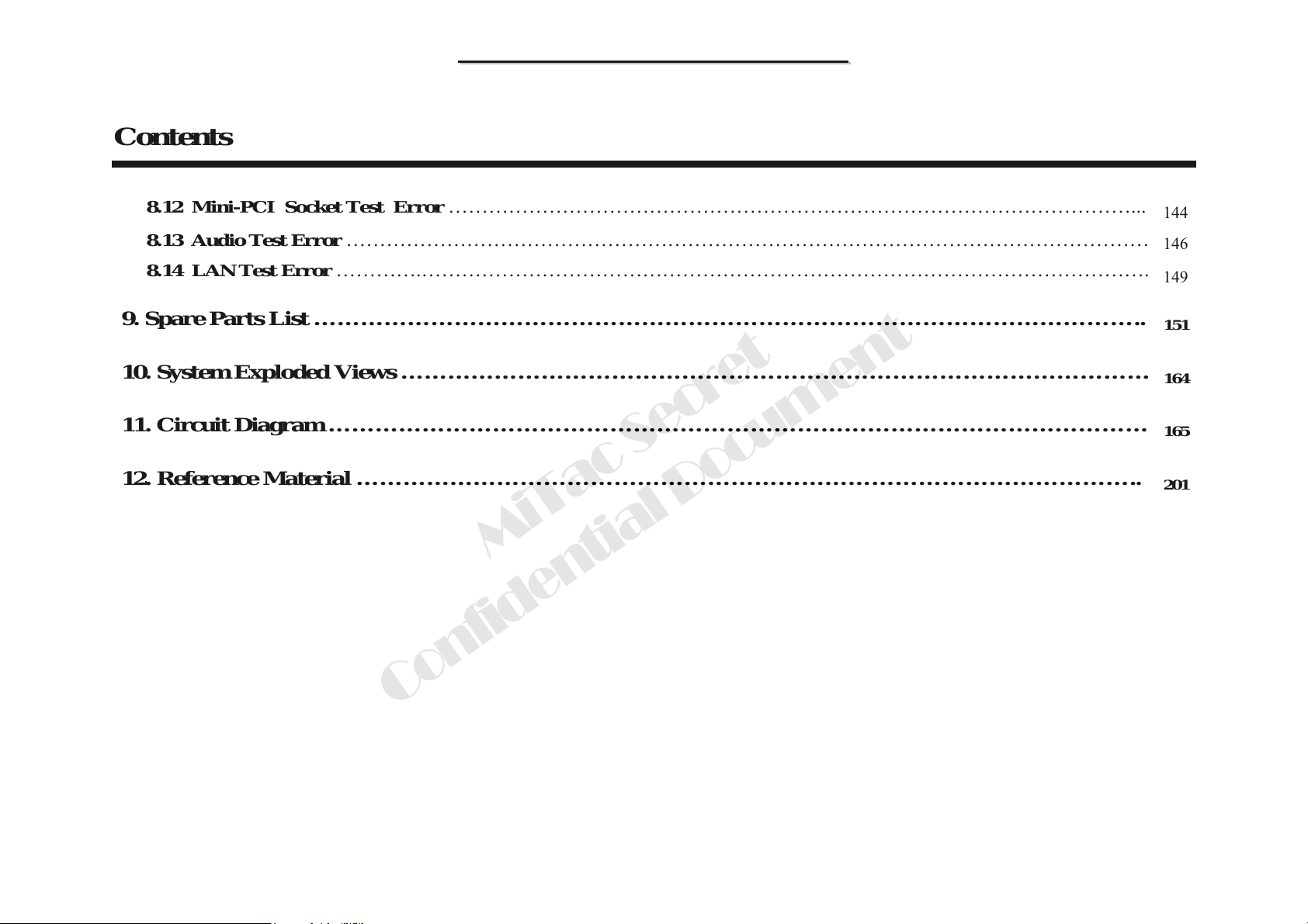
Contents
8666 N/B Maintenance
8666 N/B Maintenance
8.12 Mini-PCI Socket Test Error …………………………………………………………………………………………...
8.13 Audio Test Error …………………………………………………………………………………………………………
8.14 LAN Test Error ………….……………………………………………………………………………………………….
9. Spare Parts List ……………………………………………………………………………… ……………..
10. System Exploded Views ……………………………………………………………………………………
11. Circuit Diagram ……………………………………………………………………………………………
12. Reference Material ………………………………………………………………………………………..
MiTac Secret
144
146
149
151
164
165
201
Confidential Document
3
Page 5

8666 N/B Maintenance
8666 N/B Maintenance
1. Hardware Engineering Specification
1.1 Introduction
1.1.1 General Description
This document describes the brief introduction for MiTAC 8666 portable notebook computer system
1.1.2 System Overview
The MiTAC 8666 model is designed for Intel Mobile Pentium-M Processor Banias 1.3G ~ 1.5GHz or Dothan 1.3G ~
2.1GHz with 400MHz, and Dothan 1.6G ~ 2.1GHz with 533MHz FSB with Micro-FCPGA package.
This system is based on PCI architecture and is fully compatible with IBM PC/AT specification, which has standard
hardware peripheral interface. The power management complies with Advanced Configuration and Power Interface
(ACPI) 2.0. It also provides easy configuration through CMOS setup, which is built in system BIOS software and can
be pop-up by pressing F2 key at system start up or warm reset. System also provides icon LEDs to display system
status, such as Wireless Lan indicator, Power indicator, Battery status indicator, ODD, HDD, Num Lock, Caps Lock,
Scroll Lock, It also equipped with LAN, 56K Fax MODEM, 4 USB ports, S-Video and audio line out, external
microphone function.
The memory subsystem supports two expansion DDR SDRAM slot with unbuffered PC3200 DDR400 SDRAM.
The VIA PN800 Mobile North Bridge integrates a high performance CPU interface for Intel Pentium 4 / Pentium-M
Confidential Document
MiTac Secret
4
Page 6

8666 N/B Maintenance
8666 N/B Maintenance
processor, a full featured AGP port controller, Integrated Graphics with 2D/ 3D/ Video Controllers, a advanced high-
performance DDR400 SDRAM controller, and high bandwidth Ultra V-Link host controller connecting with VIA
VT8235CE South Bridge.
The VIA VT8235CE integrates Universal Serial Bus 2.0 Host Controllers Interface (UHCI), the Audio Controller with
AC97 interface, the Ethernet includes a 32-bit PCI controller, the IDE Master/Slave controllers, and Inter-operable
with VIA Host-to-V-Link Host Controller.
The VIA VT6103L is a Fast Ethernet 10 / 100 1-port PHY / Transceiver with MII interface, and meet all applicable
IEEE 802.3, 10Base-T and 100Base-Tx standards.
The ENE CB1410 CardBus controller functions as a single slot PCI to Cardbus bridge. The CB1410 compliant with
PCI Local Bus Specification Rev2.2, PC99 System Design Guide, and PC Card Standard 8.0.
The W83L950D is a high performance microcontroller on-chip supporting functions optimized for embedded control.
These include ROM, RAM, four types of timers, a serial communication interface, optional I²C bus interface, host
interface, A/D converter, D/A converter, I/O ports, and other functions needed in control system configurations, so
that compact, high performance systems can be implemented easily.
A full set of software drivers and utilities are available to allow advanced operating systems such as Windows ME,
Windows 2000 and Windows XP to take full advantage of the hardware capabilities. Features such as bus mastering
IDE, Plug and Play, Advanced Power Management (APM) with application restart, software-controlled power
shutdown.
Following chapters will have more detail description for each individual sub-systems and functions.
Confidential Document
MiTac Secret
5
Page 7
8666 N/B Maintenance
8666 N/B Maintenance
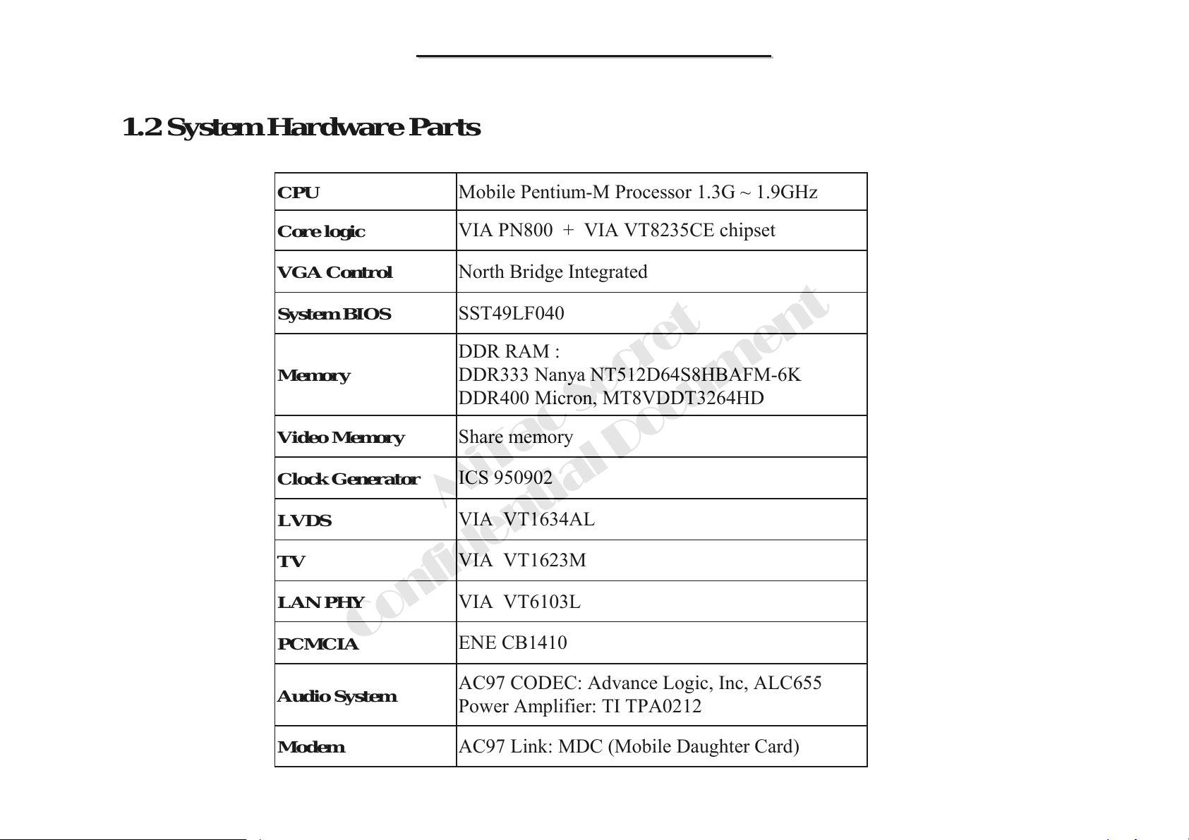
1.2 System Hardware Parts
CPU
Core logic
VGA Control
System BIOS
Memory
Video Memory
Clock Generator
LVDS
TV
Mobile Pentium-M Processor 1.3G ~ 1.9GHz
VIA PN800 + VIA VT8235CE chipset
North Bridge Integrated
SST49LF040
DDR RAM :
DDR333 Nanya NT512D64S8HBAFM-6K
DDR400 Micron, MT8VDDT3264HD
Share memory
ICS 950902
MiTac Secret
VIA VT1634AL
VIA VT1623M
LAN PHY
PCMCIA
Audio System
Modem
Confidential Document
VIA VT6103L
ENE CB1410
AC97 CODEC: Advance Logic, Inc, ALC655
Power Amplifier: TI TPA0212
AC97 Link: MDC (Mobile Daughter Card)!
6
Page 8

8666 N/B Maintenance
8666 N/B Maintenance
1.2.1 Intel Banias Processors in Micro-FCPGA Package
Intel Banias Processors with 593 pins Micro-FCBGA package.
It has the Intel NetBurst micro-architecture which features include hyper-pipelined technology, a rapid execution
engine, a 400MHz system, an execution trace cache, advanced dynamic execution, advanced transfer cache, enhanced
floating point and multi-media unit, and Streaming SIMD Extensions 2 (SSE2).
The Streaming SIMD Extensions 2 (SSE2) enable break-through levels of performance in multimedia applications
including 3-D graphics, video decoding/encoding, and speech recognition.
Use Source-Synchronous Transfer (SST) of address and data to improve performance by transferring data four times
per bus clock.
Support Enhanced Intel SpeedStep technology, which enables real-time dynamic switching of the voltage and
frequency between two performance modes.
MiTac Secret
1.2.2 Clock Generator
The ICS950902 is a single chip clock solution for desktop designs using the VIA P4X/P4M/KT/KN266/333 style
chipsets with PC133 or DDR memory. The ICS950902 is part of a whole new line of ICS clock generators and buffers
called TCH™ (Timing Control Hub). This part incorporates ICS's newest clock technology which offers more robust
features and functionality. Employing the use of a serially programmable I2C interface, this device can adjust the
output clocks by configuring the frequency setting, the output divider ratios, selecting the ideal spread percentage, the
Confidential Document
7
Page 9
8666 N/B Maintenance
8666 N/B Maintenance
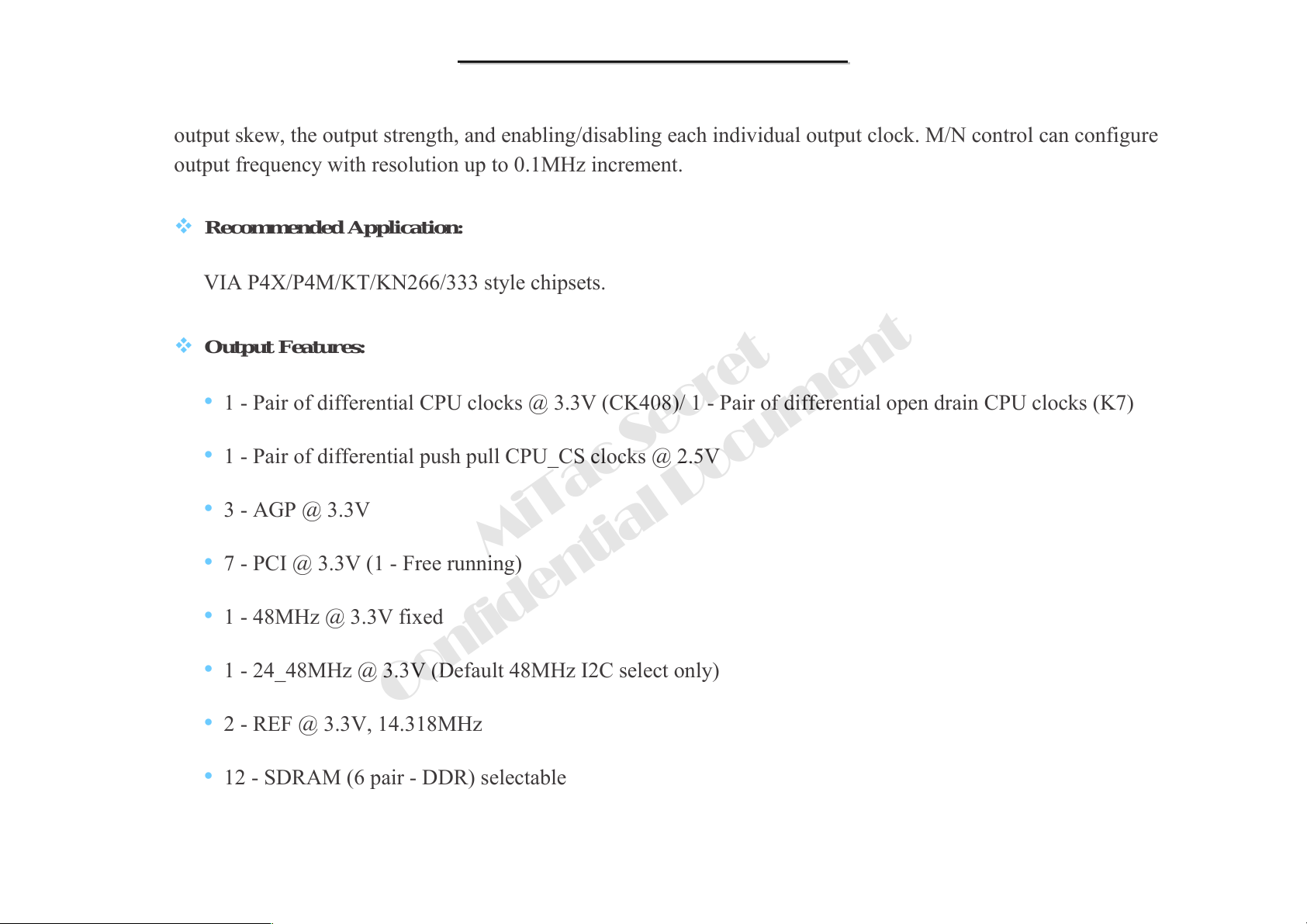
output skew, the output strength, and enabling/disabling each individual output clock. M/N control can configure
output frequency with resolution up to 0.1MHz increment.
Recommended Application:
VIA P4X/P4M/KT/KN266/333 style chipsets.
Output Features:
• 1 - Pair of differential CPU clocks @ 3.3V (CK408)/ 1 - Pair of differential open drain CPU clocks (K7)
• 1 - Pair of differential push pull CPU_CS clocks @ 2.5V
• 3 - AGP @ 3.3V
• 7 - PCI @ 3.3V (1 - Free running)
• 1 - 48MHz @ 3.3V fixed
• 1 - 24_48MHz @ 3.3V (Default 48MHz I2C select only)
MiTac Secret
Confidential Document
• 2 - REF @ 3.3V, 14.318MHz
• 12 - SDRAM (6 pair - DDR) selectable
8
Page 10
8666 N/B Maintenance
8666 N/B Maintenance
Features/Benefits:
• Programmable output frequency.
• Programmable output divider ratios.
• Programmable output rise/fall time.
• Programmable output skew.
• Programmable spread percentage for EMI control.
• DDR output buffer supports up to 200MHz.
• Watchdog timer technology to reset system if system malfunctions.
MiTac Secret
• Programmable watch dog safe frequency.
• Support I2C Index read/write and block read/write operations.
• Uses external 14.318MHz crystal.
Confidential Document
9
Page 11

8666 N/B Maintenance
8666 N/B Maintenance
1.2.3 PN800 Mobile North Bridge
Defines Highly Integrated Solutions for Full Featured Value PC Mobile Designs
• High Performance UMA North Bridge: Integrated Pentium 4 North Bridge with 800 MHz FSB support and
UniChrome Pro 3D / 2D Graphics & Video Controllers in a single chip
• Advanced 64-bit memory controller supporting DDR400 / 333 / 266 SDRAM
• Combines with VIA VT8235-CE / VT8237 South Bridge for integrated 10/100 LAN, Audio, ATA133 IDE,
LPC, USB 2.0 and Serial ATA (VT8237)
• 1.5V Core and Pentium 4 AGTL+ I/O
• 37.5 x 37.5mm HSBGA (Ball Grid Array with Heat Spreader) package with 829 balls and 1mm ball pitch
MiTac Secret
• Pin compatible with PM800, PM880, PN880, PT800A and PT880 Pentium 4 North Bridges
High Performance CPU Interface
• Supports Intel 800 / 533 / 400 MHz FSB Pentium 4 and Pentium M processors
Confidential Document
• Supports Intel Hyper-Threading Technology
• Supports DBI (Dynamic Bus Inversion) and Data, Address, Response Parity
• Twelve outstanding transactions (twelve level In-Order Queue (IOQ) )
10
Page 12
8666 N/B Maintenance
8666 N/B Maintenance
• Built-in Phase Lock Loop circuitry for optimal skew control within and between clocking regions
Full Featured Accelerated Graphics Port (AGP) Controller
• AGP v3.0 compliant 8x / 4x transfer modes with Fast Write support
• 1.5V AGP I/O interface
• Pipelined split-transaction long-burst transfers up to 2.1 GB/sec
• Supports Side Band Addressing (SBA) mode
• Supports Flush / Fence commands
• Supports DBI (Dynamic Bus Inversion)
MiTac Secret
• Asynchronous AGP and CPU interface
• Thirty-two level request queue for read and write
• One-hundred-twenty-eight level (quadwords) of read data FIFO
Confidential Document
• Sixty-four level (quadwords) of write data FIFO
• Graphics Address Relocation Table (GART)
• One level TLB structure
11
Page 13
8666 N/B Maintenance
8666 N/B Maintenance
• Sixteen entry fully associative page table
• LRU replacement scheme
Advanced High-Performance DDR400 SDRAM Controller
• Supports DDR400 / 333 / 266 memory types with 2.5V SSTL-2 DRAM interface
• Supports mixed 64 / 128 / 256 / 512 / 1024Mb DDR SDRAMs in x8 and x16 configurations
• Supports CL 2 / 2.5 for DDR266 / 333 and CL 2.5 / 3 for DDR400
• Supports 4 unbuffered double-sided DIMMs and up to 8 GBytes of physical memory
• Two sets of memory data, address and control signals each of which drives up to 2 DIMMs
MiTac Secret
• Programmable timing / drive for memory address, data and control signals independently for each signal set
• DRAM interface pseudo-synchronous with host CPU for optimal memory performance
• Concurrent CPU, AGP / integrated graphics controller and V-Link access for minimum memory access
latency
• Bank interleave and up to 16-bank page interleave (i.e., 16 pages open simultaneously) based on LRU to
effectively reduce memory access latency
• Seamless DRAM command scheduling for maximum DRAM bus utilization (e.g., precharge other banks
Confidential Document
12
Page 14
8666 N/B Maintenance
8666 N/B Maintenance
while accessing the current bank)
• CPU Read-Around-Write capability for non-stalled operation
• Speculative DRAM read before snoop result to reduce PCI master memory read latency
• Supports Burst Read and Write operations with burst length of 4 or 8
• Twelve cache lines (96 quadwords) of integrated CPU-to-DRAM write buffers and twelve separate cache
lines of CPU-to-DRAM read prefetch buffers
• Optional dynamic Clock Enable (CKE) control for DRAM power reduction during normal system state (S0)
• Supports self-refresh and CAS-before-RAS DRAM refresh with staggered RAS timing
High Bandwidth 1 GB / Sec 16-Bit “Ultra V-Link” Host Controller
• Supports 66 MHz, 4x and 8x transfer modes, Ultra V-Link Host interface with 1 GB/sec total bandwidth
• Full duplex transfers with separate command / strobe for 4x and 8x modes
• Request / Data split transaction
• Transaction assurance for V-Link Host-to-Client access eliminates V-Link Host-Client Retry cycles
• Intelligent V-Link transaction protocol to eliminate data wait-states and throttle transfer latency to avoid data
overflow
Confidential Document
MiTac Secret
13
Page 15

8666 N/B Maintenance
8666 N/B Maintenance
• Highly efficient V-Link arbitration with minimum overhead
Advanced System Power Management Support
• ACPI 2.0 and PCI Bus Power Management 1.1 compliant
• Supports Suspend-to-DRAM (STR) and DRAM self-refresh
• Supports dynamic Clock Enable (CKE) control for DRAM power reduction during normal system state (S0)
• Supports SMI, SMM, and STPCLK mechanisms
• Supports Enhanced Intel Speedstep™ Technology
• Low-leakage I/O pads
MiTac Secret
Integrated Graphics with 2D / 3D / Video Controllers
• Optimized Unified Memory Architecture (UMA)
• Supports 16 / 32 / 64 MB Frame Buffer sizes
• 200 MHz Graphics Engine Clock
• Two independent 128-bit data paths between North Bridge and graphics core to improve video performance,
one for frame buffer access and one for texture / command access
Confidential Document
14
Page 16
8666 N/B Maintenance
8666 N/B Maintenance
• PCI v2.2 compliant (for control and configuration)
• AGP v3.0 compliant (for control and data transfer)
2D Acceleration
• 128-bit 2D graphics engine
• Hardware 2D rotation
• Supports ROP3, 256 operations
• Supports 8bpp, 15/16bpp and 32bpp color depth modes
• BitBLT (Bit BLock Transfer) functions including alpha BLTs
MiTac Secret
• True-color hardware cursor (64x64x32bpp) with 256-level blending effect
• Color expansion, source Color Key and destination Color Key
• Bresenham line drawing / style line function
Confidential Document
• Transparency mode
• Window clipping
• Text function
15
Page 17
3D Acceleration
• 3D Graphics Proces sor
– 128-bit 3D graphics engine
– Dual pixel rendering pipes
– Dual texture units
– Floating-point setup engine
– Internal full 32-bit ARGB format for high rendering quality
– 8K Texture Cache
• Capability
8666 N/B Maintenance
8666 N/B Maintenance
– Supports ROP2
– Supports various texture formats including 16/32bpp ARGB, 8bpp Palletized (ARGB), YUV 422/420 and
compressed texture (DXTC)
– Texture sizes up to 2048x2048
– Microsoft DirectX texture compression
– High quality texture filter for Nearest, Linear, Bi-linear, Tri-linear, and Anisotropic modes
– Flat and Gouraud shading
– Vertex Fog and Fog Table
– Z-Bias, LOD-Bias, Polygon offset, Edge Anti-aliasing and Alpha Blending
– Bump mapping and cubic mapping
Confidential Document
MiTac Secret
16
Page 18

– Hardware back-face culling
– Specular lighting
• Performance
– Two textures per pass
– Triangle rate up to 4.5 million triangles per second
– Pixel rate up to 200 million pixels per second for 2 textures each
– Texel bilinear fill rate up to 400 million texels per second
– High quality dithering
Video Acceleration
8666 N/B Maintenance
8666 N/B Maintenance
• High Quality Video Process or
MiTac Secret
– RGB555, RGB565, RGB8888 and YUV422 video playback formats
– High quality 5-tap horizontal and 5-tap vertical scaler (up or down) for both horizontal and vertical scaling
(linear interpolation for horizontal and vertical p-scaling and filtering for horizontal and vertical down-
scaling)
– Independent graphics and video gamma tables
– 2 sets of Color and Chroma Key support
– Color enhancement for contrast, hue, saturation and brightness
– YUV-to-RGB color space conversion
– Display rotation in clockwise and counter-clockwise directions
Confidential Document
17
Page 19
8666 N/B Maintenance
8666 N/B Maintenance
– Bob, Weave, Median-filter and Adaptive de-interlacing modes
– 3:2 / 2:2 pull-down detection
– De-blocking mode support
– Combining of many special effects such as filter, scaling up or down, sub-picture blending, de-interlacing
and deblocking to one pass process
– Tear-free double / triple buffer flipping
– Input video vertical blanking or line interrupt
– Video gamma correction
• Video Overlay
– Simultaneous graphics and TV video playback overlay
– Supports video window overlays
– Supports both YUV and RGB format Chroma Key
– Supports 16 operations for Color and Chroma Key
– Hardware sub-picture blending
MiTac Secret
• MPEG Video Playback
– MPEG-2 hardware VLD (Various Length Decode), iDCT, and motion compensation for full speed DVD
and MPEG-2 playback at full D1 resolution
– MPEG-4 ASP (Advanced Simple Profile) Level 5 with GMC (Global Motion Compensation) L0/L1 and ¼
pixel MC support for high video quality and performance
– High quality DVD and streaming video playback
Confidential Document
18
Page 20
8666 N/B Maintenance
8666 N/B Maintenance
– DVD playback auto-flipping
– DVD sub-picture playback overlay
• Video Capture Capability
– 8-bit capture port following ITU-R BT656, VIP 1.1 and VIP 2.0 standards supporting 16 / 32-bit RGB and
YUV422 video capture formats
– Video capture and playback tear free auto flipping
– Multiplexed on Digital Video Port 0 (DVP0 selectable as Capture-In or TV-Out)
– External Hsync / Vsync support
Advanced Graphics Power Management Support
• Built-in reference voltage generator and monitor sense circuits
• Automatic panel power sequencing and VESA DPMS (Display Power Management Signaling) CRT power-
down
• External I/O signal controls enabling of graphics accelerator into standby / suspend-off state
• Dynamic clock gating for inactive functions to achieve maximum power savings
• I2C Serial Bus and DDC / E-DDC Monitor Communications for Plug-and-Play configuration
Confidential Document
MiTac Secret
19
Page 21
8666 N/B Maintenance
8666 N/B Maintenance
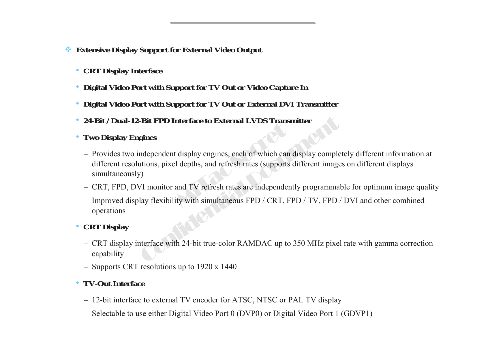
Extensive Display Support for External Video Output
• CRT Display Interface
• Digital Video Port with Support for TV Out or Video Capture In
• Digital Video Port with Support for TV Out or External DVI Transmitter
• 24-Bit / Dual-12-Bit FPD Interface to External LVDS Transmitter
• Two Display En gines
– Provides two independent display engines, each of which can display completely different information at
different resolutions, pixel depths, and refresh rates (supports different images on different displays
simultaneously)
– CRT, FPD, DVI monitor and TV refresh rates are independently programmable for optimum image quality
– Improved display flexibility with simultaneous FPD / CRT, FPD / TV, FPD / DVI and other combined
MiTac Secret
operations
• CRT Display
– CRT display interface with 24-bit true-color RAMDAC up to 350 MHz pixel rate with gamma correction
capability
Confidential Document
– Supports CRT resolutions up to 1920 x 1440
• TV-Out Interface
– 12-bit interface to external TV encoder for ATSC, NTSC or PAL TV display
– Selectable to use either Digital Video Port 0 (DVP0) or Digital Video Port 1 (GDVP1)
20
Page 22
8666 N/B Maintenance
8666 N/B Maintenance
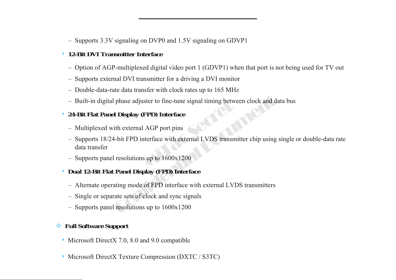
– Supports 3.3V signaling on DVP0 and 1.5V signaling on GDVP1
• 12-Bit DVI Transmitter Interface
– Option of AGP-multiplexed digital video port 1 (GDVP1) when that port is not being used for TV out
– Supports external DVI transmitter for a driving a DVI monitor
– Double-data-rate data transfer with clock rates up to 165 MHz
– Built-in digital phase adjuster to fine-tune signal timing between clock and data bus
• 24-Bit Flat Panel Display (FPD) Interface
– Multiplexed with external AGP port pins
– Supports 18/24-bit FPD interface with external LVDS transmitter chip using single or double-data rate
data transfer
– Supports panel resolutions up to 1600x1200
MiTac Secret
• Dual 12-Bit Flat Panel Display (FPD) Interface
– Alternate operating mode of FPD interface with external LVDS transmitters
– Single or separate sets of clock and sync signals
– Supports panel resolutions up to 1600x1200
Confidential Document
Full Software Support
• Microsoft DirectX 7.0, 8.0 and 9.0 compatible
• Microsoft DirectX Texture Compression (DXTC / S3TC)
21
Page 23
8666 N/B Maintenance
8666 N/B Maintenance
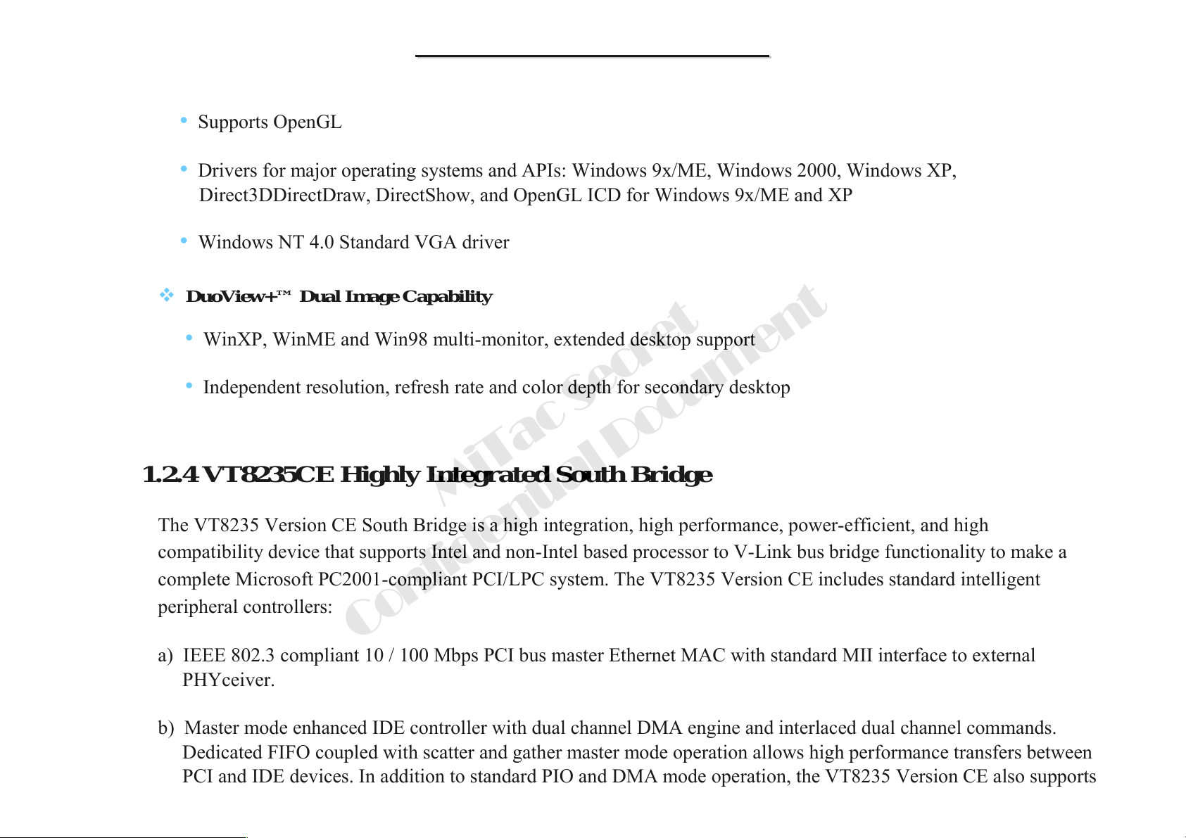
• Supports OpenGL
• Drivers for major operating systems and APIs: Windows 9x/ME, Windows 2000, Windows XP,
Direct3DDirectDraw, DirectShow, and OpenGL ICD for Windows 9x/ME and XP
• Windows NT 4.0 Standard VGA driver
DuoView+™ Dual Image Capability
• WinXP, WinME and Win98 multi-monitor, extended desktop support
• Independent resolution, refresh rate and color depth for secondary desktop
1.2.4 VT8235CE Highly Integrated South Bridge
MiTac Secret
The VT8235 Version CE South Bridge is a high integration, high performance, power-efficient, and high
compatibility device that supports Intel and non-Intel based processor to V-Link bus bridge functionality to make a
complete Microsoft PC2001-compliant PCI/LPC system. The VT8235 Version CE includes standard intelligent
peripheral controllers:
Confidential Document
a) IEEE 802.3 compliant 10 / 100 Mbps PCI bus master Ethernet MAC with standard MII interface to external
PHYceiver.
b) Master mode enhanced IDE controller with dual channel DMA engine and interlaced dual channel commands.
Dedicated FIFO coupled with scatter and gather master mode operation allows high performance transfers between
PCI and IDE devices. In addition to standard PIO and DMA mode operation, the VT8235 Version CE also supports
22
Page 24
8666 N/B Maintenance
8666 N/B Maintenance
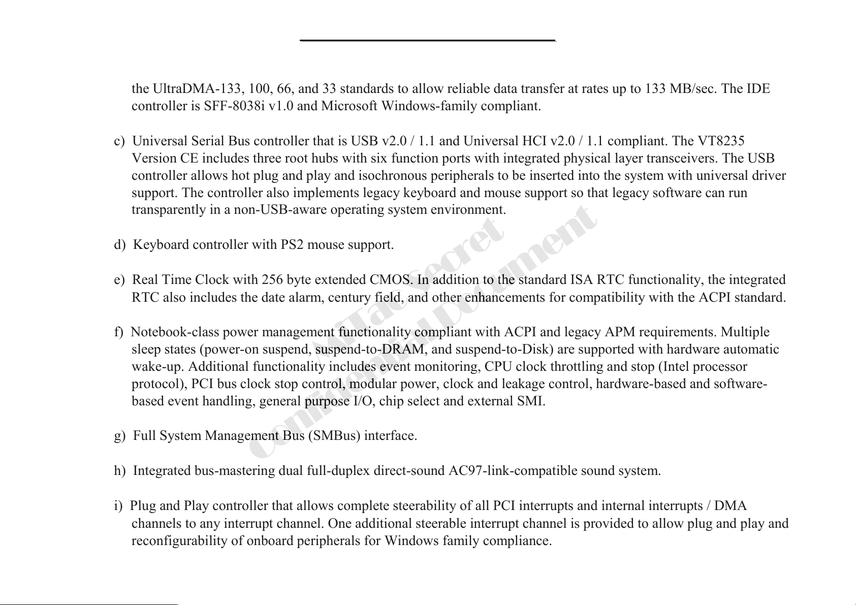
the UltraDMA-133, 100, 66, and 33 standards to allow reliable data transfer at rates up to 133 MB/sec. The IDE
controller is SFF-8038i v1.0 and Microsoft Windows-family compliant.
c) Universal Serial Bus controller that is USB v2.0 / 1.1 and Universal HCI v2.0 / 1.1 compliant. The VT8235
Version CE includes three root hubs with six function ports with integrated physical layer transceivers. The USB
controller allows hot plug and play and isochronous peripherals to be inserted into the system with universal driver
support. The controller also implements legacy keyboard and mouse support so that legacy software can run
transparently in a non-USB-aware operating system environment.
d) Keyboard controller with PS2 mouse support.
e) Real Time Clock with 256 byte extended CMOS. In addition to the standard ISA RTC functionality, the integrated
RTC also includes the date alarm, century field, and other enhancements for compatibility with the ACPI standard.
f) Notebook-class power management functionality compliant with ACPI and legacy APM requirements. Multiple
sleep states (power-on suspend, suspend-to-DRAM, and suspend-to-Disk) are supported with hardware automatic
wake-up. Additional functionality includes event monitoring, CPU clock throttling and stop (Intel processor
protocol), PCI bus clock stop control, modular power, clock and leakage control, hardware-based and software-
based event handling, general purpose I/O, chip select and external SMI.
g) Full System Management Bus (SMBus) interface.
MiTac Secret
Confidential Document
h) Integrated bus-mastering dual full-duplex direct-sound AC97-link-compatible sound system.
i) Plug and Play controller that allows complete steerability of all PCI interrupts and internal interrupts / DMA
channels to any interrupt channel. One additional steerable interrupt channel is provided to allow plug and play and
reconfigurability of onboard peripherals for Windows family compliance.
23
Page 25
8666 N/B Maintenance
8666 N/B Maintenance
The VT8235 Version CE also enhances the functionality of the standard ISA peripherals. The integrated interrupt
controller supports both edge and level triggered interrupts channel by channel. The integrated DMA controller
supports type F DMA in addition to standard ISA DMA modes. Compliant with the PCI-2.2 specification, the VT8235
Version CE supports delayed transactions and remote power management so that slower ISA peripherals do not block
the traffic of the PCI bus. Special circuitry is built in to allow concurrent operation without causing dead lock even in
a PCI-to-PCI bridge environment. The chip also includes eight levels (doublewords) of line buffers from the PCI bus
to the ISA bus to further enhance overall system performance.
1.2.5 CardBus: CB1410
Features:
3.3V operation with 5V tolerant
LFBGA 144-ball package
• Compliant with
– PCI Local Bus Specification, Revision 2.2
– PCI Bus Power Management Interface Specification, Revision 1.1
Confidential Document
– PCI Mobile Design Guide, Version 1.1
– Advanced Configuration and Power Interface Specification, Revision 1.0
– PC 99 System Design Guide
– PC Card Standard 8.0
MiTac Secret
24
Page 26
8666 N/B Maintenance
8666 N/B Maintenance
• Interrupt Configuration
– Supports parallel PCI interrupts
– Supports parallel IRQ and parallel PCI interrupts
– Supports serialized IRQ and parallel PCI interrupts
– Supports serialized IRQ and PCI interrupts
• Power Management Control Logic
– Supports CLKRUN# protocol
– Supports SUSPEND#
– Supports PCI PME# from D3, D2, D1 and D0
– Supports PCI PME# from D3Cold
– Supports D3STATE# (CB1410 only)
MiTac Secret
• Power Switch Interface
– CB1410 supports parallel 4 wire power switch interface.
• Misc Control Logic
– Supports serial EEPROM interface
– Supports socket activity LED
– Supports 5 GPIOs and GPE#
– Supports SPKROUT, CAUDIO and RIOUT#
– Supports PCI LOCK#
Confidential Document
25
Page 27

8666 N/B Maintenance
8666 N/B Maintenance
1.2.6 AC’97 Audio System: Advance Logic, Inc, ALC65
The ALC655 is a 16-bit, full duplex AC'97 2.3 compatible six channels audio CODEC designed for PC multimedia
systems,including host/soft audio and AMR/CNR based designs. The ALC655 incorporates proprietary converter
technology to meet performance requirements on PC99/2001 systems. The ALC655 CODEC provides three pairs of
stereo outputs with 5-Bitvolume controls, a mono output, and multiple stereo and mono inputs, along with flexible
mixing, gain and mute functions to provide a complete integrated audio solution for PCs. The digital interface
circuitry of the ALC655 CODEC operates from a 3.3V power supply for use in notebook and PC applications. The
ALC655 integrates 50mW/20ohm headset audio amplifiers at Front-Out and Surr-Out, built-in 14.318M 24.576MHz
PLL and PCBEEP generator, those can save BOM costs. The ALC655 also supports the S/PDIF input and output
function, which can offer easy connection of PCs to consumer electronic products, such as AC3 decoder/speaker and
mini disk devices. ALC655 supports host/soft audio from Intel ICHx chipsets as well as audio controller based
VIA/SIS/ALI/AMD/nVIDIA/ATI chipset. Bundled Windows series drivers (WinXP/ME/2000/98/NT), EAX/
Direct Sound 3D/ I3DL2/ A3D compatible sound effect utilities (supporting Karaoke, 26-kind of environment sound
emulation,10-band equalizer), HRTF 3D positional audio and Sensaura™ 3D (optional) provide an excellent
entertainment package and game experience for PC users. Besides, ALC655 includes Realtek’s impedance sensing
techniques that makes device load on outputs and inputs can be detected.
• Meets performance requirements for audio on PC99/2001 systems
• Meets Microsoft WHQL/WLP 2.0 audio requirements
• 16-bit Stereo full-duplex CODEC with 48KHz sampling rate
• Compliant with AC’97 2.3 specifications
Confidential Document
MiTac Secret
26
Page 28
8666 N/B Maintenance
8666 N/B Maintenance
– 14.318MHz- 24.576MHz PLL to save crystal
– 12.288MHz BITCLK input can be consumed
– Integrated PCBEEP generator to save buzzer
– Interrupt capability
• Three analog line-level stereo inputs with 5-bit volume control: LINE_IN, CD, AUX
• High quality differential CD input
• Two analog line-level mono input: PCBEEP,PHONE-IN
• Two software selectable MIC inputs applications (software selectable)
• Boost preamplifier for MIC input 50mW/20 amplifier
MiTac Secret
• External Amplifier Power Down (EAPD) capability
• Power management and enhanced power saving features
• Stereo MIC record for AEC/BF application
Confidential Document
• Supports Power Off CD function
• Adjustable VREFOUT control Supports double sampling rate (96KHz) of DVD audio playback
• Support 48KHz of S/PDIF output is compliant with AC’97 rev2.3 specification
27
Page 29
8666 N/B Maintenance
8666 N/B Maintenance
• Power support: Digital: 3.3V; Analog: 3.3V/5V
1.2.7 MDC: PCTEL Modem Daughter Card PCT2303W (ASKEY V1456VQL-P1)
The PCT2303W chipset is designed to meet the demand of this emerging worldwide AMR/MDC market. The
combination of PC-TEL’s well proven PCT2303W chipset and the HSP56TM MR software modem driver allows
systems manufactures to implement modem functions in PCs at a lower bill of materials (BOM) while maintaining
higher system performance.
PC-TEL has streamlined the traditional modem into the Host Signal Processing (HSP) solution. Operating with the
Pentium class processors, HSP becomes part of the host computer’s system software. It requires less power to operate
and less physical space than standard modem solutions. PC-TEL’s HSP modem is an easily integrated, cost-effective
communications solution that is flexible enough to carry you into the future.
MiTac Secret
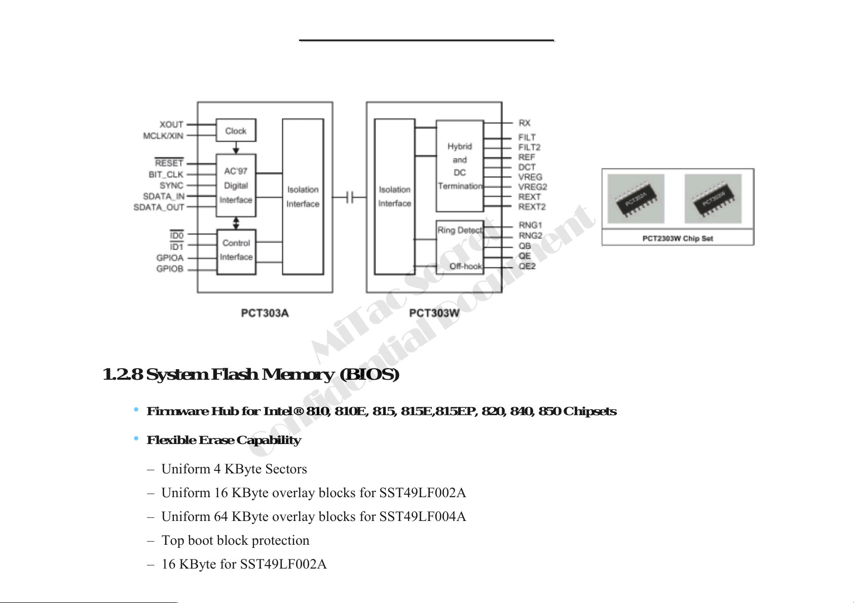
The PCT2303W chip set is an integrated direct access arrangement (DAA) and Codec that provides a programmable
line interface to meet international telephone line requirements. The PCT2303W chip set is available in two 16-pin
small outline packages (AC’97 interface on PCT303A and phone-line interface on PCT303W). The chip set eliminates
the need for an AFE, an isolation transformer, relays, opto-isolators, and 2-to 4-wire hybrid. The PCT2303W chip set
dramatically reduces the number of discrete components and cost required to achieve compliance with international
regulatory requirements. The PCT2303W complies with AC’97 Interface specification Rev. 2.1.
The chip set is fully programmable to meet world-wide telephone line interface requirements including those
described by CTR21, NET4, JATE, FCC, and various country-specific PTT specifications. The programmable
parameters of the PCT2303W chip set include AC termination, DC termination, ringer impedance, and ringer
Confidential Document
28
Page 30
8666 N/B Maintenance
8666 N/B Maintenance
threshold. The PCT2303W chip set has been designed to meet stringent world-wide requirements for out-of-band
energy, billing-tone immunity, lightning surges, and safety requirements.
Features:
Virtual com port with a DTE throughout up to 460.8Kbps.
G3 Fax compatible
Auto dial and auto answer
Ring detection
Codec/DAA Features
• AC97 2.1 compliant
• 86dB dynamic range TX/RX paths
• 2-4-wire hybrid
• Integrated ring detector
MiTac Secret
Confidential Document
• High voltage isolation of 4000V
• Support for “Caller ID”
• Compliant with FCC Part68, CTR21, Net4 and JATE
29
Page 31
8666 N/B Maintenance
8666 N/B Maintenance
• Low power standby
• Low profile SOIC package 16 pins 10x3x1.55mm
• Low power consumption
• 10mA @ 3.3V operation
• 1mA @ 3.3V power down
• Integrated modem codec
Standard Features
• Data
– ITU-T V.90 (56Kbps), V.34 (4.8Kbps TO 33.6 Kbps), V.32 bis (4.8Kbps to 14.4Kbps), V.22 bis (1.2 bps
to 2.4 Kbps), V.21 and Bell 103 and 212A(300 to 1200 bps) modulation protocol
– Data Compression ITU-T V.42bis MNP Class 5
– Error Correction ITU-T V.42 LAPM MNP 2-4
• Fax
– ITU-T V. 17, V.29, V.27ter, V.21, Channel 2, Group 3, EIA Class I
Confidential Document
MiTac Secret
30
Page 32
8666 N/B Maintenance
8666 N/B Maintenance
MiTac Secret
1.2.8 System Flash Memory (BIOS)
• Firmware Hub for Intel® 810, 810E, 815, 815E,81 5EP, 820, 840, 850 Chipsets
• Flexible Erase Capability
Confidential Document
– Uniform 4 KByte Sectors
– Uniform 16 KByte overlay blocks for SST49LF002A
– Uniform 64 KByte overlay blocks for SST49LF004A
– Top boot block protection
– 16 KByte for SST49LF002A
31
Page 33
8666 N/B Maintenance
8666 N/B Maintenance
– 64 KByte for SST49LF004A
– Chip-Erase for PP Mode
• Single 3.0-3.6V Read and Write Operations
• Superior Reliability
• Firmware Hub Hardware Interface Mode
– 5-signal communication interface supporting byte Read and Write
– 33 MHz clock frequency operation
– WP# and TBL# pins provide hardware write protect for entire chip and/or top Boot Block
– Block Locking Register for all blocks
– Standard SDP Command Set
– Data# Polling and Toggle Bit for End-of-Write detection
MiTac Secret
– 5 GPI pins for system design flexibility
– 4 ID pins for multi-chip selection
Confidential Document
32
Page 34
8666 N/B Maintenance
8666 N/B Maintenance
1.2.9 Memory System
1.2.9.1 64MB, 128MB, 256MB, 512MB (x64) 200-Pin DDR SDRAM SODIMMs
•
JEDEC-standard 200-pin, small-outline, dual in-line memory module (SODIMM)
• Utilizes 200 Mb/s and 266 Mb/s DDR SDRAM components
• 64MB (8 Meg x 64 [H]); 128MB (16 Meg x 64, [H] and [HD]); 256MB (32 Meg x 64 [HD]); 512MB (64
Meg x 64 [HD])
• VDD= VDDQ= +2.5V ±0.2V
• VDDSPD = +2.2V to +5.5V
• 2.5V I/O (SSTL_2 compatible)
• Commands entered on each positive CK edge
• DQS edge-aligned with data for READs; center-aligned with data for WRITEs
• Internal, pipelined double data rate (DDR) architecture; two data accesses per clock cycle
• Bidirectional data strobe (DQS) transmitted/received with data—i.e.,source-synchronous data capture
• Differential clock inputs (CK and CK# - can be multiple clocks, CK0/CK0#, CK1/CK1#, etc.)
• Four internal device banks for concurrent operation
Confidential Document
MiTac Secret
33
Page 35
8666 N/B Maintenance
8666 N/B Maintenance
• Selectable burst lengths: 2, 4, or 8
• Auto precharge option
• Auto Refresh and Self Refresh Modes
• 15.6µs (MT4VDDT864H, MT8VDDT1664HD), 7.8125µs (MT4VDDT1664H, MT8VDDT3264HD,
MT8VDDT6464HD) maximum average periodic refresh interval
• Serial Presence Detect (SPD) with EEPROM
• Fast data transfer rates PC2100 or PC1600
• Selectable READ CAS latency for maximum compatibility
• Gold-plated edge contacts
MiTac Secret
1.2.10 PHY: 3.3-V 10Base-T/100Base-TX Integrated PHY Receiver is a
Low-power, Physical-layer Device (PHY)
Confidential Document
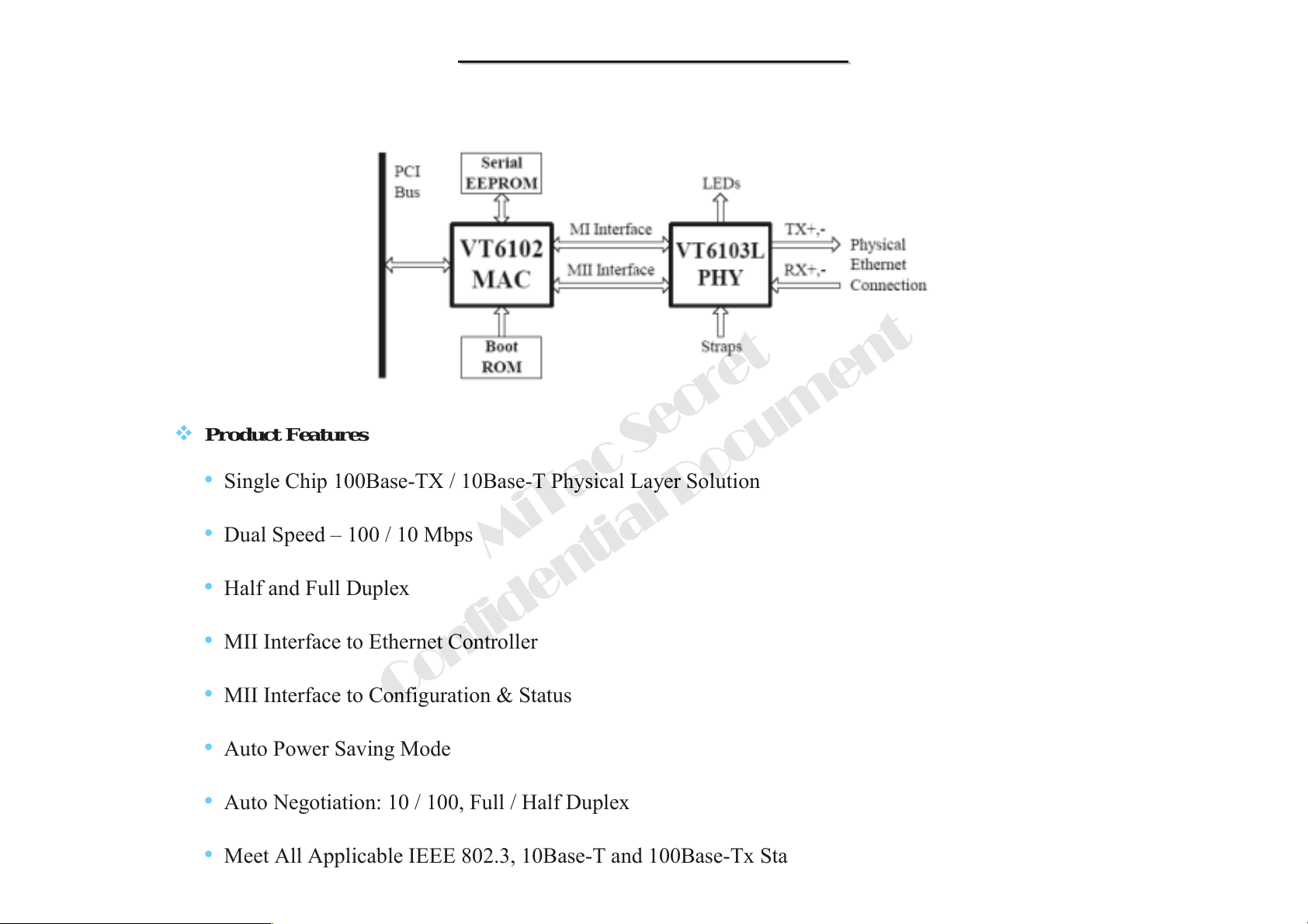
The VT6103L is a Physical Layer device for Ethernet 10Base-T and 100Base-TX using category 5 Unshielded and
Type 1 Shielded cables. This VLSI device is designed for easy implementation of 10 / 100 Mb/s Fast Ethernet LANs.
It interfaces to a MAC through an MII interface ensuring interoperability between products from different vendors.
34
Page 36
8666 N/B Maintenance
8666 N/B Maintenance
Product Features
• Single Chip 100Base-TX / 10Base-T Physical Layer Solution
• Dual Speed – 100 / 10 Mbps
MiTac Secret
• Half and Full Duplex
• MII Interface to Ethernet Controller
• MII Interface to Configuration & Status
• Auto Power Saving Mode
• Auto Negotiation: 10 / 100, Full / Half Duplex
• Meet All Applicable IEEE 802.3, 10Base-T and 100Base-Tx Sta
Confidential Document
35
Page 37
8666 N/B Maintenance
8666 N/B Maintenance
• On Chip Wave Shaping – No External Filters Required
• Adaptive Equalizer
• Baseline Wander Correction
• LED Outputs
– Link Status
– Duplex status
– Speed Status
– Collision
• 48 Pin LQFP Package
MiTac Secret
1.2.11 Keyboard System: Winbond W83L950D
The Winbond Keyboard controller architecture consists of a Turbo 51 core controller surrounded by various registers,
nine general purpose I/O port, 2k+256 bytes of RAM, four timer/counters, dual serial ports, 40K MTP-ROM that is
Confidential Document
divided into four banks, two SMBus interface for master and slave, Support 4 PWM channels, 2 D-A and 8 A-D
converters
36
Page 38
8666 N/B Maintenance
8666 N/B Maintenance
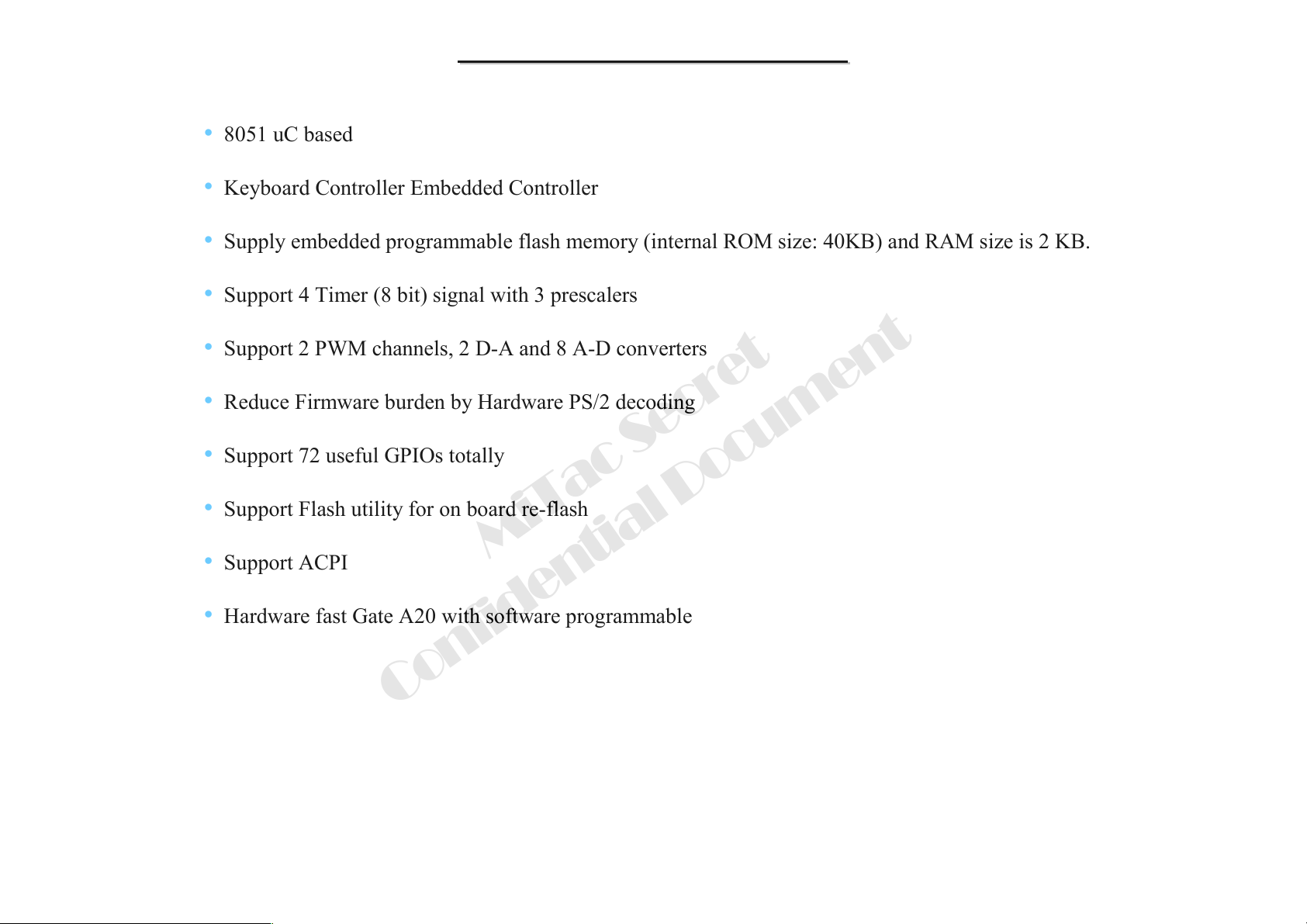
• 8051 uC based
• Keyboard Controller Embedded Controller
• Supply embedded programmable flash memory (internal ROM size: 40KB) and RAM size is 2 KB.
• Support 4 Timer (8 bit) signal with 3 prescalers
• Support 2 PWM channels, 2 D-A and 8 A-D converters
• Reduce Firmware burden by Hardware PS/2 decoding
• Support 72 useful GPIOs totally
• Support Flash utility for on board re-flash
• Support ACPI
• Hardware fast Gate A20 with software programmable
MiTac Secret
Confidential Document
37
Page 39
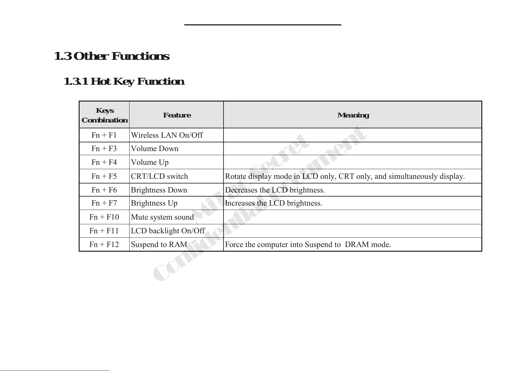
1.3 Other Functions
1.3.1 Hot Key Function
8666 N/B Maintenance
8666 N/B Maintenance
Keys
Combination
Fn + F1 Wireless LAN On/Off
Fn + F3 Volume Down
Fn + F4 Volume Up
Fn + F5 CRT/LCD switch Rotate display mode in LCD only, CRT only, and simultaneously display.
Fn + F6 Brightness Down Decreases the LCD brightness.
Fn + F7 Brightness Up Increases the LCD brightness.
Fn + F10 Mute system sound
Fn + F11 LCD backlight On/Off
Fn + F12 Suspend to RAM Force the computer into Suspend to DRAM mode.
Feature Meaning
MiTac Secret
Confidential Document
38
Page 40
8666 N/B Maintenance
8666 N/B Maintenance
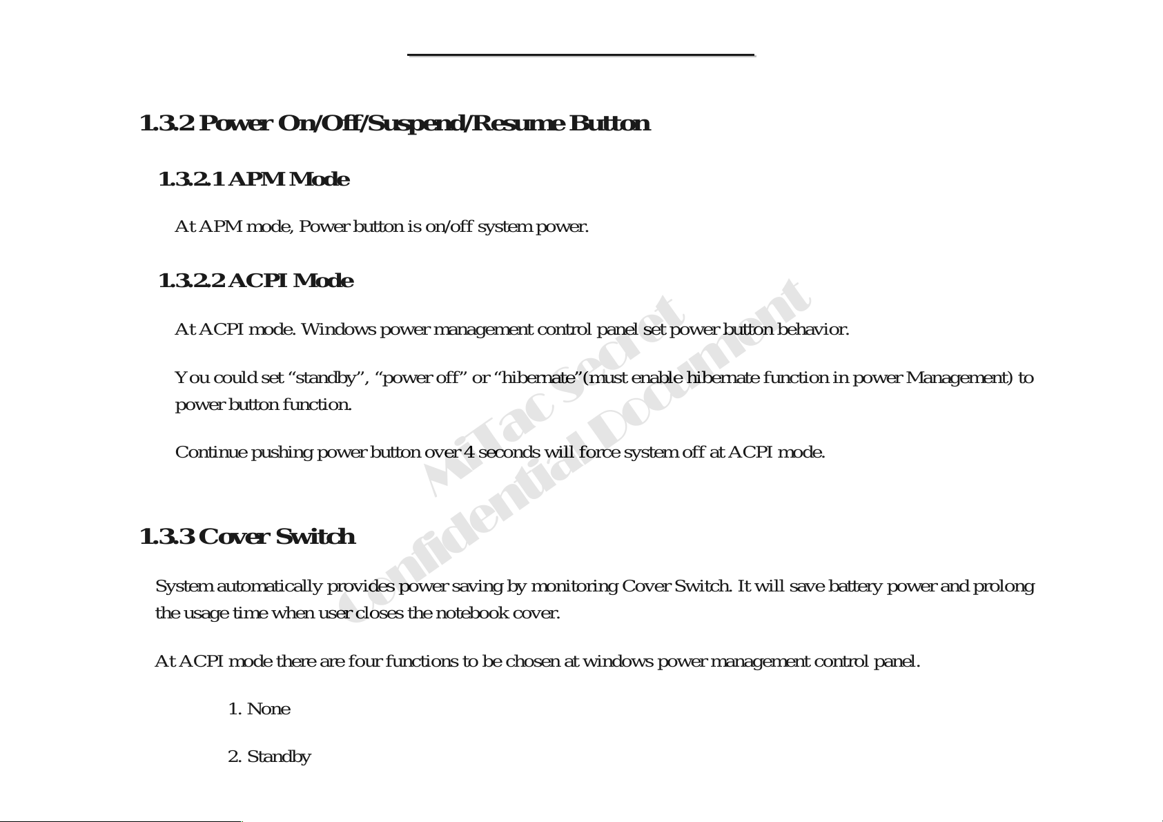
1.3.2 Power On/Off/Suspend/Resume Button
1.3.2.1 APM Mode
At APM mode, Power button is on/off system power.
1.3.2.2 ACPI Mode
At ACPI mode. W indows power managem ent control panel set power button behavior.
You could set “standby”, “power off” or “hibernate”(must enable hibernate function in power Management) to
power button function.
Continue pushi ng power button over 4 seconds will force system off at ACPI mode.
MiTac Secret
1.3.3 Cover Switch
System automatically provides power saving by monitoring Cover Switch. It will save battery power and prolong
the usage time when user closes the notebook cover.
At ACPI mode there are four functions to be chosen at w indows power management control panel.
1. None
2. Standby
Confidential Document
39
Page 41
8666 N/B Maintenance
8666 N/B Maintenance
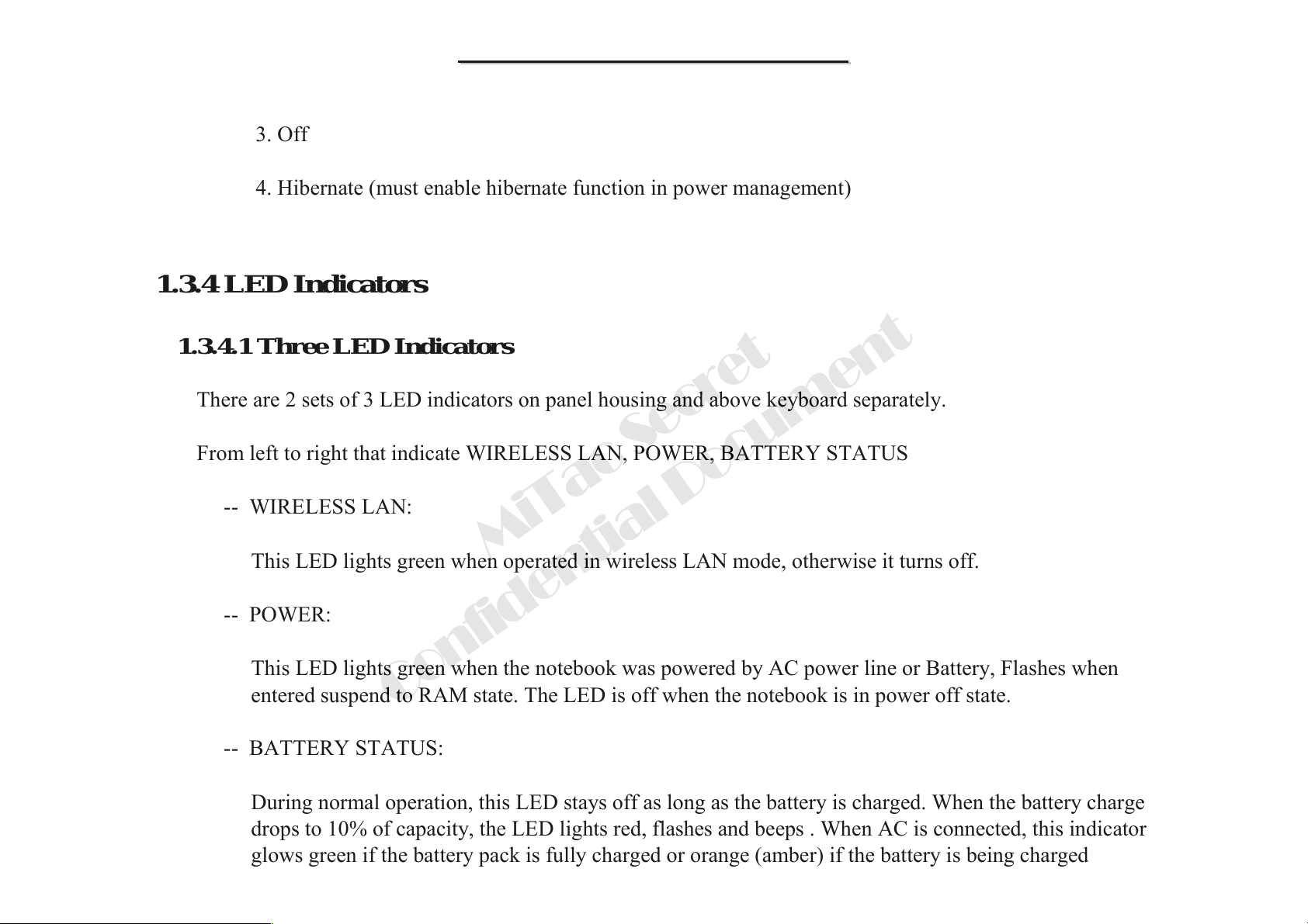
3. Off
4. Hibernate (must enable hibernate function in power management)
1.3.4 LED Indicators
1.3.4.1 Three LED Indicators
There are 2 sets of 3 LED indicators on panel housing and above keyboard separately.
From left to right that indicate WIRELESS LAN, POWER, BATTERY STATUS
-- WIRELESS LAN:
This LED lights green when operated in wireless LAN mode, otherwise it turns off.
-- POWER:
This LED lights green when the notebook was powered by AC power line or Battery, Flashes when
entered suspend to RAM state. The LED is off when the notebook is in power off state.
-- BATTERY STATUS:
During normal operation, this LED stays off as long as the battery is charged. When the battery charge
drops to 10% of capacity, the LED lights red, flashes and beeps . When AC is connected, this indicator
glows green if the battery pack is fully charged or orange (amber) if the battery is being charged
Confidential Document
MiTac Secret
40
Page 42

8666 N/B Maintenance
8666 N/B Maintenance
1.3.4.2 Five LED Indicators:
System has 5 status LED indicators at front side which to display system activity. From left to right that indicate
CD-ROM, HARD DISK, NUM LOCK, CAPS LOCK, SCROLL LOCK.
1.3.5 Battery Status
1.3.5.1 Battery Warning
-- System also provides Battery capacity monitoring and gives users a warning signal to alarm they to
store data before battery dead. This function also protects system from mal-function while battery
capacity is low.
-- Battery Warning: Capacity below 10%, Battery Capacity LED flashes , and system beeps.
MiTac Secret
-- System will Suspend to HDD after 2 Minutes to protect users data.
1.3.5.2 Battery Low State
After Battery Warning State, and battery capacity is below 5%, system will generate beep sound.
1.3.5.3 Battery Dead State
When the battery voltage level reaches 11.5 volts, system will shut down automatically in order to extend the
battery packs' life.
Confidential Document
41
Page 43
8666 N/B Maintenance
8666 N/B Maintenance
1.3.6 Fan Power On/Off Management
FAN is controlled by W83L950D embedded controller-using ADT7460 to sense CPU temperature and PWM control
fan speed. Fan speed is depended on CPU temperature. Higher CPU temperature faster Fan Speed.
1.3.7 CMOS Battery
CR2032 3V 220mAh lithium battery
When AC in or system main battery inside, CMOS battery will consume no power.
AC or main battery not exists, CMOS battery life at less (220mAh/5.8uA) 4 years.
1.3.8 I/O Port
One Power Supply Jack
One External CRT Connector For CRT Display
Supports four USB port for all USB devices
One MODEM RJ-11 phone jack for PSTN line
One RJ-45 for LAN
MiTac Secret
Confidential Document
42
Page 44
8666 N/B Maintenance
8666 N/B Maintenance
Headphone Out Jack
Microphone Input Jack
1.3.9 Battery Current Limit and Learning
Implanted H/W current limit and battery learning circuit to enhance protection of battery.
MiTac Secret
Confidential Document
43
Page 45
8666 N/B Maintenance
8666 N/B Maintenance
1.4 Power Management
The 8666 system has built in several power saving modes to prolong the battery usage for mobile purpose. User can
enable and configure different degrees of power management modes via ROM CMOS setup (booting by pressing F2
key). Following are the descriptions of the power management modes supported.
1.4.1 System Management Mode
1.4.1.1 Full on Mode
In this mode, each device is running with the maximal speed. CPU clock is up to its maximum.
1.4.1.2 Doze Mode
In this mode, CPU will be toggling between on & stop grant mode either. The technology is clock throttling. This
can save battery power without loosing much computing capability.
The CPU power consumption and temperature is lower in this mode.
1.4.1.3 Standby Mode
For more power saving, it turns of the peripheral components. In this mode, the following is the status of each
device:
-- CPU: Stop grant
Confidential Document
MiTac Secret
44
Page 46
8666 N/B Maintenance
8666 N/B Maintenance
-- LCD: backlight off
-- HDD: spin down
1.4.1.4 Suspend to DRAM
The most chipset of the system is entering power down mode for more power saving. In this mode, the following
is the status of each device:
Suspend to DRAM
-- CPU: off
-- Intel 855GME: Partial off
-- VGA: Suspend
-- PCMCIA: Suspend
-- Audio: off
-- SDRAM: self refresh
Suspend to HDD
-- All devices are stopped clock and power-down
-- System status is saved in HDD
Confidential Document
MiTac Secret
45
Page 47

8666 N/B Maintenance
8666 N/B Maintenance
-- All system status will be restored when powered on again
1.4.2 Other Power Management Functions
Implanted H/W current limit and battery learning circuit to enhance protection of battery.
1.4.2.1 HDD & Video Access
System has the ability to monitor video and hard disk activity. User can enable monitoring function for video
and/or hard disk individually. When there is no video and/or hard disk activity, system will enter next PMU state
depending on the application. When the VGA activity monitoring is enabled, the performance of the system will
have some impact.
MiTac Secret
Confidential Document
46
Page 48
8666 N/B Maintenance
8666 N/B Maintenance
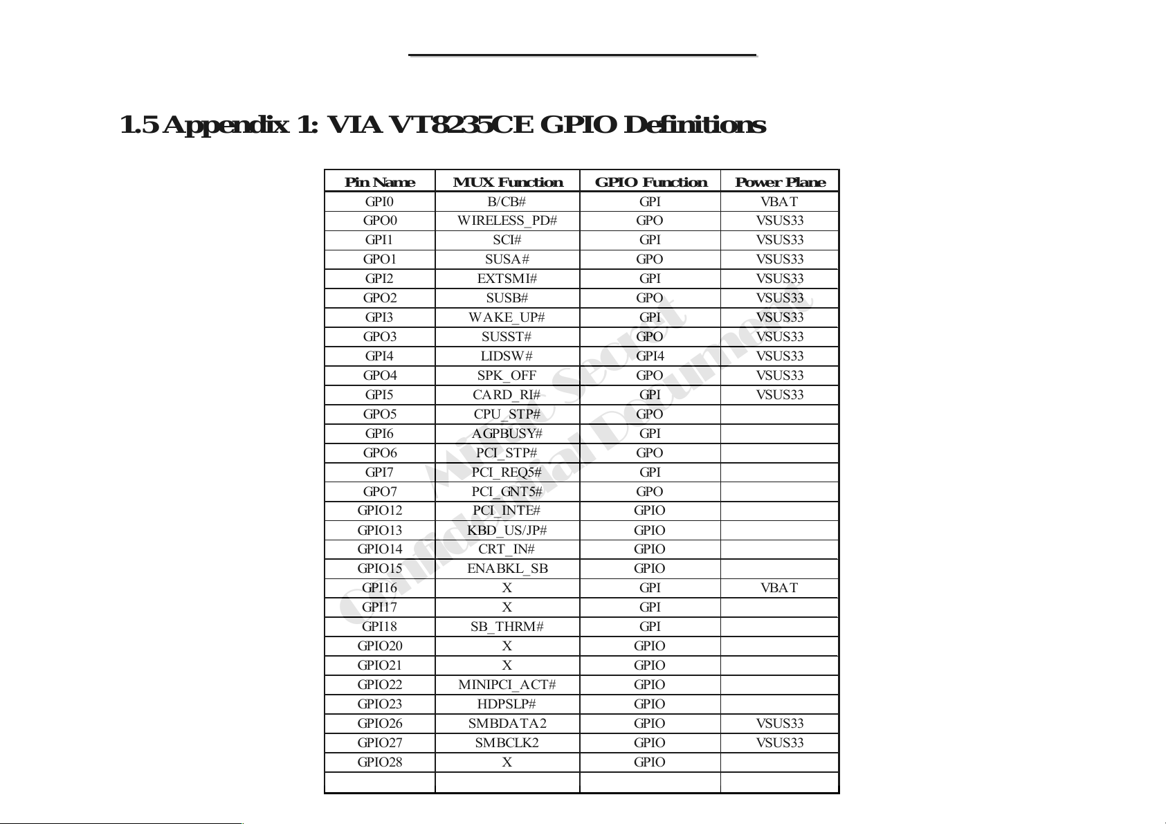
1.5 Appendix 1: VIA VT8235CE GPIO Definitions
Pin Name MUX Func t i on GPIO Function Power Plane
GP I0 B/ C B# GP I VBA T
GPO0 WIRELESS_PD# GPO VSUS33
GPI1 SCI# GPI VSUS33
GPO1 SUSA# GPO VSUS33
GP I2 EX TS M I# GPI VS US 33
GPO2 SUSB# GPO VSUS33
GP I3 W A K E_ UP # GPI VS US 33
GPO3 SUSST# GPO VSUS33
GP I4 L ID SW # GP I4 VS US 33
GPO4 SPK_OFF GPO VSUS33
GPI5 CARD_ RI# GPI VSUS33
GPO5 CPU_STP# GPO
GP I6 A GP BU SY# GP I
GPO6 PCI_STP# GPO
GPI7 PCI_REQ5# GPI
GP O7 P CI_ GN T 5# GPO
GPIO12 PCI_INTE# GPIO
GPIO13 KBD_US/JP# GPIO
GP IO 14 CRT _ I N# GP IO
GP IO 15 EN A BK L_ S B GP I O
GP I1 6 X GP I VBA T
GP I1 7 X GP I
Confidential Document
GPI18 SB_THRM# GPI
GP IO 20 X GP IO
GP IO 21 X GP IO
GPIO22 MINIPCI_ACT# GPIO
GP IO 23 HDP SLP # GP IO
GP IO 26 S M BDA T A 2 GP IO VSUS 3 3
GPIO27 SMBCLK2 GPIO VSUS33
GP IO 28 X GP IO
GP IO 29 DP RS LPVR GP IO
MiTac Secret
47
Page 49
8666 N/B Maintenance
8666 N/B Maintenance
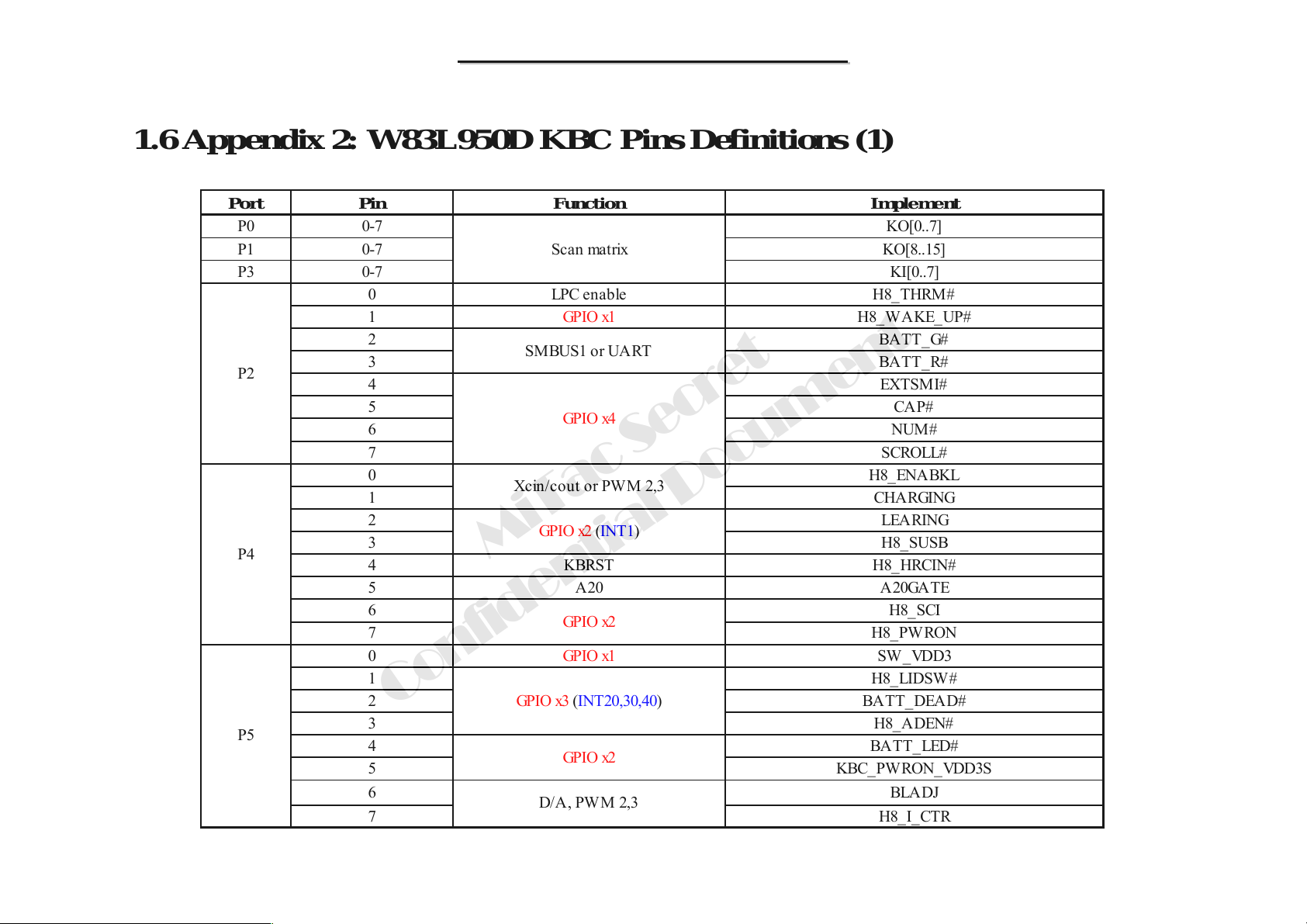
1.6 Appendix 2: W83L950D KBC Pins Definitions (1)
Port Pin Function Implement
P0 0-7 KO[0..7]
P1 0-7 KO[8..15]
P3 0-7 KI[0..7]
0 LPC enable H8_THRM#
1 GPIO x1 H8_WA KE_UP#
2 BATT_G#
P2
P4
P5
3 BATT_R#
4EXTSMI#
5CAP#
6 NUM#
7 SCROLL#
0H8_ENABKL
1CHARGING
2LEARING
3 H8_SUSB
4 KBRST H8_HRCIN#
5 A20 A20GATE
6H8_SCI
7H8_PWRON
0 GPIO x1 SW_VDD3
1H8_LIDSW#
2 BATT_DEAD#
Confidential Document
3H8_ADEN#
4 BATT_LED#
5 KBC_PWRON_VDD3S
6BLADJ
7H8_I_CTR
MiTac Secret
Scan matrix
SMBUS1 or UART
GPIO x4
Xcin/cout or PWM 2,3
GPIO x2 (INT1)
GPIO x2
GPIO x3 (INT20,30,40)
GPIO x2
D/A, PW M 2,3
48
Page 50
8666 N/B Maintenance
8666 N/B Maintenance
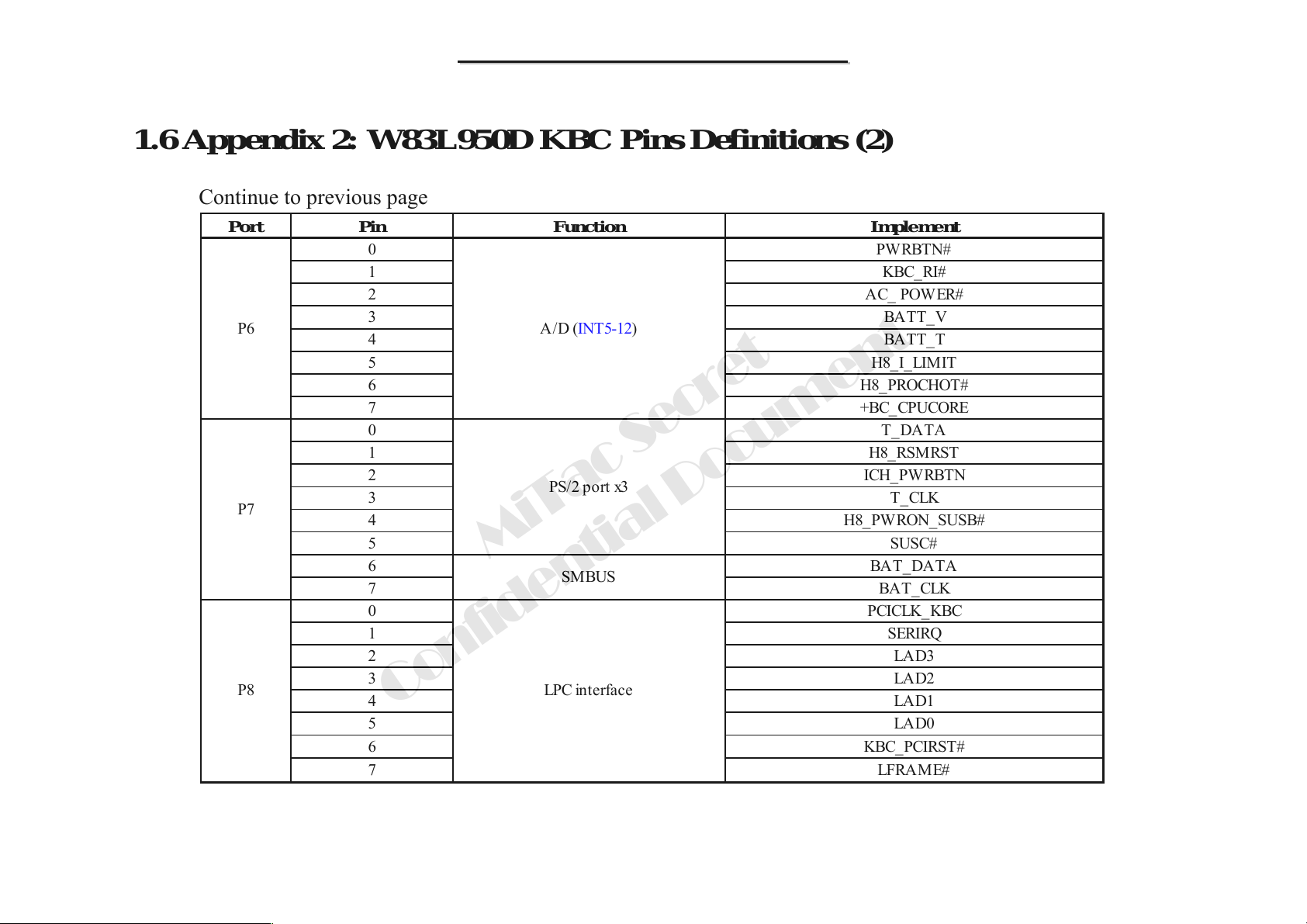
1.6 Appendix 2: W83L950D KBC Pins Definitions (2)
Continue to previous page
Port Pin Function Implement
0 PWRBTN#
1 KBC_RI#
2 AC_ POWER#
P6 A/D (INT5-12)
P7
P8 LPC interface
3 BATT_V
4 BATT_T
5H8_I_LIMIT
6H8_PROCHOT#
7 +BC_CPUCORE
0T_DATA
1H8_RSMRST
2 ICH_ PWRBTN
3T_CLK
4 H8_PWRON_SUSB#
5SUSC#
6 BAT_DATA
7BAT_CLK
0 PCICLK_KBC
1SERIRQ
2LAD3
3LAD2
4LAD1
Confidential Document
5LAD0
6 KBC_PCIRST#
7LFRAME#
MiTac Secret
PS/2 port x3
SMBUS
49
Page 51
8666 N/B Maintenance
8666 N/B Maintenance
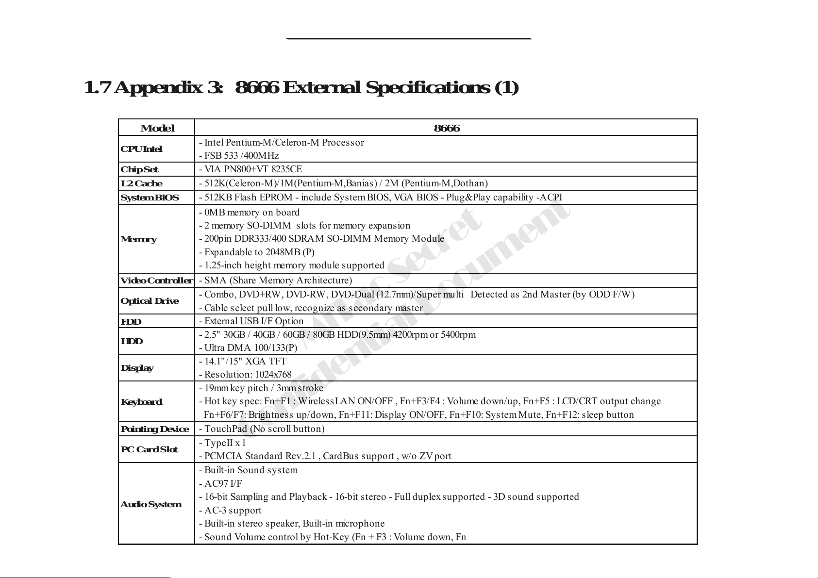
1.7 Appendix 3: 8666 External Specifications (1)
Model 8666
CPU Intel
Chip Set
L2 Cache
Syste m BIOS
Memory
Video Co ntro ller
Optic al Drive
FDD
HDD
Disp lay
Keyb oard
Point ing Device
PC Card Slot
Aud io System
- Intel Pentium-M/Celeron-M Proces sor
- FSB 533 /400MHz
- VIA PN800+VT 8235CE
- 512K(Celeron-M)/1M(Pentium-M,Banias) / 2M (Pentium-M,Dothan)
- 512KB Flash EPROM - include System BIOS, VGA BIOS - Plug&Play capability -ACPI
- 0MB memory on board
- 2 memory SO-DIMM slots for memory expansion
- 200pin DDR333/400 SDRAM SO-DIMM Memory Module
- Expandable to 2048MB (P)
- 1.25-inch height memory module supported
- SMA (Share Memory Architecture)
- Combo, DVD+RW, DVD-RW, DVD-Dual (12.7mm)/Super multi Detected as 2nd Mas ter (by ODD F/W)
- Cable select pull low, recognize as secondary master
- External USB I/F Option
- 2.5" 30GB / 40GB / 60GB / 80GB HDD(9.5mm) 4200rpm or 5400rpm
- Ultra DMA 100/133(P)
- 14.1" /15" XGA TFT
- Resolutio n: 1024x768
- 19mm key pitch / 3mm stroke
- Hot key spec: Fn+F1 : WirelessLAN ON/OFF , Fn+F3/F4 : Volume down/up, Fn+F5 : LCD/CRT output change
Fn+F6/F7: Brightness up/down, Fn+F11: Display ON/OFF, Fn+F10: System Mute, Fn+F12: sleep button
- TouchPad (No scroll button)
- TypeII x 1
- PCMCIA Standard Rev.2.1 , CardBus support , w/o ZV port
- Built-in Sound system
- AC97 I/F
- 16-bit Sampling and Playback - 16-bit stereo - Full duplex supported - 3D sound supported
- AC-3 support
- Built-in stereo speaker, Built-in microphone
- Sound Volume control by Hot-Key (Fn + F3 : Volume down, Fn
Confidential Document
MiTac Secret
50
Page 52
8666 N/B Maintenance
8666 N/B Maintenance
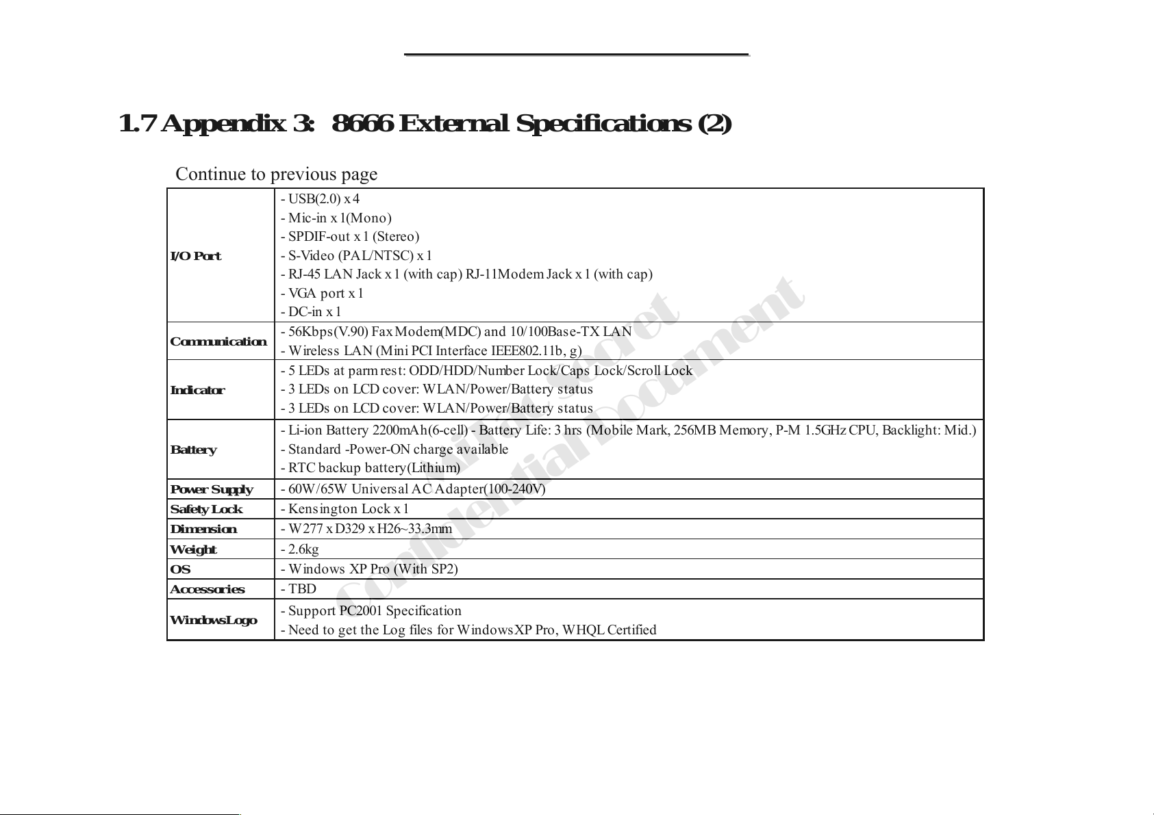
1.7 Appendix 3: 8666 External Specifications (2)
Continue to previous page
- USB(2.0) x 4
- Mic-in x 1(Mono)
- SPDIF-out x 1 (Stereo)
I/O Port
Com munication
Indicator
Battery
Power Supply
Safet y Loc k
Dimension
Weig ht
OS
Accessories
WindowsLogo
- S-Video (PAL/NTSC) x 1
- RJ-45 LAN Jack x 1 (with cap ) RJ-11M odem Jack x 1 (with cap)
- VGA port x 1
- DC-in x 1
- 56Kbps(V.90) Fax Modem(MDC) and 10/100Base-TX LAN
- W ireles s LAN (Mini PCI In terface IEEE802.11b , g)
- 5 LEDs at parm rest: ODD/HDD/Number Lock/Caps Lock/Scroll Lock
- 3 LEDs on LCD cover: WLAN/Power/Battery status
- 3 LEDs on LCD cover: WLAN/Power/Battery status
- Li-ion Battery 2200mAh(6-cell) - Battery Life: 3 hrs (Mobile Mark, 256MB Memory, P-M 1.5GHz CPU, Backlight: Mid.)
- Standard -Power-ON charge available
- RTC backup battery(Lithium)
- 60W/65W Universal AC Adapter(100-240V)
- Kensington Lock x 1
- W277 x D329 x H26~33.3mm
- 2.6kg
- Windows XP Pro (With SP2)
- TBD
- Su pport PC2001 Specificat ion
- Need to get the Log files for WindowsXP Pro, WHQL Certified
Confidential Document
MiTac Secret
51
Page 53
8666 N/B Maintenance
8666 N/B Maintenance
2. System View and Disassembly
2.1 System View
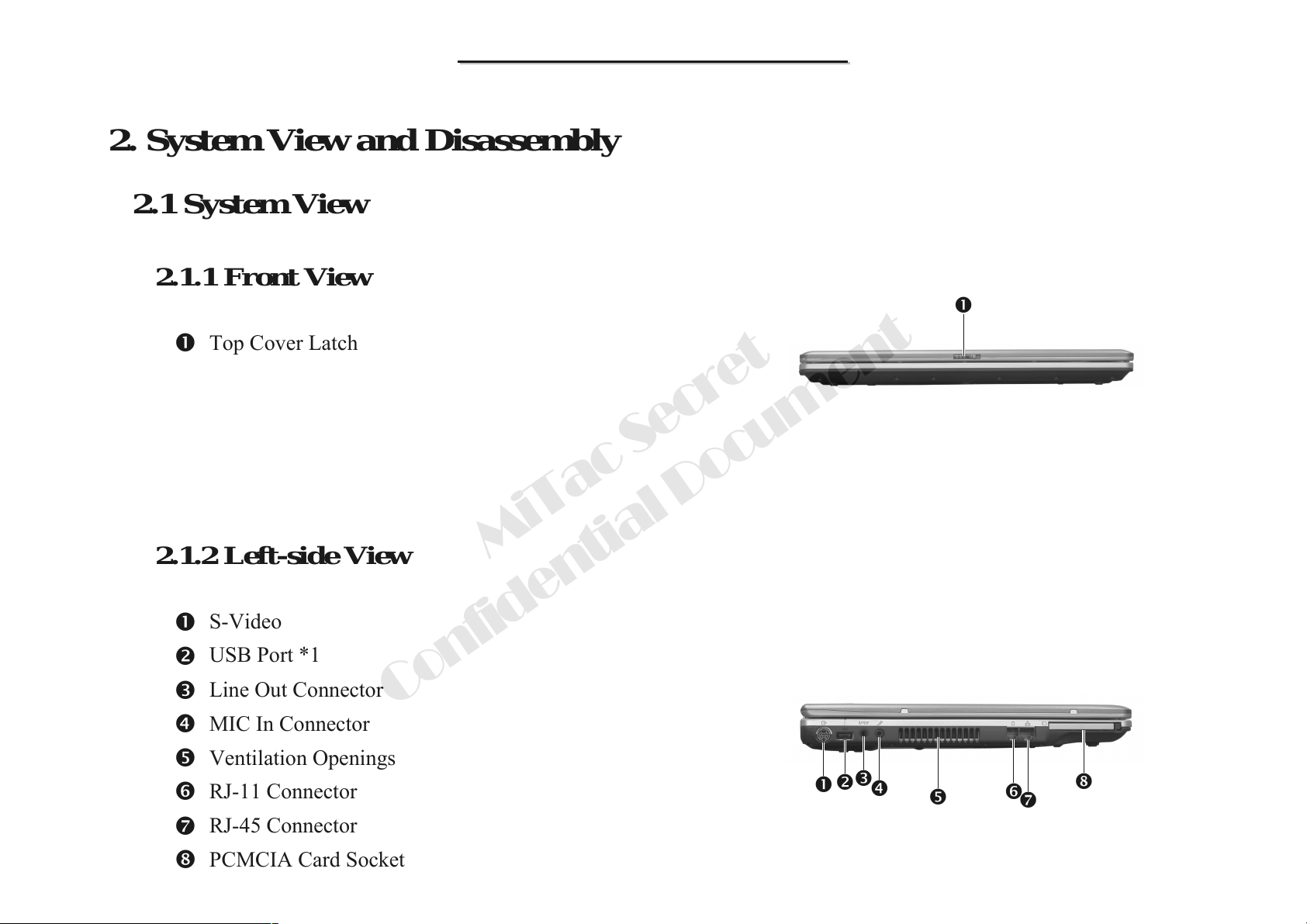
2.1.1 Front View
Top Cover Latch
2.1.2 Left-side View
S-Video
USB Port *1
Line Out Connector
MIC In Connector
Ventilation Openings
RJ-11 Connector
RJ-45 Connector
PCMCIA Card Socket
Confidential Document
MiTac Secret
52
Page 54
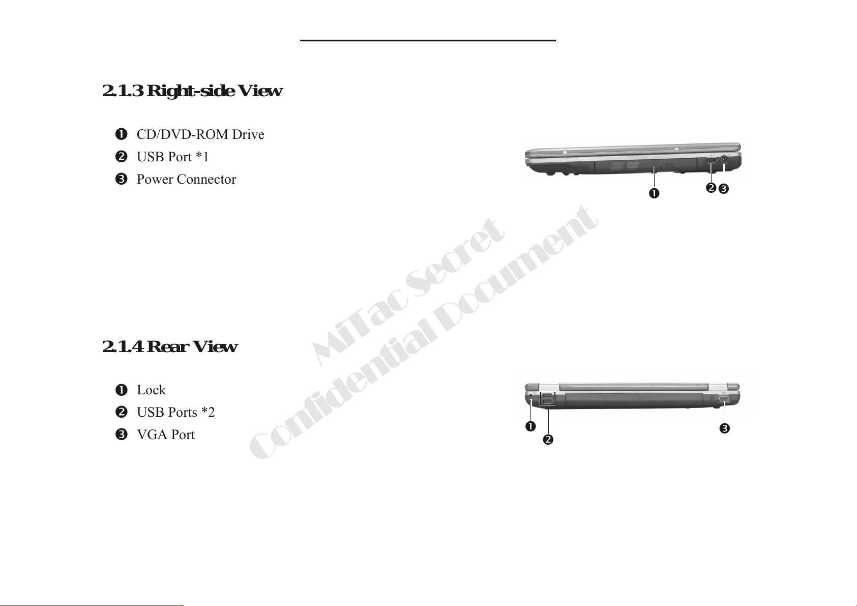
2.1.3 Right-side View
CD/DVD-ROM Drive
USB Port *1
Power Connector
8666 N/B Maintenance
8666 N/B Maintenance
2.1.4 Rear View
Lock
USB Ports *2
VGA Port
MiTac Secret
Confidential Document
53
Page 55
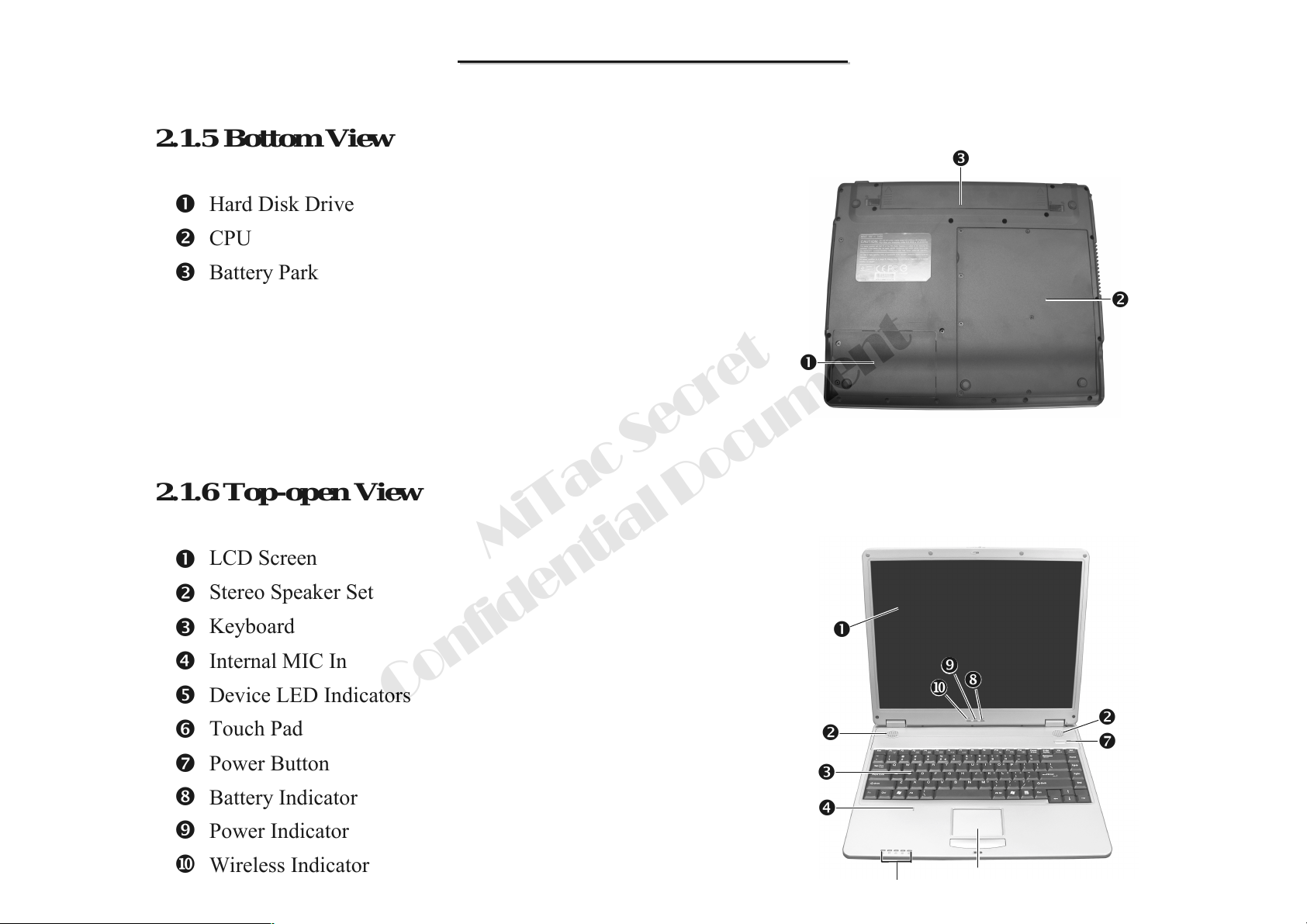
2.1.5 Bottom View
Hard Disk Drive
CPU
Battery Park
2.1.6 Top-open View
8666 N/B Maintenance
8666 N/B Maintenance
LCD Screen
Stereo Speaker Set
Keyboard
Internal MIC In
Device LED Indicators
Touch Pad
Power Button
Battery Indicator
Power Indicator
Wireless Indicator
MiTac Secret
Confidential Document
54
Page 56
8666 N/B Maintenance
8666 N/B Maintenance
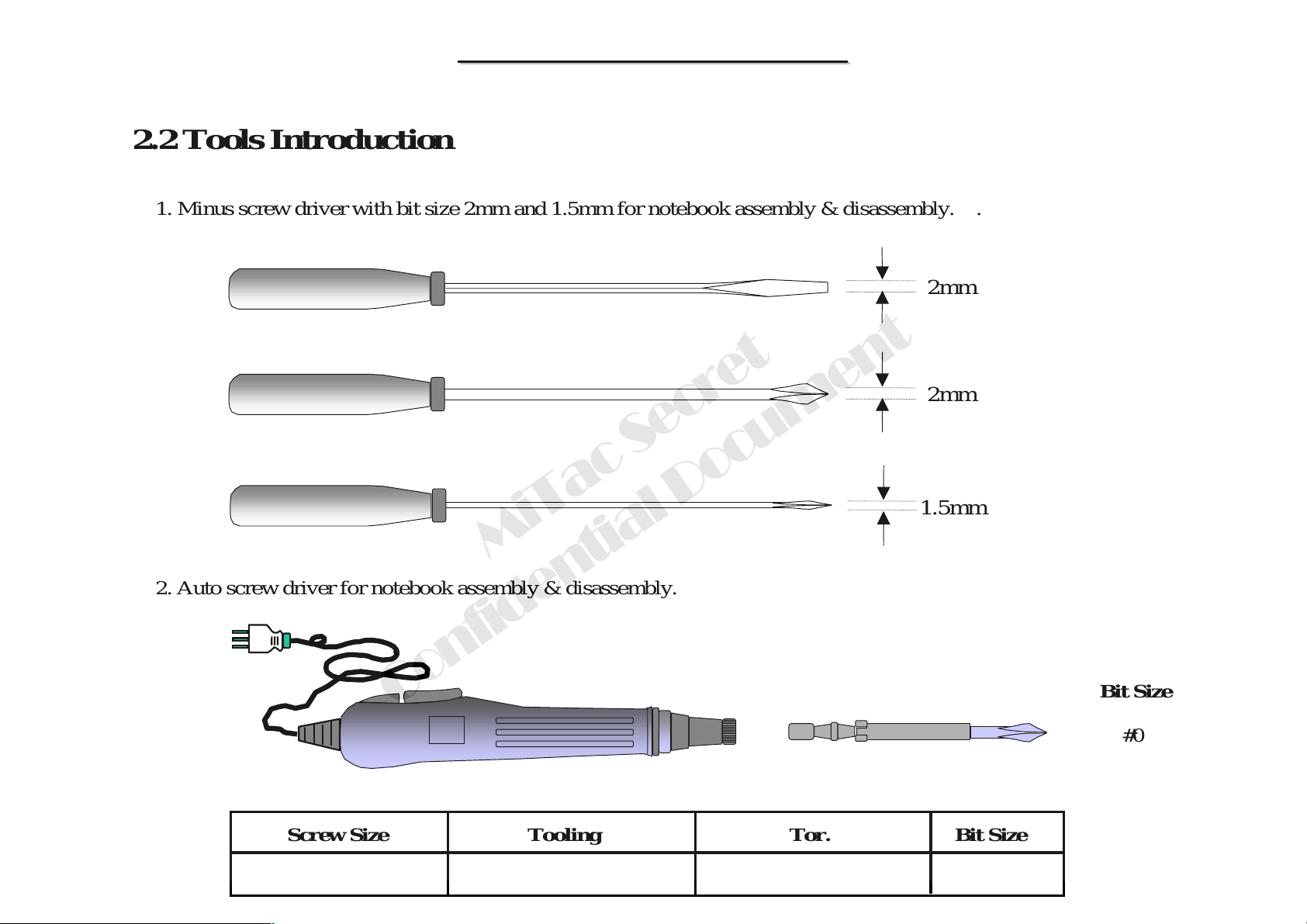
2.2 Tools Introduction
1. Minus screw driv e r with bit size 2mm and 1.5mm for notebook assembly & disassembly. .
2mm
2mm
MiTac Secret
2. Auto screw driver for notebook assembly & disassembly.
Confidential Document
Screw Size Tooling Tor. Bit Size
1. M2.0 Auto-Screw driver 2.0-2.5 kg/cm2 #0
1.5mm
Bit Size
#0
55
Page 57
8666 N/B Maintenance
8666 N/B Maintenance
2.3 System Disassembly
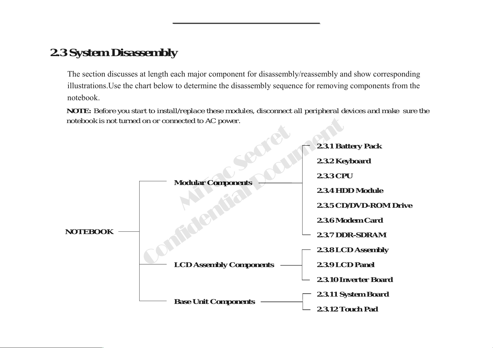
The section discusses at length each major component for disassembly/reassembly and show corresponding
illustrations.Use the chart below to determine the disassembly sequence for removing components from the
notebook.
NOTE: Before you start to install/replace these modules, disconnect all peripheral devices and make sure the
notebook is not turned on or connected to AC power.
2.3.1 Battery Pack
2.3.2 Keyboard
2.3.3 CPU
Modular Components
2.3.4 HDD Module
NOTEBOOK
MiTac Secret
Confidential Document
LCD Assembly Components
Base Unit Components
2.3.5 CD/DVD-ROM Drive
2.3.6 Modem Card
2.3.7 DDR-SDRAM
2.3.8 LCD Assem bly
2.3.9 LCD Panel
2.3.10 Inverter Board
2.3.11 System Board
2.3.12 Touch Pad
56
Page 58
8666 N/B Maintenance
8666 N/B Maintenance
2.3.1 Battery Pack
Disassembly
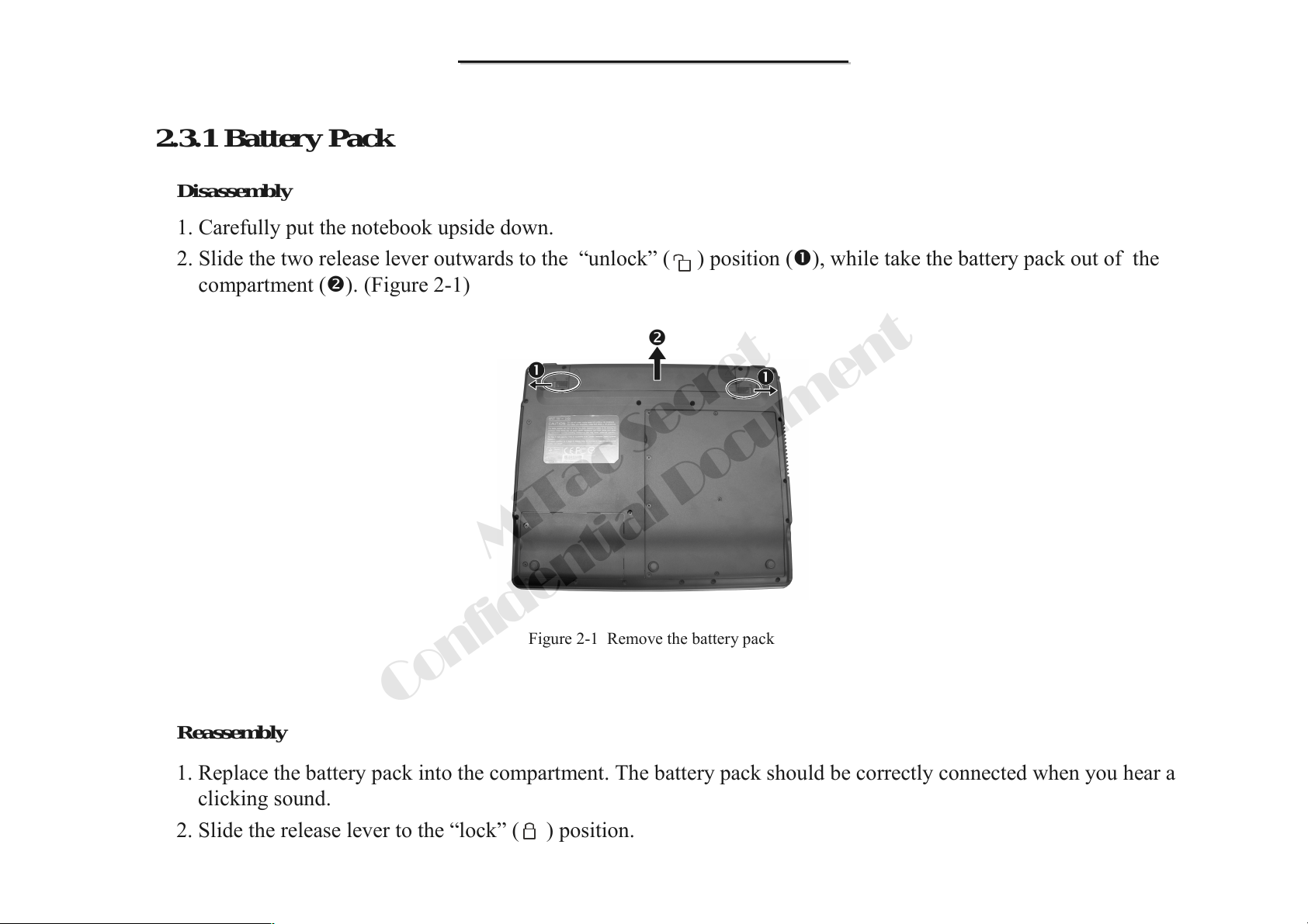
1. Carefully put the notebook upside down.
2. Slide the two release lever outwards to the “unlock” ( ) position (), while take the battery pack out of the
compartment (). (Figure 2-1)
MiTac Secret
Figure 2-1 Remove the battery pack
Confidential Document
Reassembly
1. Replace the battery pack into the compartment. The battery pack should be correctly connected when you hear a
clicking sound.
2. Slide the release lever to the “lock” ( ) position.
57
Page 59
8666 N/B Maintenance
8666 N/B Maintenance
2.3.2 Keyboard
Disassembly
1. Remove the battery pack. (Refer to section 2.3.1 Disassembly)
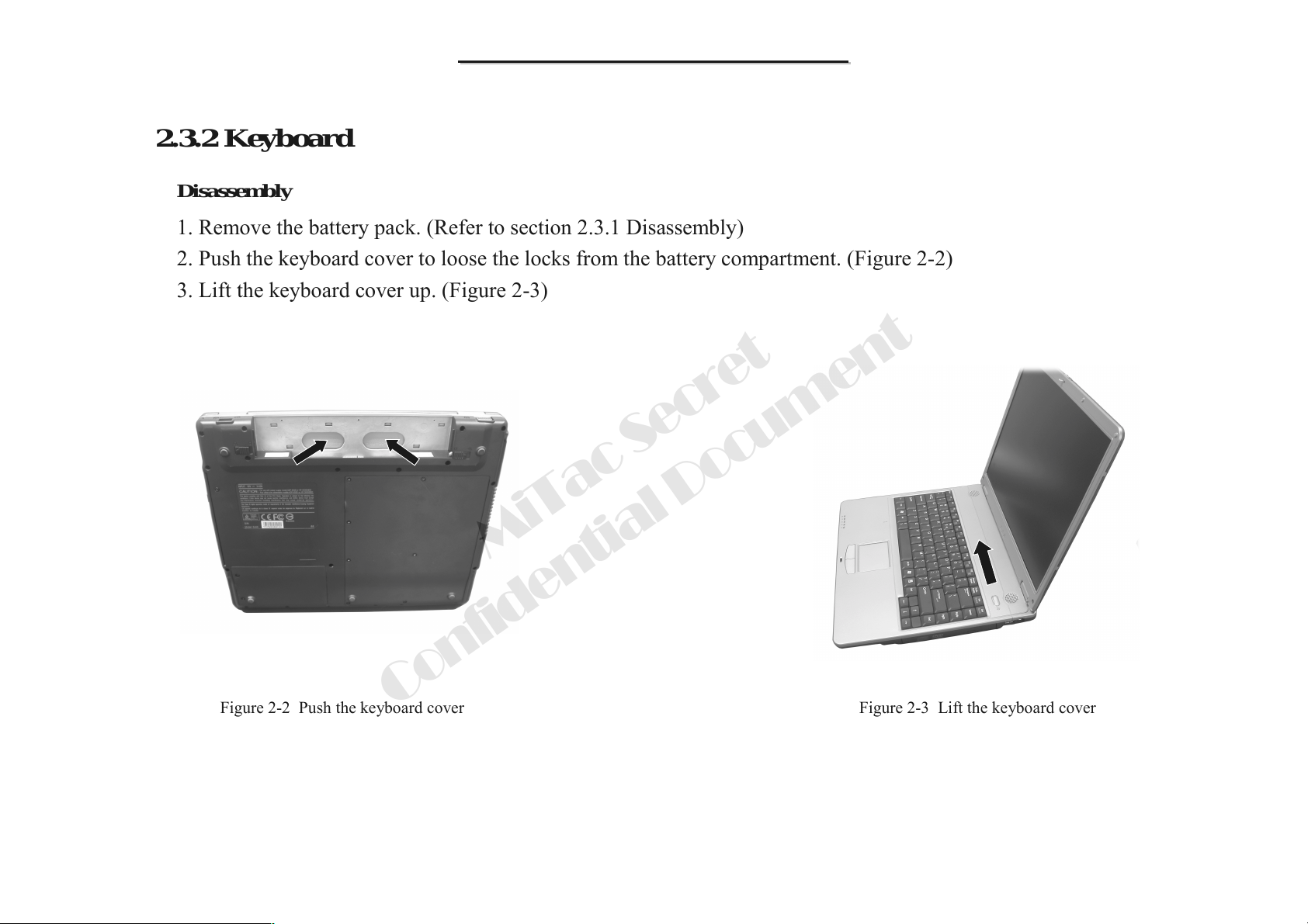
2. Push the keyboard cover to loose the locks from the battery compartment. (Figure 2-2)
3. Lift the keyboard cover up. (Figure 2-3)
MiTac Secret
Figure 2-2 Push the keyboard cover Figure 2-3 Lift the keyboard cover
Confidential Document
58
Page 60
8666 N/B Maintenance
8666 N/B Maintenance
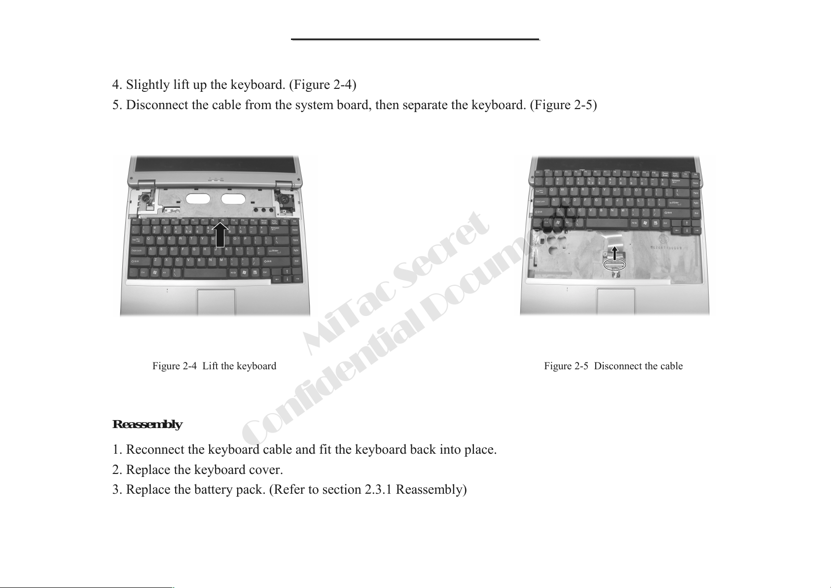
4. Slightly lift up the keyboard. (Figure 2-4)
5. Disconnect the cable from the system board, then separate the keyboard. (Figure 2-5)
MiTac Secret
Figure 2-4 Lift the keyboard Figure 2-5 Disconnect the cable
Reassembly
1. Reconnect the keyboard cable and fit the keyboard back into place.
2. Replace the keyboard cover.
3. Replace the battery pack. (Refer to section 2.3.1 Reassembly)
Confidential Document
59
Page 61
8666 N/B Maintenance
8666 N/B Maintenance
2.3.3 CPU
Disassembly
1. Remove the battery pack. (Refer to section 2.3.1 Disassembly)
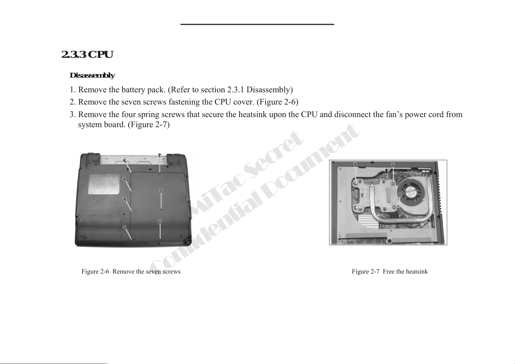
2. Remove the seven screws fastening the CPU cover. (Figure 2-6)
3. Remove the four spring screws that secure the heatsink upon the CPU and disconnect the fan’s power cord from
system board. (Figure 2-7)
Figure 2-6 Remove the seven screws
Confidential Document
MiTac Secret
Figure 2-7 Free the heatsink
60
Page 62
8666 N/B Maintenance
8666 N/B Maintenance
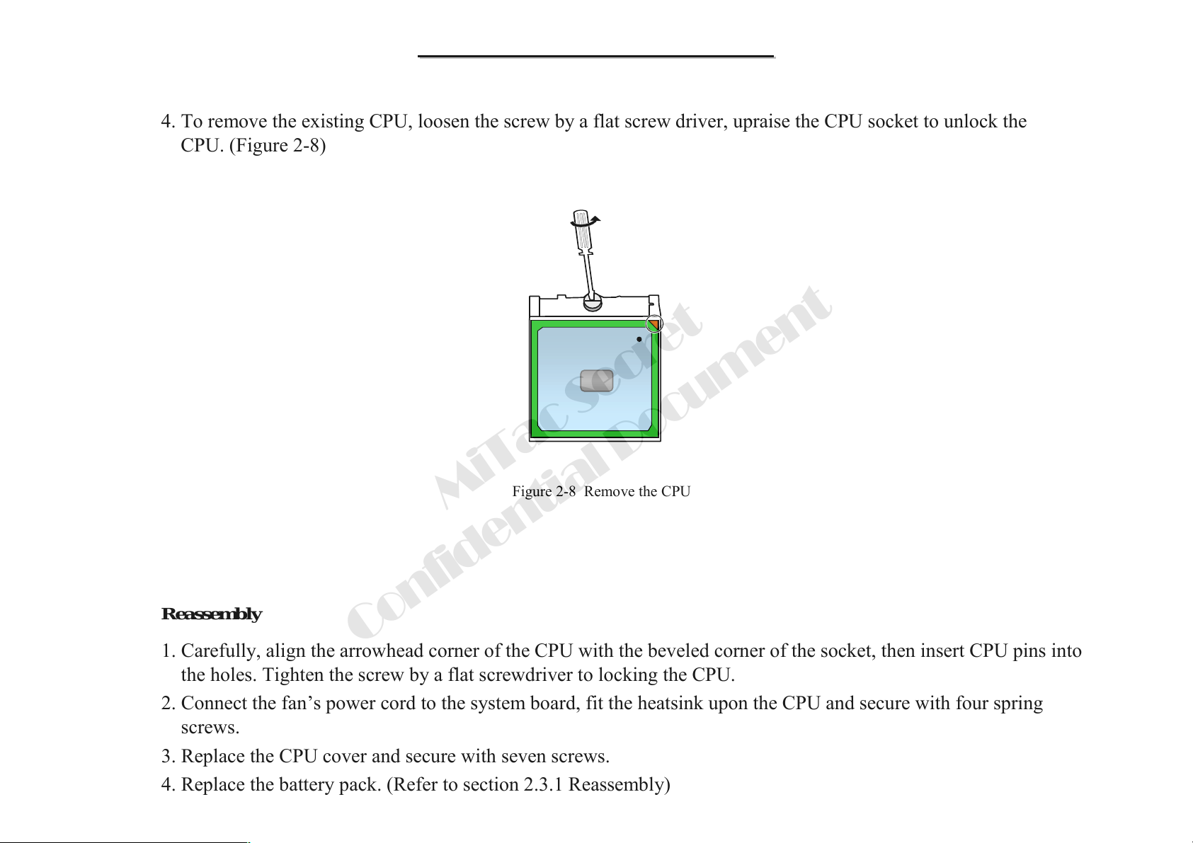
4. To remove the existing CPU, loosen the screw by a flat screw driver, upraise the CPU socket to unlock the
CPU. (Figure 2-8)
MiTac Secret
Figure 2-8 Remove the CPU
Reassembly
Confidential Document
1. Carefully, align the arrowhead corner of the CPU with the beveled corner of the socket, then insert CPU pins into
the holes. Tighten the screw by a flat screwdriver to locking the CPU.
2. Connect the fan’s power cord to the system board, fit the heatsink upon the CPU and secure with four spring
screws.
3. Replace the CPU cover and secure with seven screws.
4. Replace the battery pack. (Refer to section 2.3.1 Reassembly)
61
Page 63
8666 N/B Maintenance
8666 N/B Maintenance
2.3.4 HDD Module
Disassembly
1. Carefully put the notebook upside down. Remove the battery pack. (Refer to section 2.3.1 Disassembly)
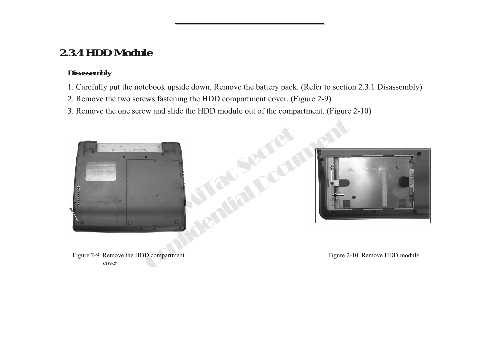
2. Remove the two screws fastening the HDD compartment cover. (Figure 2-9)
3. Remove the one screw and slide the HDD module out of the compartment. (Figure 2-10)
cover
MiTac Secret
Figure 2-10 Remove HDD moduleFigure 2-9 Remove the HDD compartment
Confidential Document
62
Page 64
8666 N/B Maintenance
8666 N/B Maintenance
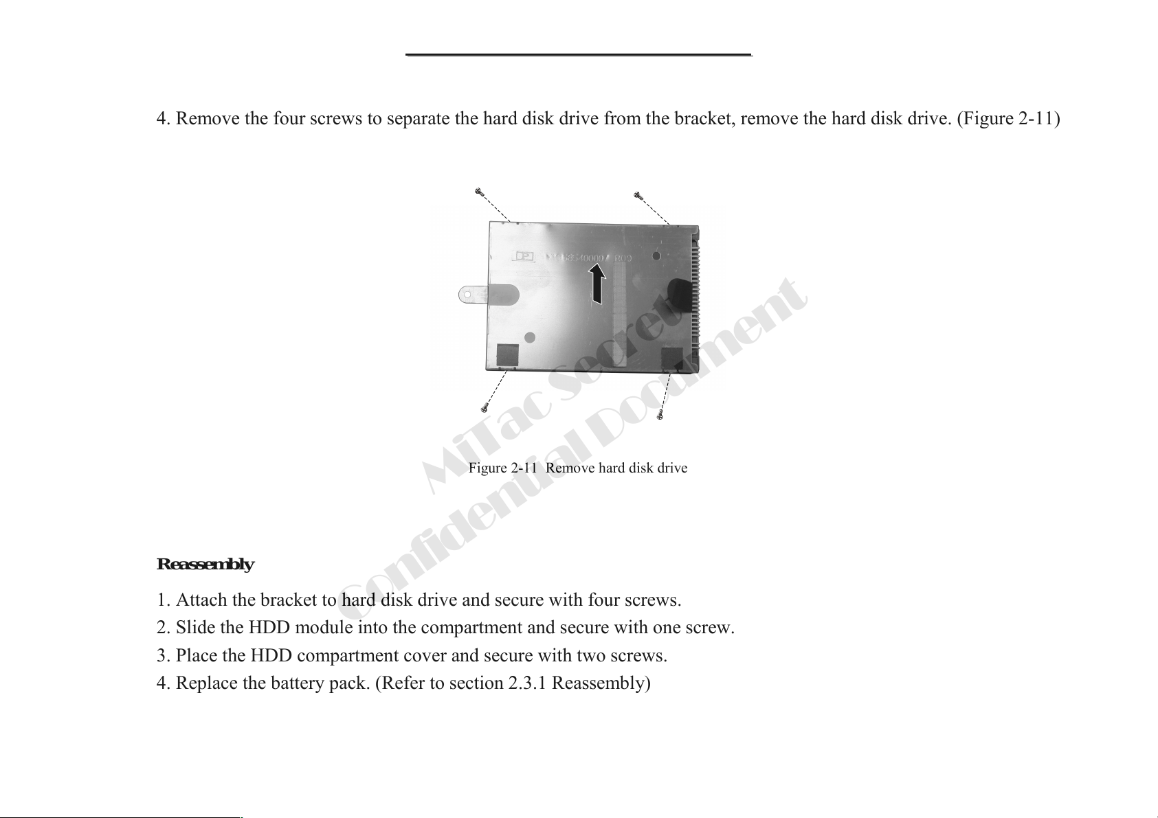
4. Remove the four screws to separate the hard disk drive from the bracket, remove the hard disk drive. (Figure 2-11)
Figure 2-11 Remove hard disk drive
MiTac Secret
Reassembly
1. Attach the bracket to hard disk drive and secure with four screws.
2. Slide the HDD module into the compartment and secure with one screw.
3. Place the HDD compartment cover and secure with two screws.
4. Replace the battery pack. (Refer to section 2.3.1 Reassembly)
Confidential Document
63
Page 65

8666 N/B Maintenance
8666 N/B Maintenance
2.3.5 CD/DVD-ROM Drive
Disassembly
1. Carefully put the notebook upside down. Remove the battery pack. (Refer to section 2.3.1 Disassembly)
2. Remove the one screw fastening the CD/DVD-ROM drive. (Figure 2-12)
3. Insert a small rod, such as a straightened paper clip, into CD/DVD-ROM drive’s manual eject hole () and push
firmly to release the tray. Then gently pull out the CD/DVD-ROM drive by holding the tray that pops out ().
(Figure 2-12)
MiTac Secret
Confidential Document
Reassembly
1. Push the CD/DVD-ROM drive into the compartment and secure with one screw.
2. Replace the battery pack. (Refer to section 2.3.1 Reassembly)
Figure 2-12 Remove the CD/DVD-ROM drive
64
Page 66
8666 N/B Maintenance
8666 N/B Maintenance
2.3.6 Modem Card
Disassembly
1. Carefully put the notebook upside down. Remove the battery pack. (Refer to section 2.3.1 Disassembly)
2. Remove the seven screws fastening the CPU cover. (Refer to step 2 of section 2.3.3 Disassembly)
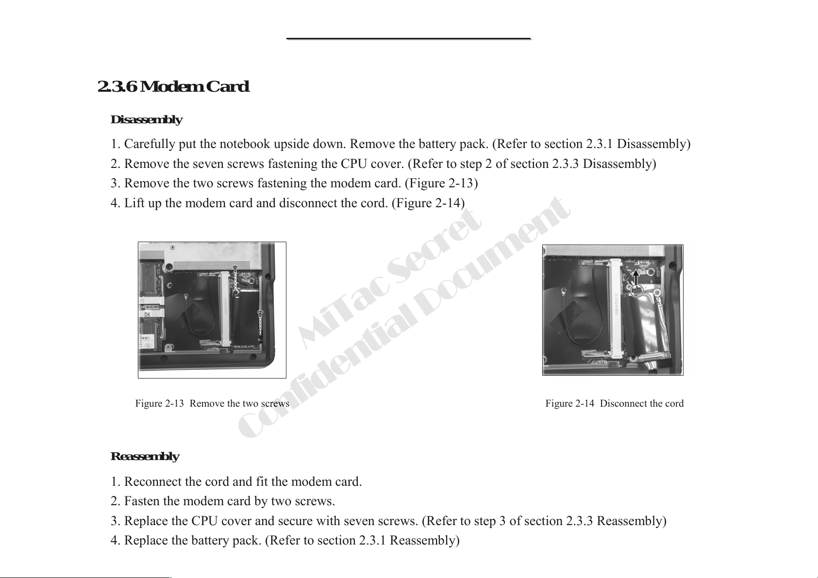
3. Remove the two screws fastening the modem card. (Figure 2-13)
4. Lift up the modem card and disconnect the cord. (Figure 2-14)
MiTac Secret
Figure 2-13 Remove the two screws Figure 2-14 Disconnect the cord
Confidential Document
Reassembly
1. Reconnect the cord and fit the modem card.
2. Fasten the modem card by two screws.
3. Replace the CPU cover and secure with seven screws. (Refer to step 3 of section 2.3.3 Reassembly)
4. Replace the battery pack. (Refer to section 2.3.1 Reassembly)
65
Page 67
8666 N/B Maintenance
8666 N/B Maintenance
2.3.7 DDR-SDRAM
Disassembly
1. Carefully put the notebook upside down. Remove the battery pack. (See section 2.3.1 Disassembly)
2. Remove the seven screws fastening the CPU cover. (Refer to step 2 of section 2.3.3 Disassembly)
MiTac Secret
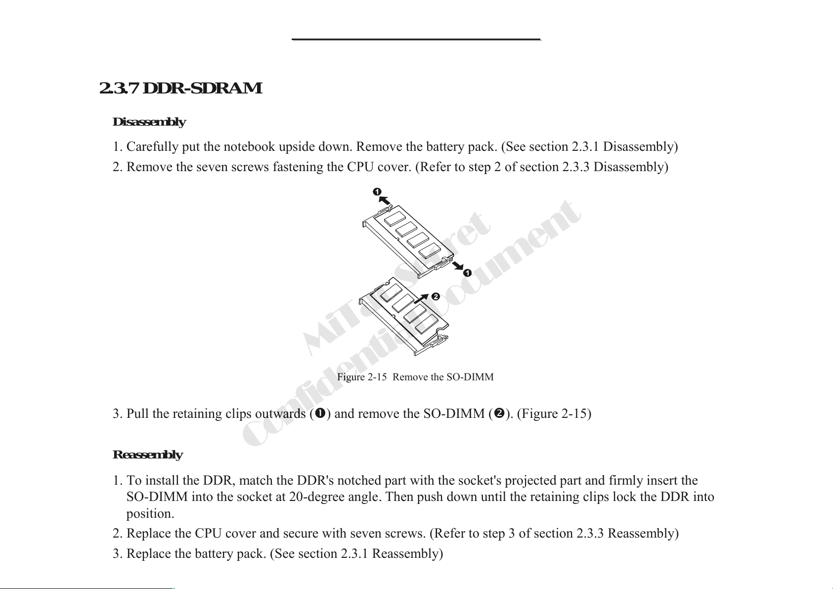
Figure 2-15 Remove the SO-DIMM
3. Pull the retaining clips outwards () and remove the SO-DIMM (). (Figure 2-15)
Reassembly
1. To install the DDR, match the DDR's notched part with the socket's projected part and firmly insert the
SO-DIMM into the socket at 20-degree angle. Then push down until the retaining clips lock the DDR into
position.
2. Replace the CPU cover and secure with seven screws. (Refer to step 3 of section 2.3.3 Reassembly)
3. Replace the battery pack. (See section 2.3.1 Reassembly)
Confidential Document
66
Page 68
8666 N/B Maintenance
8666 N/B Maintenance
2.3.8 LCD ASSY
Disassembly
1. Remove the battery pack and keyboard. (See sections 2.3.1 and 2.3.2 Disassembly)
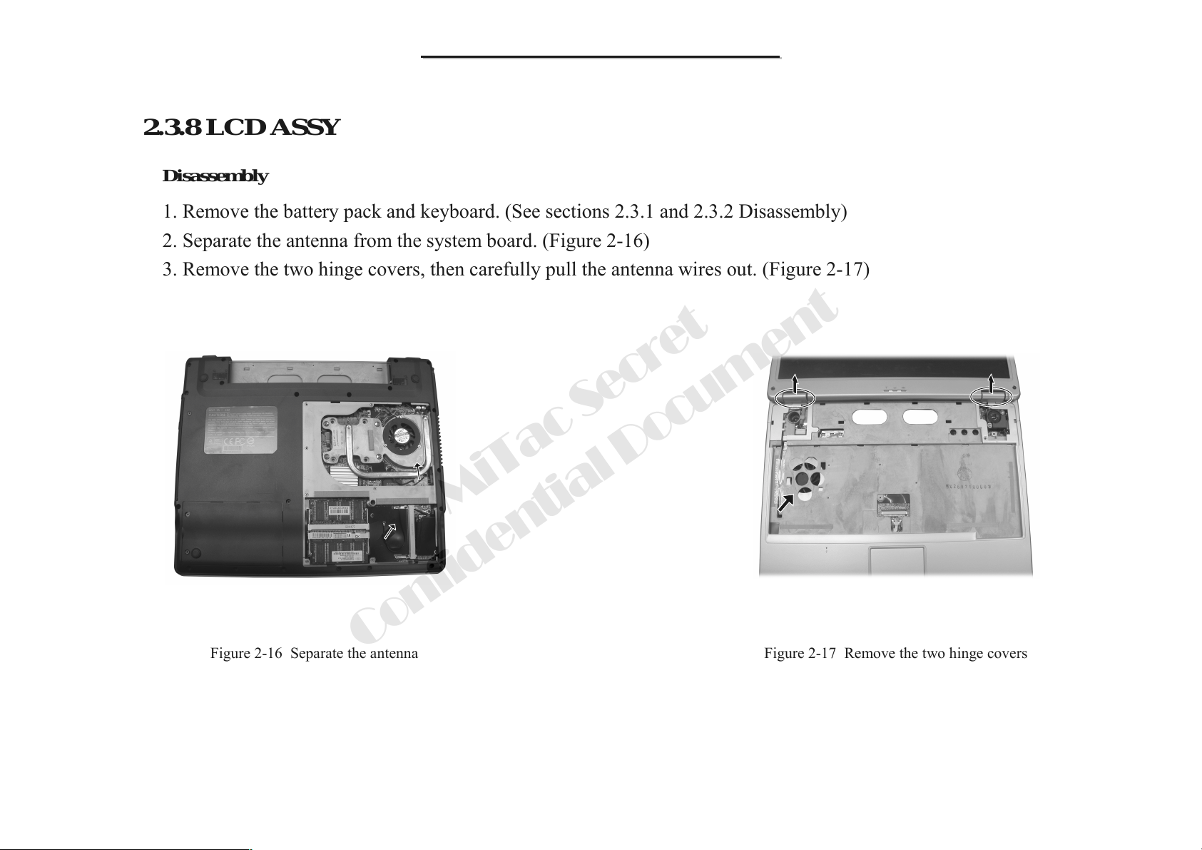
2. Separate the antenna from the system board. (Figure 2-16)
3. Remove the two hinge covers, then carefully pull the antenna wires out. (Figure 2-17)
MiTac Secret
Figure 2-16 Separate the antenna Figure 2-17 Remove the two hinge covers
Confidential Document
67
Page 69
8666 N/B Maintenance
8666 N/B Maintenance
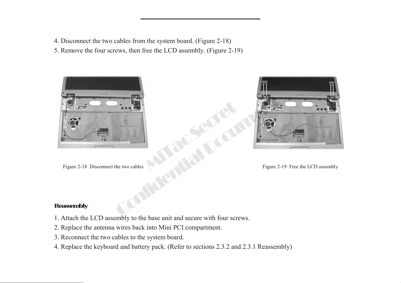
4. Disconnect the two cables from the system board. (Figure 2-18)
5. Remove the four screws, then free the LCD assembly. (Figure 2-19)
Figure 2-18 Disconnect the two cables Figure 2-19 Free the LCD assembly
Reassembly
1. Attach the LCD assembly to the base unit and secure with four screws.
2. Replace the antenna wires back into Mini PCI compartment.
3. Reconnect the two cables to the system board.
4. Replace the keyboard and battery pack. (Refer to sections 2.3.2 and 2.3.1 Reassembly)
Confidential Document
MiTac Secret
68
Page 70
8666 N/B Maintenance
8666 N/B Maintenance
2.3.9 LCD Panel
Disassembly
1. Remove the battery, keyboard and LCD assembly. (Refer to section 2.3.1, 2.3.2 and 2.3.8 Disassembly)
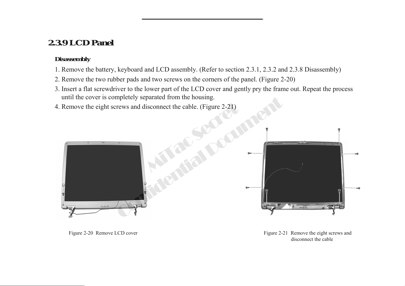
2. Remove the two rubber pads and two screws on the corners of the panel. (Figure 2-20)
3. Insert a flat screwdriver to the lower part of the LCD cover and gently pry the frame out. Repeat the process
until the cover is completely separated from the housing.
4. Remove the eight screws and disconnect the cable. (Figure 2-21)
Confidential Document
Figure 2-20 Remove LCD cover
MiTac Secret
Figure 2-21 Remove the eight screws and
disconnect the cable
69
Page 71
8666 N/B Maintenance
8666 N/B Maintenance
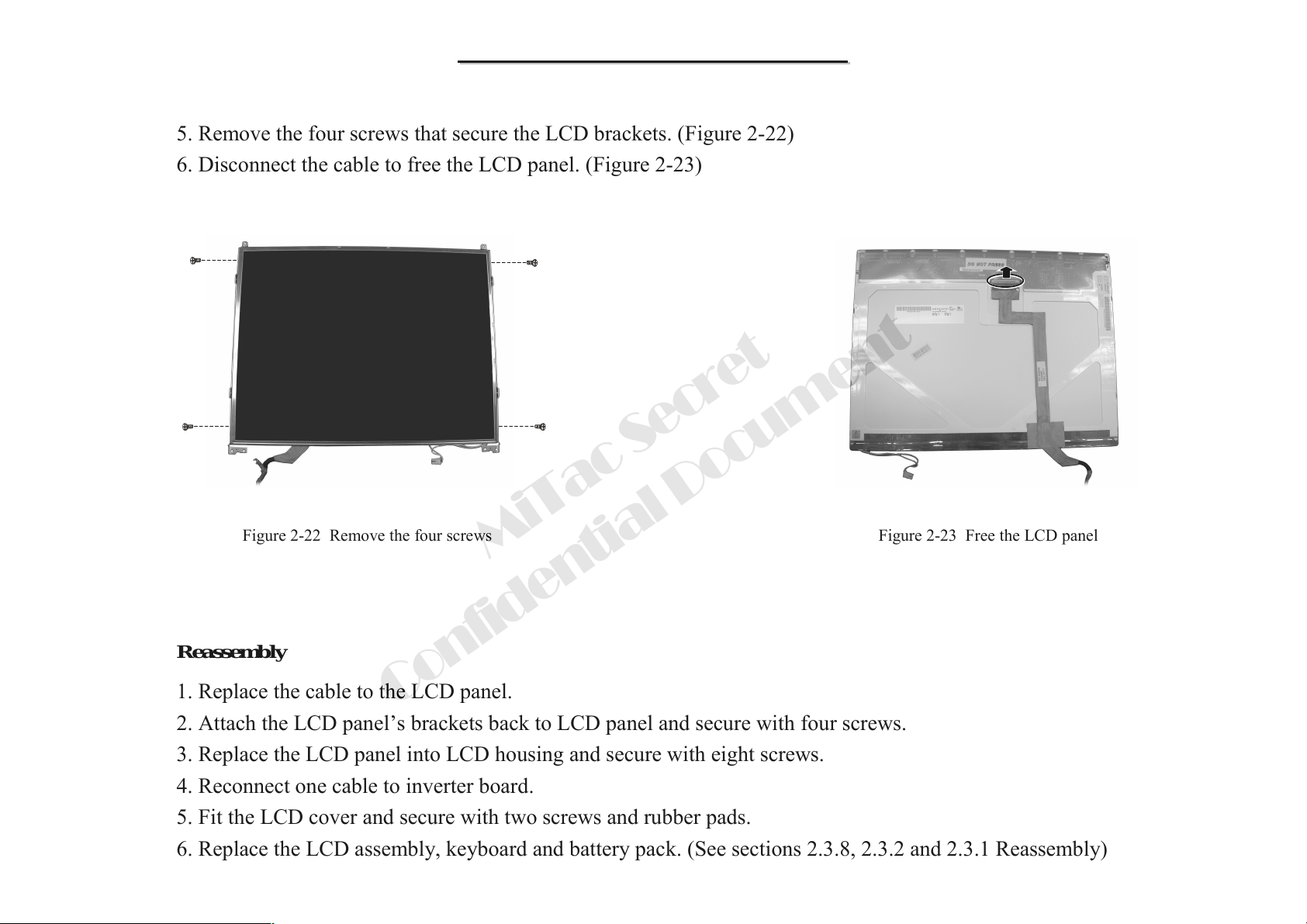
5. Remove the four screws that secure the LCD brackets. (Figure 2-22)
6. Disconnect the cable to free the LCD panel. (Figure 2-23)
Figure 2-22 Remove the four screws
Figure 2-23 Free the LCD panel
MiTac Secret
Reassembly
1. Replace the cable to the LCD panel.
2. Attach the LCD panel’s brackets back to LCD panel and secure with four screws.
3. Replace the LCD panel into LCD housing and secure with eight screws.
4. Reconnect one cable to inverter board.
5. Fit the LCD cover and secure with two screws and rubber pads.
6. Replace the LCD assembly, keyboard and battery pack. (See sections 2.3.8, 2.3.2 and 2.3.1 Reassembly)
Confidential Document
70
Page 72
8666 N/B Maintenance
8666 N/B Maintenance
2.3.10 Inverter Board
Disassembly
1. Remove the battery, keyboard and LCD assembly. (Refer to section 2.3.1, 2.3.2 and 2.3.8 Disassembly)
2. Remove the LCD cover. (Refer to the steps 1-3 of section 2.3.9 Disassembly )
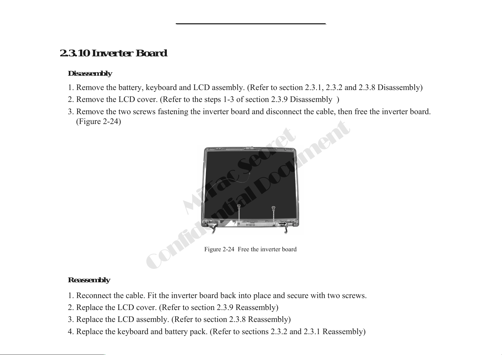
3. Remove the two screws fastening the inverter board and disconnect the cable, then free the inverter board.
(Figure 2-24)
MiTac Secret
Figure 2-24 Free the inverter board
Confidential Document
Reassembly
1. Reconnect the cable. Fit the inverter board back into place and secure with two screws.
2. Replace the LCD cover. (Refer to section 2.3.9 Reassembly)
3. Replace the LCD assembly. (Refer to section 2.3.8 Reassembly)
4. Replace the keyboard and battery pack. (Refer to sections 2.3.2 and 2.3.1 Reassembly)
71
Page 73
8666 N/B Maintenance
8666 N/B Maintenance
2.3.11 System Board
Disassembly
1. Remove the battery, keyboard, CPU, hard disk drive, CD/DVD-ROM drive, modem card, DDR and LCD
assembly. (Refer to sections 2.3.1, 2.3.2, 2.3.3, 2.3.4, 2.3.5, 2.3.6, 2.3.7 and 2.3.8 Disassembly)
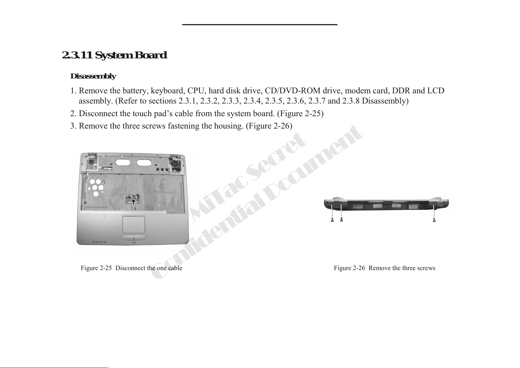
2. Disconnect the touch pad’s cable from the system board. (Figure 2-25)
3. Remove the three screws fastening the housing. (Figure 2-26)
Figure 2-25 Disconnect the one cable
Confidential Document
MiTac Secret
Figure 2-26 Remove the three screws
72
Page 74
8666 N/B Maintenance
8666 N/B Maintenance
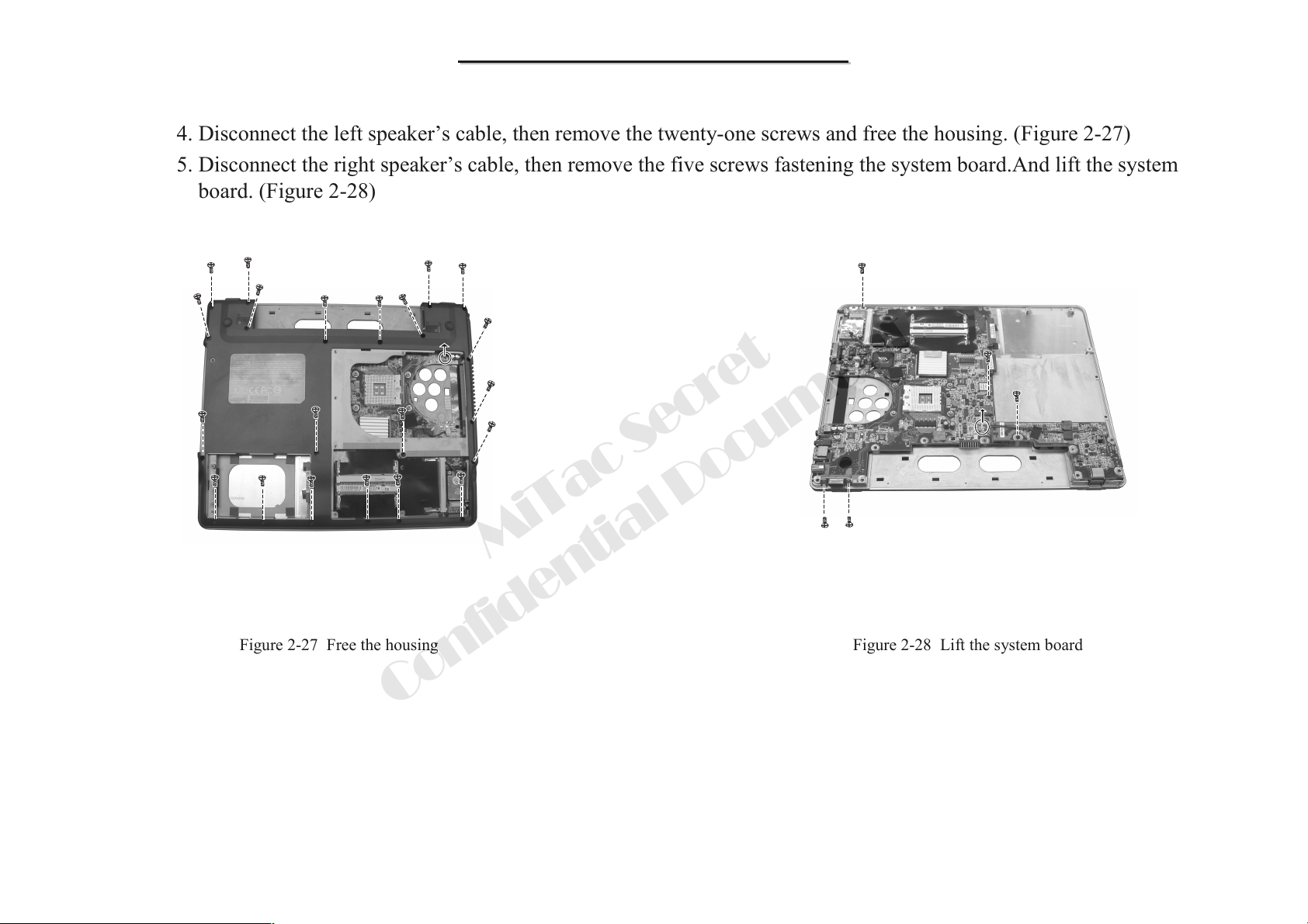
4. Disconnect the left speaker’s cable, then remove the twenty-one screws and free the housing. (Figure 2-27)
5. Disconnect the right speaker’s cable, then remove the five screws fastening the system board.And lift the system
board. (Figure 2-28)
Figure 2-27 Free the housing
Confidential Document
MiTac Secret
Figure 2-28 Lift the system board
73
Page 75
8666 N/B Maintenance
8666 N/B Maintenance
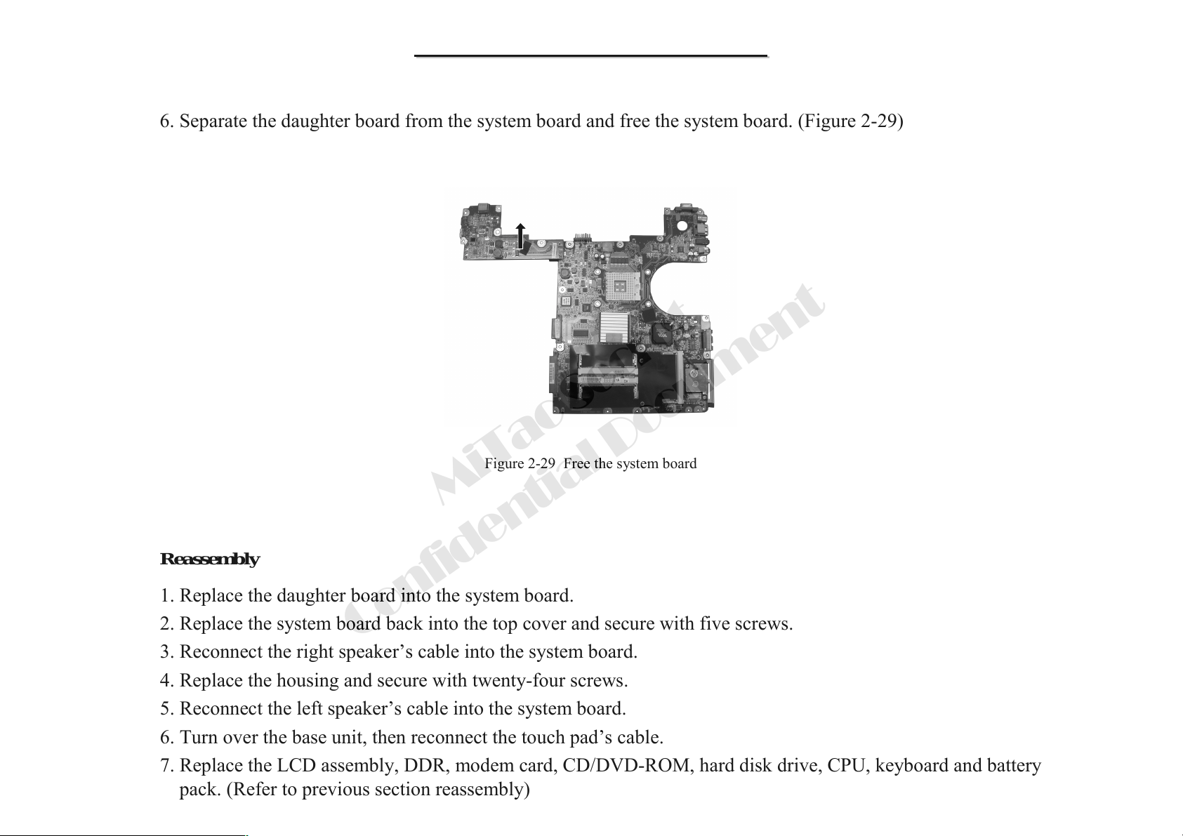
6. Separate the daughter board from the system board and free the system board. (Figure 2-29)
Figure 2-29 Free the system board
MiTac Secret
Reassembly
1. Replace the daughter board into the system board.
2. Replace the system board back into the top cover and secure with five screws.
3. Reconnect the right speaker’s cable into the system board.
4. Replace the housing and secure with twenty-four screws.
5. Reconnect the left speaker’s cable into the system board.
6. Turn over the base unit, then reconnect the touch pad’s cable.
7. Replace the LCD assembly, DDR, modem card, CD/DVD-ROM, hard disk drive, CPU, keyboard and battery
pack. (Refer to previous section reassembly)
Confidential Document
74
Page 76
8666 N/B Maintenance
8666 N/B Maintenance
2.3.12 Touch Pad
Disassembly
1. Remove the battery pack, keyboard, CPU, hard disk drive, CD/DVD-ROM drive, modem card, DDR, LCD
assembly and the system board. (See sections 2.3.1, 2.3.2, 2.3.3, 2.3.4, 2.3.5, 2.3.6, 2.3.7, 2.3.8 and 2.3.11
Disassembly)
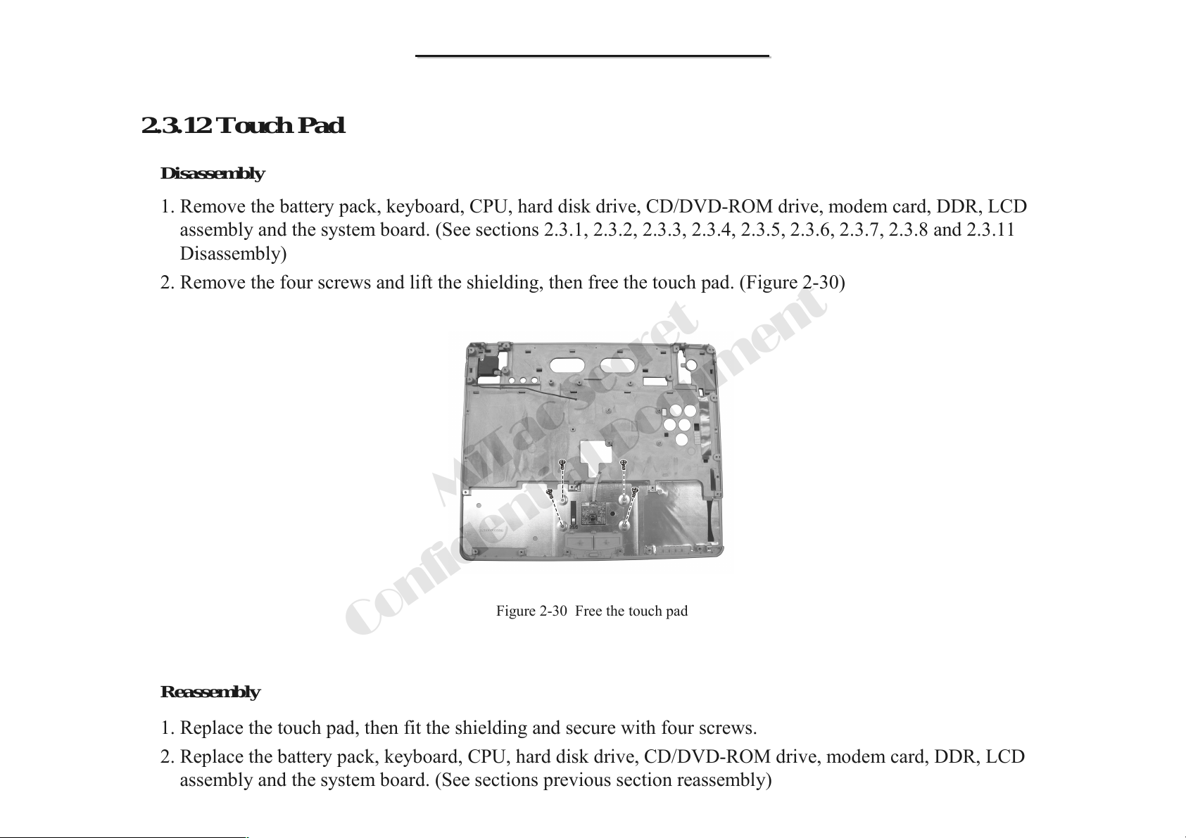
2. Remove the four screws and lift the shielding, then free the touch pad. (Figure 2-30)
MiTac Secret
Figure 2-30 Free the touch pad
Confidential Document
Reassembly
1. Replace the touch pad, then fit the shielding and secure with four screws.
2. Replace the battery pack, keyboard, CPU, hard disk drive, CD/DVD-ROM drive, modem card, DDR, LCD
assembly and the system board. (See sections previous section reassembly)
75
Page 77
8666 N/B Maintenance
8666 N/B Maintenance
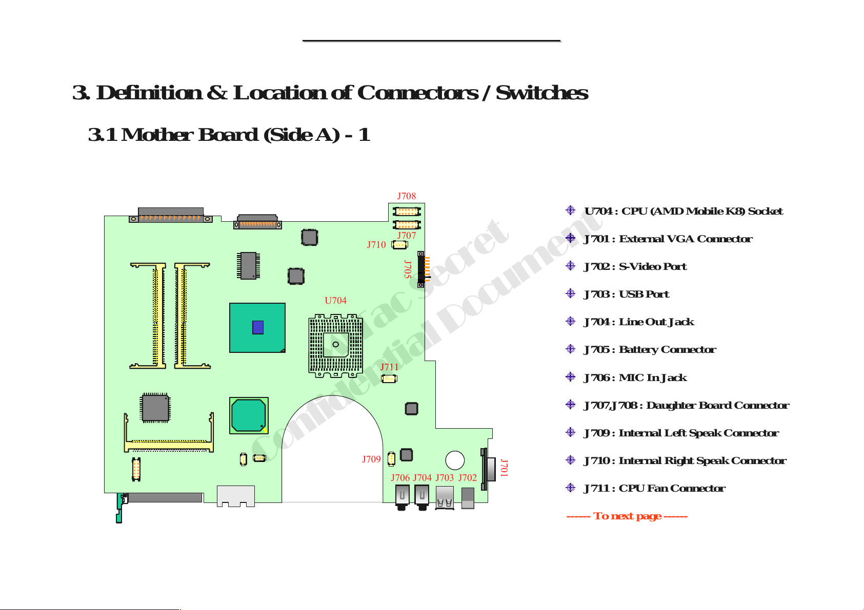
3. Definition & Location of Connectors / Switches
3.1 Mother Board (Side A) - 1
J708
U704 : CPU (AMD Mobile K8) Socket
J509
J707
J710
J705
U704
MiTac Secret
Confidential Document
J709
J711
J706
J701
J704 J703 J702
J701 : External VGA Connector
J702 : S-Video Port
J703 : USB Port
J704 : Line Out Jack
J705 : Battery Connector
J706 : MIC In Jack
J707,J708 : Daughter Board Connector
J709 : Internal Left Speak Connector
J710 : Internal Righ t Sp eak Conn ect or
J711 : CPU Fan Connector
------ To next page ------
76
Page 78
8666 N/B Maintenance
8666 N/B Maintenance
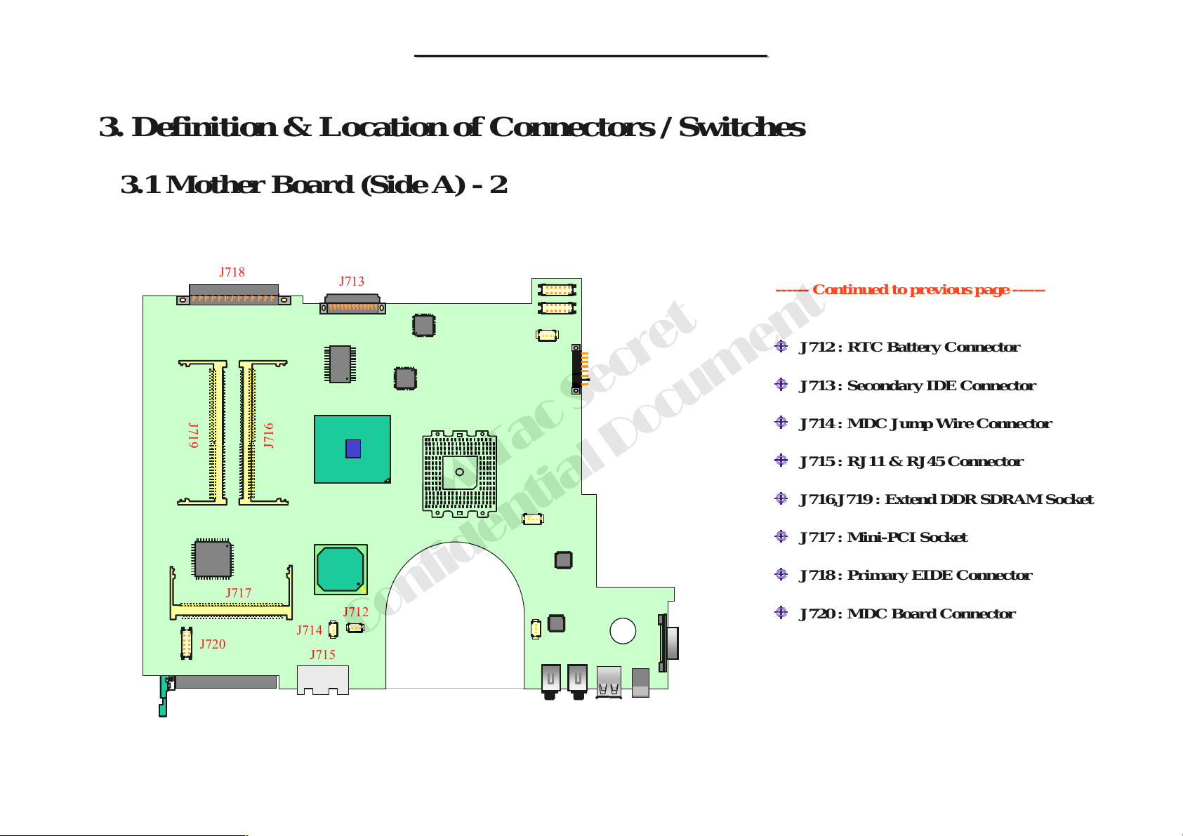
3. Definition & Location of Connectors / Switches
3.1 Mother Board (Side A) - 2
J719
J720
J718
J717
J509
J716
J714
J715
J713
MiTac Secret
J712
------ Continued to previous page ------
J712 : RTC Battery Conne ctor
J713 : Secondary IDE Connector
J714 : MDC Jump Wire Connector
J715 : RJ11 & RJ45 Connector
J716,J719 : Extend DDR SDRAM Socket
J717 : Mini-PCI Socket
J718 : Primary EIDE Connector
J720 : MDC Board Connector
Confidential Document
77
Page 79
8666 N/B Maintenance
8666 N/B Maintenance
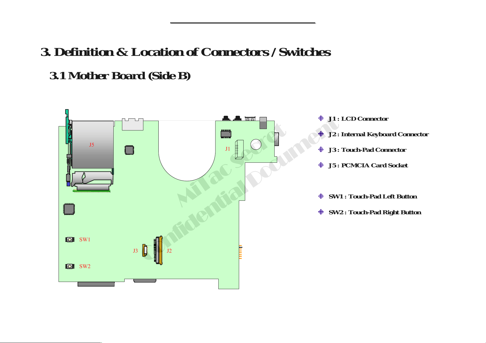
3. Definition & Location of Connectors / Switches
3.1 Mother Board (Side B)
J1 : LCD Connector
SW1
SW2
J5
J509
J2 : Internal Keyboard Connector
J1
J3 : Touch-Pad Connector
J5 : PCMCIA Card Socket
SW1 : Touch-Pad Left Button
MiTac Secret
SW2 : Touch-Pad Right Button
J2J3
Confidential Document
78
Page 80
8666 N/B Maintenance
8666 N/B Maintenance
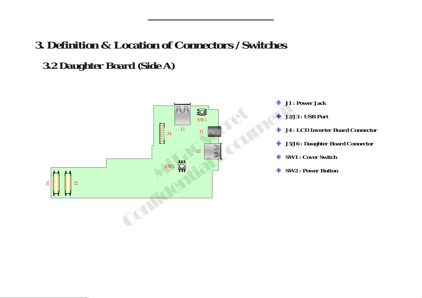
3. Definition & Location of Connectors / Switches
3.2 Daughter Board (Side A)
J1 : Power Jack
J6
J5
J2/J3 : USB Port
J4 : LCD Inverter Board Connector
J5/J6 : Daughter Board Connector
SW1 : Cover Switch
SW2 : Power Button
J4
SW2
J3
SW1
J1
J2
MiTac Secret
Confidential Document
79
Page 81
8666 N/B Maintenance
8666 N/B Maintenance
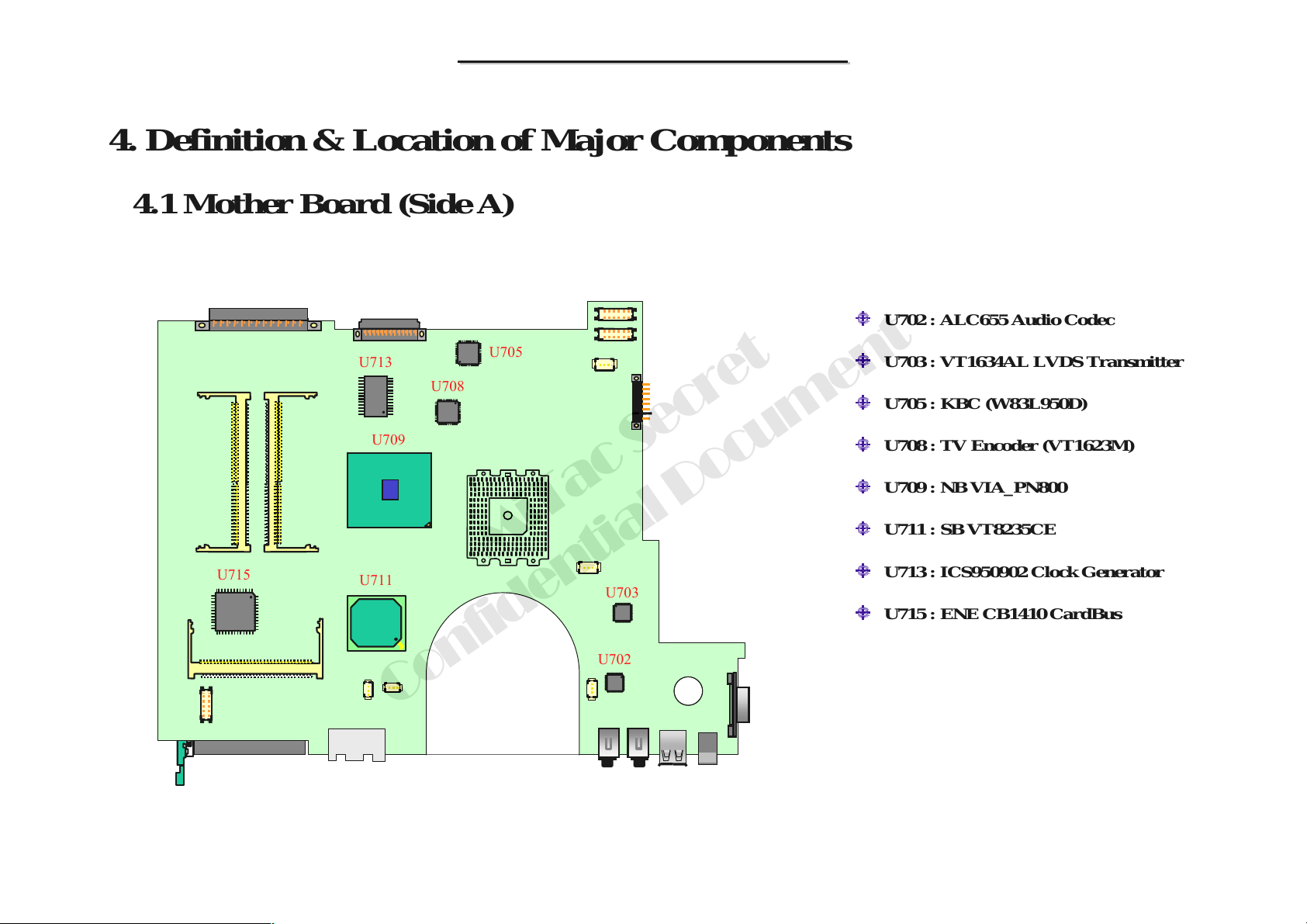
4. Definition & Location of Major Components
4.1 Mother Board (Side A)
U702 : ALC655 Audio Codec
U715
J509
U713
U708
U709
U705
U703 : VT1634AL LV DS Transmitter
U705 : KBC (W83L950D)
U708 : TV Encoder (VT1623M)
U709 : NB VIA_PN800
U711 : SB VT8235CE
MiTac Secret
U711
U703
U702
U713 : ICS950902 Clock Generator
U715 : ENE CB1410 CardBus
Confidential Document
80
Page 82
8666 N/B Maintenance
8666 N/B Maintenance
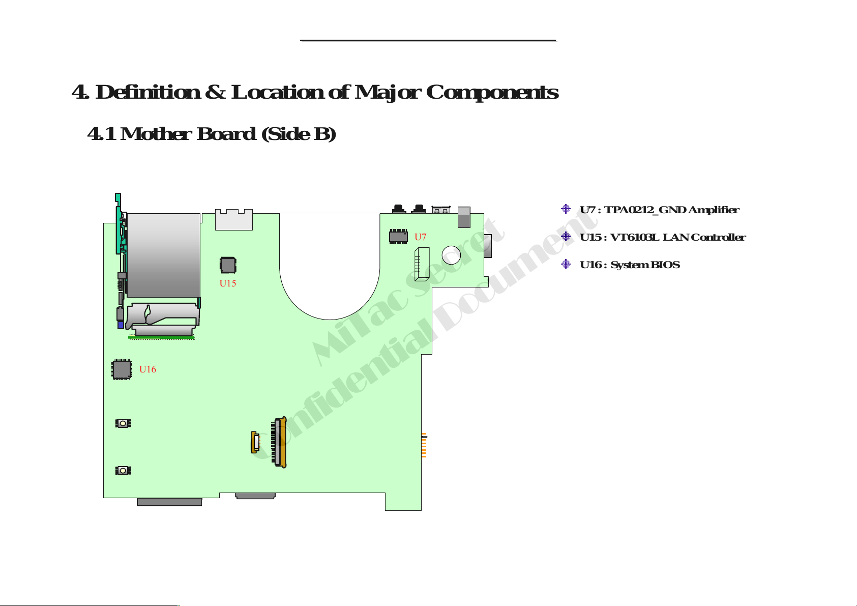
4. Definition & Location of Major Components
4.1 Mother Board (Side B)
U7 : TPA0212_GND Amplifier
U16
J509
U15
U7
U15 : VT6103L LAN Controller
U16 : System BIOS
MiTac Secret
Confidential Document
81
Page 83
8666 N/B Maintenance
p
b
8666 N/B Maintenance
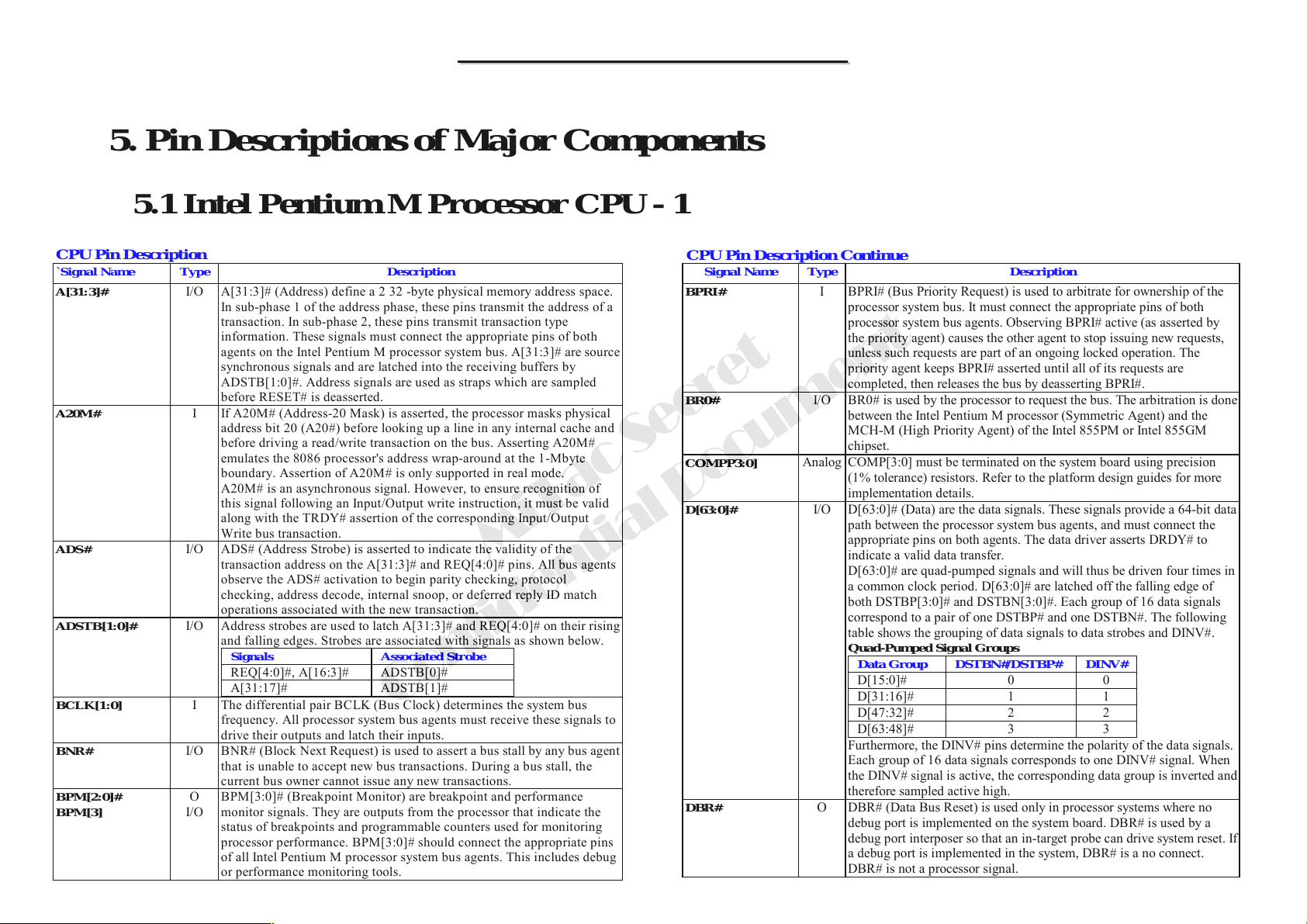
5. Pin Descriptions of Major Components
5.1 Intel Pentium M Processor CPU - 1
CPU Pin Description
`Signal Name Type Description
A[31:3]#
A20M#
ADS#
ADSTB[1:0]#
BCLK [1:0]
BNR#
BPM[2:0]#
BPM[3]
I/O A[31:3]# (Address) define a 2 32 -byte physical memory address space.
In sub-phase 1 of the address phase, these pins transmit the address of a
transaction. In sub-phase 2, these pins transmit transaction type
information. These signals must connect the appropriate pins of both
agents on the Intel Pentium M
synchronous signals and are latched into the receiving buffers by
ADSTB[1:0]#. Address signals are used as straps which are sampled
before RESET# is deasserted.
I If A20M# (Address-20 Mask) is asserted, the processor masks physical
address bit 20 (A20#) before looking up a line in any internal cache and
before driving a read/write transaction on the bus. Asserting A20M#
emulates the 8086 processor's address wrap-around at the 1-Mbyte
boundary. Assertion of A20M# is only supported in real mode.
A20M# is an asynchronous signal. However, to ensure recognition of
this signal following an Input/Output write instruction, it must be valid
along with the TRDY# assertion of the corresponding Input/Output
Write bus transaction.
I/O ADS# (Address Strobe) is asserted to indicate the validity of the
transaction address on the A[31:3]# and REQ[4:0]# pins. All bus agents
observe the ADS# activation to begin parity checking, protocol
checking, address decode, internal snoop, or deferred reply ID match
operations associated with the new transaction.
I/O Address strobes are used to latch A[31:3]# and REQ[4:0]# on their rising
and falling edges. Strobes are associated with signals as shown below.
Signals Associated Strobe
REQ[4:0]#, A[16:3]# ADSTB[0]#
A[31:17]# ADSTB[1]#
I The differential pair BCLK (Bus Clock) determines the system bus
frequency. All processor system bus agents must receive these signals to
drive their outputs and latch their inputs.
I/O BNR# (Block Next Request) is used to assert a bus stall by any bus agent
that is unable to accept new bus transactions. During a bus stall, the
current bus owner cannot issue any new transactions.
O
BPM[3:0]# (Breakpoint Monitor) are breakpoint and performance
I/O
monitor signals. They are outputs from the processor that indicate the
status of breakpoints and programmable counters used for monitoring
processor performance. BPM[3:0]# should connect the appropriate pins
of all Intel Pentium M processor system bus agents. This includes debug
or performance monitoring tools.
rocessor system bus. A[31:3]# are source
MiTac Secret
Confidential Document
CPU Pin Description Continue
Signal Name Type Description
BPRI#
BR0#
COMPP3:0]
D[63:0]#
DBR#
I BPRI# (Bus Priority Request) is used to arbitrate for ownership of the
processor system bus. It must connect the appropriate pins of both
processor system bus agents. Observing BPRI# active (as asserted by
the priority agent) causes the other agent to stop issuing new requests,
unless such requests are part of an ongoing locked operation. The
priority agent keeps BPRI# asserted until all of its requests are
completed, then releases the bus by deasserting BPRI#.
I/O BR0# is used by the processor to request the bus. The arbitration is done
between the Intel Pentium M processor (Symmetric Agent) and the
MCH-M (High Priority Agent) of the Intel 855PM or Intel 855GM
chipset.
Analog COMP[3:0] must be terminated on the system board using precision
(1% tolerance) resistors. Refer to the platform design guides for more
implementation details.
I/O D[63:0]# (Data) are the data signals. These signals provide a 64-
path between the processor system bus agents, and must connect the
appropriate pins on both agents. The data driver asserts DRDY# to
indicate a valid data transfer.
D[63:0]# are quad-pumped signals and will thus be driven four times in
a common clock period. D[63:0]# are latched off the falling edge of
both DSTBP[3:0]# and DSTBN[3:0]#. Each group of 16 data signals
correspond to a pair of one DSTBP# and one DSTBN#. The following
table shows the grouping of data signals to data strobes and DINV#.
Quad-Pumped Signal Groups
Data Group DSTBN#/DSTBP# DINV#
D[15:0]# 0 0
D[31:16]# 1 1
D[47:32]# 2 2
D[63:48]# 3 3
Furthermore, the DINV# pins determine the polarity of the data signals.
Each group of 16 data signals corresponds to one DINV# signal. When
the DINV# signal is active, the corresponding data group is inverted and
therefore sampled active high.
O DBR# (Data Bus Reset) is used only in processor systems where no
debug port is implemented on the system board. DBR# is used by a
debug port interposer so that an in-target probe can drive system reset. If
a debug port is implemented in the system, DBR# is a no connect.
DBR# is not a processor signal.
it data
82
Page 84
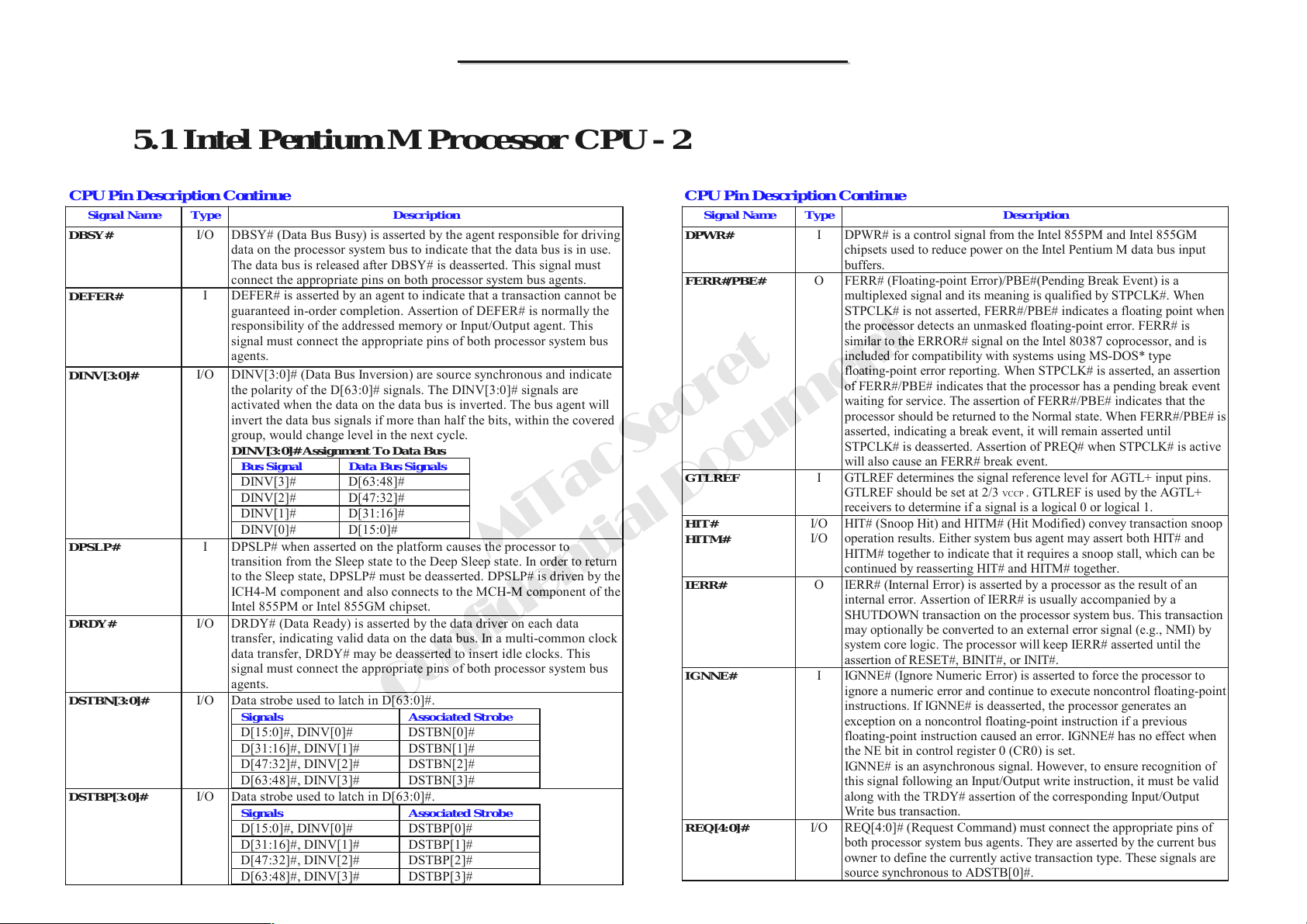
8666 N/B Maintenance
p
8666 N/B Maintenance
5.1 Intel Pentium M Processor CPU - 2
CPU Pin Description Continue CPU Pin Description Continue
Signal Name Type Description
DBSY#
DEFER#
DINV[3:0]#
DPSLP#
DRDY#
DSTBN[3:0]#
DSTBP[3:0]#
I/O DBSY# (Data Bus Busy) is asserted by the agent responsible for driving
data on the processor system bus to indicate that the data bus is in use.
The data bus is released after DBSY# is deasserted. This signal must
connect the appropriate pins on both processor system bus agents.
I DEFER# is asserted by an agent to indicate that a transaction cannot be
guaranteed in-order completion. Assertion of DEFER# is normally the
responsibility of the addressed memory or Input/Output agent. This
signal must connect the appropriate pins of both processor system bus
agents.
I/O DINV[3:0]# (Data Bus Inversion) are source synchronous and indicate
the polarity of the D[63:0]# signals. The DINV[3:0]# signals are
activated when the data on the data bus is inverted. The bus agent will
invert the data bus signals if more than half the bits, within the covered
group, would change level in the next cycle.
DINV[3:0]# Assignment To Data Bus
Bus Signal Data Bus Signals
DINV[3]# D[63:48]#
DINV[2]# D[47:32]#
DINV[1]# D[31:16]#
DINV[0]# D[15:0]#
I DPSLP# when asserted on the platform causes the processor to
transition from the Sleep state to the Deep Sleep state. In order to return
to the Sleep state, DPSLP# must be deasserted. DPSLP# is driven by the
ICH4-M component and also connects to the MCH-M component of the
Intel 855PM or Intel 855GM chipset.
I/O DRDY# (Data Ready) is asserted by the data driver on each data
transfer, indicating valid data on the data bus. In a multi-common clock
data transfer, DRDY# may be deasserted to insert idle clocks. This
signal must connect the appropriate pins of both processor system bus
agents.
I/O Data strobe used to latch in D[63:0]#.
Signals Associated Strobe
D[15:0]#, DINV[0]# DSTBN[0]#
D[31:16]#, DINV[1]# DSTBN[1]#
D[47:32]#, DINV[2]# DSTBN[2]#
D[63:48]#, DINV[3]# DSTBN[3]#
I/O Data strobe used to latch in D[63:0]#.
Signals Associated Strobe
D[15:0]#, DINV[0]# DSTBP[0]#
D[31:16]#, DINV[1]# DSTBP[1]#
D[47:32]#, DINV[2]# DSTBP[2]#
D[63:48]#, DINV[3]# DSTBP[3]#
Confidential Document
MiTac Secret
Signal Name Type Description
DPWR#
FERR#/PBE#
GTLREF
HIT#
HITM#
IERR#
IGNNE#
REQ[4:0]#
I DPWR# is a control signal from the Intel 855PM and Intel 855GM
chipsets used to reduce power on the Intel Pentium M data bus input
buffers.
O FERR# (Floating-point Error)/PBE#(Pending Break Event) is a
multiplexed signal and its meaning is qualified by STPCLK#. When
STPCLK# is not asserted, FERR#/PBE# indicates a floating point when
the processor detects an unmasked floating-point error. FERR# is
similar to the ERROR# signal on the Intel 80387 coprocessor, and is
included for compatibility with systems using MS-DOS* type
floating-point error reporting. When STPCLK# is asserted, an assertion
of FERR#/PBE# indicates that the processor has a pending break event
waiting for service. The assertion of FERR#/PBE# indicates that the
processor should be returned to the Normal state. When FERR#/PBE# is
asserted, indicating a break event, it will remain asserted until
STPCLK# is deasserted. Assertion of PREQ# when STPCLK# is active
will also cause an FERR# break event.
I GTLREF determines the signal reference level for AGTL+ input pins.
GTLREF should be set at 2/3
receivers to determine if a signal is a logical 0 or logical 1.
I/O
HIT# (Snoop Hit) and HITM# (Hit Modified) convey transaction snoop
I/O
operation results. Either system bus agent may assert both HIT# and
HITM# together to indicate that it requires a snoop stall, which can be
continued by reasserting HIT# and HITM# together.
O IERR# (Internal Error) is asserted by a processor as the result of an
internal error. Assertion of IERR# is usually accompanied by a
SHUTDOWN transaction on the processor system bus. This transaction
may optionally be converted to an external error signal (e.g., NMI) by
system core logic. The processor will keep IERR# asserted until the
assertion of RESET#, BINIT#, or INIT#.
I IGNNE# (Ignore Numeric Error) is asserted to force the processor to
ignore a numeric error and continue to execute noncontrol floating-
instructions. If IGNNE# is deasserted, the processor generates an
exception on a noncontrol floating-point instruction if a previous
floating-point instruction caused an error. IGNNE# has no effect when
the NE bit in control register 0 (CR0) is set.
IGNNE# is an asynchronous signal. However, to ensure recognition of
this signal following an Input/Output write instruction, it must be valid
along with the TRDY# assertion of the corresponding Input/Output
Write bus transaction.
I/O REQ[4:0]# (Request Command) must connect the appropriate pins of
both processor system bus agents. They are asserted by the current bus
owner to define the currently active transaction type. These signals are
source synchronous to ADSTB[0]#.
VCCP . GTLREF is used by the AGTL+
oint
83
Page 85
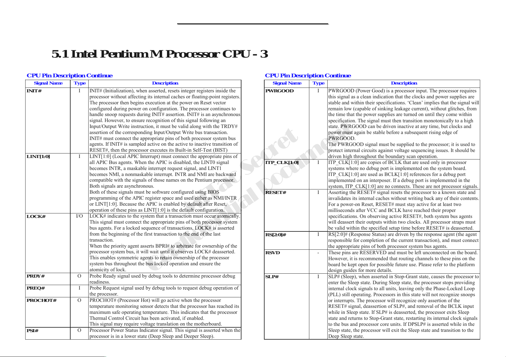
8666 N/B Maintenance
p
8666 N/B Maintenance
5.1 Intel Pentium M Processor CPU - 3
CPU Pin Description Continue
Signal Name Type Description
INIT#
LINT[1:0]
LOCK#
PRDY#
PREQ#
PROCHOT#
PSI#
I INIT# (Initialization), when asserted, resets integer registers inside the
processor without affecting its internal caches or floating-
The processor then begins execution at the power on Reset vector
configured during power on configuration. The processor continues to
handle snoop requests during INIT# assertion. INIT# is an asynchronous
signal. However, to ensure recognition of this signal following an
Input/Output Write instruction, it must be valid along with the TRDY#
assertion of the corresponding Input/Output Write bus transaction.
INIT# must connect the appropriate pins of both processor system bus
agents. If INIT# is sampled active on the active to inactive transition of
RESET#, then the processor executes its Built-in Self-Test (BIST)
I LINT[1:0] (Local APIC Interrupt) must connect the appropriate pins of
all APIC Bus agents. When the APIC is disabled, the LINT0 signal
becomes INTR, a maskable interrupt request signal, and LINT1
becomes NMI, a nonmaskable interrupt. INTR and NMI are backward
compatible with the signals of those names on the Pentium processor.
Both signals are asynchronous.
Both of these signals must be software configured using BIOS
programming of the APIC register space and used either as NMI/INTR
or LINT[1:0]. Because the APIC is enabled by default after Reset,
operation of these pins as LINT[1:0] is the default configuration.
I/O LOCK# indicates to the system that a transaction must occur atomically.
This signal must connect the appropriate pins of both processor system
bus agents. For a locked sequence of transactions, LOCK# is asserted
from the beginning of the first transaction to the end of the last
transaction.
When the priority agent asserts BPRI# to arbitrate for ownership of the
processor system bus, it will wait until it observes LOCK# deasserted.
This enables symmetric agents to retain ownership of the processor
system bus throughout the bus locked operation and ensure the
atomicity of lock.
O Probe Ready signal used by debug tools to determine processor debug
readiness.
I Probe Request signal used by debug tools to request debug operation of
the processor.
O PROCHOT# (Processor Hot) will go active when the processor
temperature monitoring sensor detects that the processor has reached its
maximum safe operating temperature. This indicates that the processor
Thermal Control Circuit has been activated, if enabled.
This signal may require voltage translation on the motherboard.
O Processor Power Status Indicator signal. This signal is asserted when the
processor is in a lower state (Deep Sleep and Deeper Sleep).
Confidential Document
MiTac Secret
oint registers.
CPU Pin Description Continue
Signal Name Type Description
PWRGOOD
ITP_CLK[1:0]
RESET#
RS[2:0]#
RSVD
SLP#
I PWRGOOD (Power Good) is a processor input. The processor requires
this signal as a clean indication that the clocks and power supplies are
stable and within their specifications. ‘Clean’ implies that the signal will
remain low (capable of sinking leakage current), without glitches, from
the time that the power supplies are turned on until they come within
specification. The signal must then transition monotonically to a high
state. PWRGOOD can be driven inactive at any time, but clocks and
power must again be stable before a subsequent rising edge of
PWRGOOD.
The PWRGOOD signal must be supplied to the processor; it is used to
protect internal circuits against voltage sequencing issues. It should be
driven high throughout the boundary scan operation.
I ITP_CLK[1:0] are copies of BCLK that are used only in processor
systems where no debug port is implemented on the system board.
ITP_CLK[1:0] are used as BCLK[1:0] references for a debug port
implemented on an interposer. If a debug port is implemented in the
system, ITP_CLK[1:0] are no connects. These are not processor signals.
I Asserting the RESET# signal resets the processor to a known state and
invalidates its internal caches without writing back any of their contents.
For a power-on Reset, RESET# must stay active for at least two
milliseconds after VCC and BCLK have reached their proper
specifications. On observing active RESET#, both system bus agents
will deassert their outputs within two clocks. All processor straps must
be valid within the specified setup time before RESET# is deasserted.
I RS[2:0]# (Response Status) are driven by the response agent (the agent
responsible for completion of the current transaction), and must connect
the appropriate pins of both processor system bus agents.
- These pins are RESERVED and must be left unconnected on the board.
However, it is recommended that routing channels to these pins on the
board be kept open for possible future use. Please refer to the platform
design guides for more details.
I SLP# (Sleep), when asserted in Stop-Grant state, causes the processor to
enter the Sleep state. During Sleep state, the processor stops providing
internal clock signals to all units, leaving only the Phase-Locked Loop
(PLL) still operating. Processors in this state will not recognize snoops
or interrupts. The processor will recognize only assertion of the
RESET# signal, deassertion of SLP#, and removal of the BCLK input
while in Sleep state. If SLP# is deasserted, the processor exits Sleep
state and returns to Stop-Grant state, restarting its internal clock signals
to the bus and processor core units. If DPSLP# is asserted while in the
Sleep state, the processor will exit the Sleep state and transition to the
Deep Sleep state.
84
Page 86
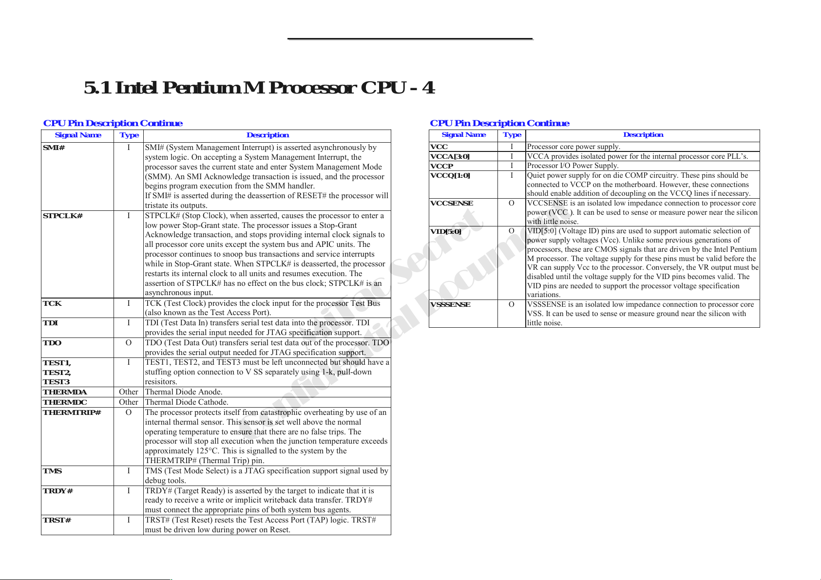
8666 N/B Maintenance
8666 N/B Maintenance
5.1 Intel Pentium M Processor CPU - 4
CPU Pin Description Continue
Signal Name Type Description
SMI#
STPCLK#
TCK
TDI
TDO
TEST1,
TEST2,
TEST3
THERMDA
THERMDC
THERMTRIP#
TMS
TRDY#
TRST#
I SMI# (System Management Interrupt) is asserted asynchronously by
system logic. On accepting a System Management Interrupt, the
processor saves the current state and enter System Management Mode
(SMM). An SMI Acknowledge transaction is issued, and the processor
begins program execution from the SMM handler.
If SMI# is asserted during the deassertion of RESET# the processor will
tristate its outputs.
I STPCLK# (Stop Clock), when asserted, causes the processor to enter a
low power Stop-Grant state. The processor issues a Stop-Grant
Acknowledge transaction, and stops providing internal clock signals to
all processor core units except the system bus and APIC units. The
processor continues to snoop bus transactions and service interrupts
while in Stop-Grant state. When STPCLK# is deasserted, the processor
restarts its internal clock to all units and resumes execution. The
assertion of STPCLK# has no effect on the bus clock; STPCLK# is an
asynchronous input.
I TCK (Test Clock) provides the clock input for the processor Test Bus
(also known as the Test Access Port).
I TDI (Test Data In) transfers serial test data into the processor. TDI
provides the serial input needed for JTAG specification support.
O TDO (Test Data Out) transfers serial test data out of the processor. TDO
provides the serial output needed for JTAG specification support.
I TEST1, TEST2, and TEST3 must be left unconnected but should have a
stuffing option connection to V SS separately using 1-k, pull-down
resisitors.
Other Thermal Diode Anode.
Other Thermal Diode Cathode.
O The processor protects itself from catastrophic overheating by use of an
internal thermal sensor. This sensor is set well above the normal
operating temperature to ensure that there are no false trips. The
processor will stop all execution when the junction temperature exceeds
approximately 125°C. This is signalled to the system by the
THERMTRIP# (Thermal Trip) pin.
I TMS (Test Mode Select) is a JTAG specification support signal used by
debug tools.
I TRDY# (Target Ready) is asserted by the target to indicate that it is
ready to receive a write or implicit writeback data transfer. TRDY#
must connect the appropriate pins of both system bus agents.
I TRST# (Test Reset) resets the Test Access Port (TAP) logic. TRST#
must be driven low during power on Reset.
Confidential Document
CPU Pin Description Continue
Signal Name Type Description
VCC
VCCA[3:0]
VCCP
VCCQ[1:0]
VCCSENSE
VID[5:0]
VSSSENSE
I Processor core power supply.
I VCCA provides isolated power for the internal processor core PLL’s.
I Processor I/O Power Supply.
I Quiet power supply for on die COMP circuitry. These pins should be
O VCCSENSE is an isolated low impedance connection to processor core
O VID[5:0] (Voltage ID) pins are used to support automatic selection of
O VSSSENSE is an isolated low impedance connection to processor core
MiTac Secret
connected to VCCP on the motherboard. However, these connections
should enable addition of decoupling on the VCCQ lines if necessary.
power (VCC ). It can be used to sense or measure power near the silicon
with little noise.
power supply voltages (Vcc). Unlike some previous generations of
processors, these are CMOS signals that are driven by the Intel Pentium
M processor. The voltage supply for these pins must be valid before the
VR can supply Vcc to the processor. Conversely, the VR output must be
disabled until the voltage supply for the VID pins becomes valid. The
VID pins are needed to support the processor voltage specification
variations.
VSS. It can be used to sense or measure ground near the silicon with
little noise.
85
Page 87
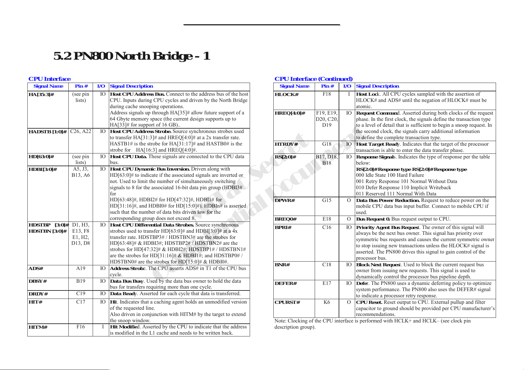
8666 N/B Maintenance
8666 N/B Maintenance
5.2 PN800 North Bridge - 1
CPU Interface
Signal Name Pin # I/O Signal Description
HA[35:3]#
HADSTB [1:0]#
HD[63:0]#
HDBI[3:0]#
HDSTBP [3:0]#
HDSTBN [3:0]#
ADS#
DBSY#
DRDY#
HIT#
HITM#
(see pin
lists)
C26, A22 IO Host CPU Address Strobe. Source synchronous strobes used
(see pin
lists)
A5, J3,
B13, A6
D1, H3,
E13, F8
E1, H2,
D13, D8
A19 IO Address Strobe. The CPU asserts ADS# in T1 of the CPU bus
B19 IO
C19 IO Data Ready. Asserted for each cycle that data is transferred.
C17 IO Hit. Indicates that a caching agent holds an unmodified version
F16 I Hit Modified. Asserted by the CPU to indicate that the address
IO Host CPU Address Bus. Connect to the address bus of the host
CPU. Inputs during CPU cycles and driven by the North Bridge
during cache snooping operations.
Address signals up through HA[35]# allow future support of a
64 Gbyte memory space (the current design supports up to
HA[33]# for support of 16 GB)..
to transfer HA[31:3]# and HREQ[4:0]# at a 2x transfer rate.
HASTB1# is the strobe for HA[31:17]# and HASTB0# is the
strobe for HA[16:3] and HREQ[4:0]#.
IO Host CPU Data. These signals are connected to the CPU data
bus.
IO Host CPU Dynamic Bus Inversion. Driven along with
HD[63:0]# to indicate if the associated signals are inverted or
not. Used to limit the number of simultaneously switching
signals to 8 for the associated 16-bit data pin group (HDBI3#
for
HD[63:48]#, HDBI2# for HD[47:32]#, HDBI1# for
HD[31:16]#, and HDBI0# for HD[15:0]#). HDBIn# is asserted
such that the number of data bits driven low for the
corresponding group does not exceed 8.
IO Host CPU Differential Data Strobes. Source synchronous
strobes used to transfer HD[63:0]# and HDBI[3:0]# at a 4x
transfer rate. HDSTBP3# / HDSTBN3# are the strobes for
HD[63:48]# & HDBI3#; HDSTBP2# / HDSTBN2# are the
strobes for HD[47:32]# & HDBI2#; HDSTBP1# / HDSTBN1#
are the strobes for HD[31:16]# & HDBI1#; and HDSTBP0# /
HDSTBN0# are the strobes for HD[15:0]# & HDBI0#.
cycle.
Data Bus Bus
bus for transfers requiring more than one cycle.
of the requested line.
Also driven in conjunction with HITM# by the target to extend
the snoop window.
is modified in the L1 cache and needs to be written back.
CPU Interface (Continued)
Signal Name Pin # I/O Signal Description
HLOCK#
HREQ[4:0]#
HTRDY#
RS[2:0]#
DPWR#
MiTac Secret
y. Used by the data bus owner to hold the data
Confidential Document
BREQ0#
BPRI#
BNR#
DEFER#
CPURST#
Note: Clocking of the CPU interface is performed with HCLK+ and HCLK– (see clock pin
description group).
F18 I Host Lock. All CPU cycles sampled with the assertion of
F19, E19,
D20, C20,
D19
G18 IO Host Target Ready. Indicates that the target of the processor
B17, D18,
B18
G15 O Data Bus Power Reduction. Request to reduce power on the
E18 O Bus Request 0. Bus request output to CPU.
C16 IO Priority Agent Bus Request. The owner of this signal will
C18 IO Block Next Request. Used to block the current request bus
E17 IO Defer. The PN800 uses a dynamic deferring policy to optimize
K6 O CPU Reset. Reset output to CPU. External pullup and filter
HLOCK# and ADS# until the negation of HLOCK# must be
atomic.
IO Request Command. Asserted during both clocks of the request
phase. In the first clock, the signals define the transaction type
to a level of detail that is sufficient to begin a snoop request. In
the second clock, the signals carry additional information
to define the complete transaction type.
transaction is able to enter the data transfer phase.
IO Response Signals. Indicates the type of response per the table
below:
RS[2:0]# Response type RS[2:0]# Response type
000 Idle State 100 Hard Failure
001 Retry Response 101 Normal Without Data
010 Defer Response 110 Implicit Writeback
011 Reserved 111 Normal With Data
mobile CPU data bus input buffer. Connect to mobile CPU if
used.
always be the next bus owner. This signal has priority over
symmetric bus requests and causes the current symmetric owner
to stop issuing new transactions unless the HLOCK# signal is
asserted. The PN800 drives this signal to gain control of the
processor bus.
owner from issuing new requests. This signal is used to
dynamically control the processor bus pipeline depth.
system performance. The PN800 also uses the DEFER# signal
to indicate a processor retry response.
capacitor to ground should be provided per CPU manufacturer’s
recommendations.
86
Page 88
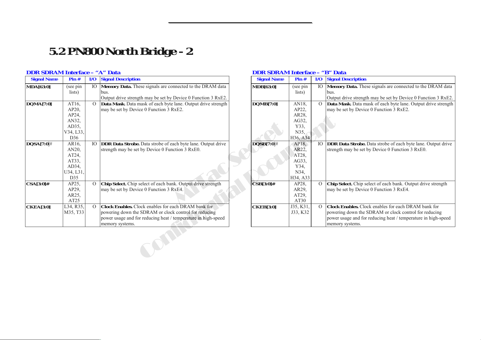
8666 N/B Maintenance
8666 N/B Maintenance
5.2 PN800 North Bridge - 2
DDR SDRAM Interface – “A” Data
Signal Name Pin # I/O Signal Description
MDA[63:0]
DQMA[7:0]
DQSA[7:0]# AR16,
CSA[3:0]#
CKEA[3:0]
(see pin
lists)
AT16,
AP20,
AP24,
AN32,
AD35,
V34, L33,
D36
AN20,
AT24,
AT33,
AD34,
U34, L31,
D35
AP25,
AP29,
AR25,
AT25
L34, R35,
M35, T33
IO Memory Data. These signals are connected to the DRAM data
bus.
Output drive strength may be set by Device 0 Function 3 RxE2.
O Data Mask. Data mask of each byte lane. Output drive strength
may be set by Device 0 Function 3 RxE2.
IO DDR Data Strobe. Data strobe of each byte lane. Output drive
strength may be set by Device 0 Function 3 RxE0.
O Chip Select. Chip select of each bank. Output drive strength
may be set by Device 0 Function 3 RxE4.
O Clock Enables. Clock enables for each DRAM bank for
powering down the SDRAM or clock control for reducing
power usage and for reducing heat / temperature in high-speed
memory systems.
DDR SDRAM Interface – “B” Data
Signal Name Pin # I/O Signal Description
MDB[63:0]
DQMB[7:0]
DQSB[7:0]# AP18,
CSB[3:0]#
MiTac Secret
CKEB[3:0]
(see pin
lists)
AN18,
AP22,
AR28,
AG32,
Y33,
N35,
H36, A34
AR22,
AT28,
AG33,
Y34,
N34,
H34, A33
AP28,
AR29,
AT29,
AT30
J35, K31,
J33, K32
IO Memory Data. These signals are connected to the DRAM data
bus.
Output drive strength may be set by Device 0 Function 3 RxE2.
O Data Mask. Data mask of each byte lane. Output drive strength
may be set by Device 0 Function 3 RxE2.
IO DDR Data Strobe. Data strobe of each byte lane. Output drive
strength may be set by Device 0 Function 3 RxE0.
O Chip Select. Chip select of each bank. Output drive strength
may be set by Device 0 Function 3 RxE4.
O Clock Enables. Clock enables for each DRAM bank for
powering down the SDRAM or clock control for reducing
power usage and for reducing heat / temperature in high-speed
memory systems.
Confidential Document
87
Page 89
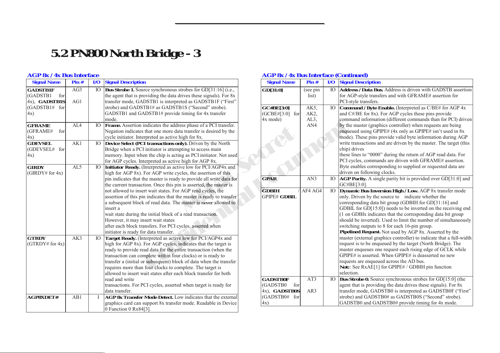
8666 N/B Maintenance
8666 N/B Maintenance
5.2 PN800 North Bridge - 3
AGP 8x / 4x Bus Interface
Signal Name Pin # I/O Signal Description
GADSTB1F
(GADSTB1 for
4x), GADSTB1S
(GADSTB1# for
4x)
GFRAME
(GFRAME# for
4x)
GDEVSEL
(GDEVSEL# for
4x)
GIRDY
(GIRDY# for 4x)
GTRDY
(GTRDY# for 4x)
AGP8XDET#
AG3
AG1
AL4 IO Frame. Assertion indicates the address phase of a PCI transfer.
AK1 IO Device Select (PCI transactions only). Driven by the North
AL5 IO Initiator Ready. (Interpreted as active low for PCI/AGP4x and
AK3 IO Target Ready. (Interpreted as active low for PCI/AGP4x and
AB1 I AGP 8x Tr an s fe r M od e D e t ect. Low indicates that the external
IO Bus Strobe 1. Source synchronous strobes for GD[31:16] (i.e.,
the agent that is providing the data drives these signals). For 8x
transfer mode, GADSTB1 is interpreted as GADSTB1F (“First”
strobe) and GADSTB1# as GADSTB1S (“Second” strobe).
GADSTB1 and GADSTB1# provide timing for 4x transfer
mode.
Negation indicates that one more data transfer is desired by the
cycle initiator. Interpreted as active high for 8x.
Bridge when a PCI initiator is attempting to access main
memory. Input when the chip is acting as PCI initiator. Not used
for AGP cycles. Interpreted as active high for AGP 8x.
high for AGP 8x). For AGP write cycles, the assertion of this
pin indicates that the master is ready to provide all write data for
the current transaction. Once this pin is asserted, the master is
not allowed to insert wait states. For AGP read cycles, the
assertion of this pin indicates that the master is ready to transfer
a subsequent block of read data. The master is never allowed to
insert a
wait state during the initial block of a read transaction.
However, it may insert wait states
after each block transfers. For PCI cycles, asserted when
initiator is ready for data transfer.
high for AGP 8x). For AGP cycles, indicates that the target is
ready to provide read data for the entire transaction (when the
transaction can complete within four clocks) or is ready to
transfer a (initial or subsequent) block of data when the transfer
requires more than four clocks to complete. The target is
allowed to insert wait states after each block transfer for both
read and write
transactions. For PCI cycles, asserted when target is ready for
data transfer.
graphics card can support 8x transfer mode. Readable in Device
0 Function 0 Rx84[3].
AGP 8x / 4x Bus Interface (Continued)
Signal Name Pin # I/O Signal Description
GD[31:0]
GC#BE[3:0]
(GCBE#[3:0] for
4x mode)
GPAR
GDBIH /
GPIPE# GDBIL
(see pin
list)
AK5,
AK2,
AL3,
AN4
AN3 IO AGP Parity. A single parity bit is provided over GD[31:0] and
AF4 AG4 IO Dynamic Bus Inversion High / Low. AGP 8x transfer mode
MiTac Secret
Confidential Document
GADSTB0F
(GADSTB0 for
4x), GADSTB0S
(GADSTB0# for
4x)
AT3
AR3
IO Address / Data Bus. Address is driven with GADSTB assertion
for AGP-style transfers and with GFRAME# assertion for
PCI-style transfers.
IO Command / Byte Enable. (Interpreted as C/BE# for AGP 4x
and C#/BE for 8x). For AGP cycles these pins provide
command information (different commands than for PCI) driven
by the master (graphics controller) when requests are being
enqueued using GPIPE# (4x only as GPIPE# isn’t used in 8x
mode). These pins provide valid byte information during AGP
write transactions and are driven by the master. The target (this
chip) drives
these lines to “0000” during the return of AGP read data. For
PCI cycles, commands are driven with GFRAME# assertion.
Byte enables corresponding to supplied or requested data are
driven on following clocks.
GC#BE[3:0].
only. Driven by the source to indicate whether the
corresponding data bit group (GDBIH for GD[31:16] and
GDBIL for GD[15:0]) needs to be inverted on the receiving end
(1 on GDBIx indicates that the corresponding data bit group
should be inverted). Used to limit the number of simultaneously
switching outputs to 8 for each 16-pin group.
Pipelined Request.
master (external graphics controller) to indicate that a full-width
request is to be enqueued by the target (North Bridge). The
master enqueues one request each rising edge of GCLK while
GPIPE# is asserted. When GPIPE# is deasserted no new
requests are enqueued across the AD bus.
Note: See RxAE[1] for GPIPE# / GDBIH pin function
selection.
IO Bus Strobe 0. Source synchronous strobes for GD[15:0] (the
agent that is providing the data drives these signals). For 8x
transfer mode, GADSTB0 is interpreted as GADSTB0F (“First”
strobe) and GADSTB0# as GADSTB0S (“Second” strobe).
GADSTB0 and GADSTB0# provide timing for 4x mode.
Not used by AGP 8x. Asserted by the
88
Page 90
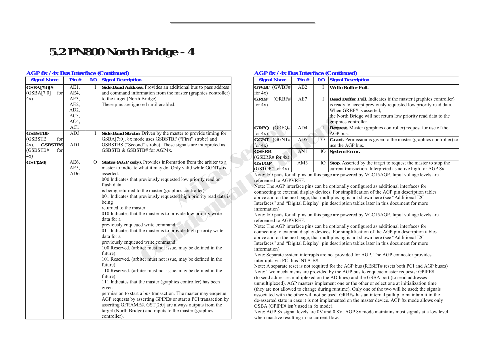
8666 N/B Maintenance
8666 N/B Maintenance
5.2 PN800 North Bridge - 4
AGP 8x / 4x Bus Interface (Continued)
Signal Name Pin # I/O Signal Description
GSBA[7:0]#
(GSBA[7:0] for
4x)
GSBSTBF
(GSBSTB for
4x), GSBSTBS
(GSBSTB# for
4x)
GST[2:0]
AE1,
AE4,
AE3,
AE2,
AD2,
AC3,
AC4,
AC1
AD3
AD1
AE6,
AE5,
AD6
I Side Band Address. Provides an additional bus to pass address
and command information from the master (graphics controller)
to the target (North Bridge).
These pins are ignored until enabled.
Side Band Strobe.
I
GSBA[7:0]. 8x mode uses GSBSTBF (“First” strobe) and
GSBSTBS (“Second” strobe). These signals are interpreted as
GSBSTB & GSBSTB# for AGP4x.
O Status (AGP only). Provides information from the arbiter to a
master to indicate what it may do. Only valid while GGNT# is
asserted.
000 Indicates that previously requested low priority read or
flush data
is being returned to the master (graphics controller).
001 Indicates that previously requested high priority read data is
being
returned to the master.
010 Indicates that the master is to provide low priority write
data for a
previously enqueued write command.
011 Indicates that the master is to provide high priority write
data for a
previously enqueued write command.
100 Reserved. (arbiter must not issue, may be defined in the
future).
101 Reserved. (arbiter must not issue, may be defined in the
future).
110 Reserved. (arbiter must not issue, may be defined in the
future).
111 Indicates that the master (graphics controller) has been
given
permission to start a bus transaction. The master may enqueue
AGP requests by asserting GPIPE# or start a PCI transaction by
asserting GFRAME#. GST[2:0] are always outputs from the
target (North Bridge) and inputs to the master (graphics
controller).
AGP 8x / 4x Bus Interface (Continued)
Signal Name Pin # I/O Signal Description
GWBF (GWBF#
for 4x)
Driven by the master to provide timing for
MiTac Secret
Confidential Document
GRBF (GRBF#
for 4x)
GREQ (GREQ#
for 4x)
GGNT (GGNT#
for 4x)
GSERR
(GSERR# for 4x)
GSTOP
(GSTOP# for 4x)
Note: I/O pads for all pins on this page are powered by VCC15AGP. Input voltage levels are
referenced to AGPVREF.
Note: The AGP interface pins can be optionally configured as additional interfaces for
connecting to external display devices. For simplification of the AGP pin description tables
above and on the next page, that multiplexing is not shown here (see “Additional I2C
Interfaces” and “Digital Display” pin description tables later in this document for more
information).
Note: I/O pads for all pins on this page are powered by VCC15AGP. Input voltage levels are
referenced to AGPVREF.
Note: The AGP interface pins can be optionally configured as additional interfaces for
connecting to external display devices. For simplification of the AGP pin description tables
above and on the next page, that multiplexing is not shown here (see “Additional I2C
Interfaces” and “Digital Display” pin description tables later in this document for more
information).
Note: Separate system interrupts are not provided for AGP. The AGP connector provides
interrupts via PCI bus INTA-B#.
Note: A separate reset is not required for the AGP bus (RESET# resets both PCI and AGP buses)
Note: Two mechanisms are provided by the AGP bus to enqueue master requests: GPIPE#
(to send addresses multiplexed on the AD lines) and the GSBA port (to send addresses
unmultiplexed). AGP masters implement one or the other or select one at initialization time
(they are not allowed to change during runtime). Only one of the two will be used; the signals
associated with the other will not be used. GRBF# has an internal pullup to maintain it in the
de-asserted state in case it is not implemented on the master device. AGP 8x mode allows only
GSBA (GPIPE# isn’t used in 8x mode).
Note: AGP 8x signal levels are 0V and 0.8V. AGP 8x mode maintains most signals at a low level
when inactive resulting in no current flow.
AB2 I
AE7 I Read Buffer Full. Indicates if the master (graphics controller)
AD4 I Request. Master (graphics controller) request for use of the
AD5 O Grant. Permission is given to the master (graphics controller) to
AN1 IO
AM3 IO Stop. Asserted by the target to request the master to stop the
Write Buffer Full.
is ready to accept previously requested low priority read data.
When GRBF# is asserted,
the North Bridge will not return low priority read data to the
graphics controller.
AGP bus.
use the AGP bus.
System Error.
current transaction. Interpreted as active high for AGP 8x.
89
Page 91
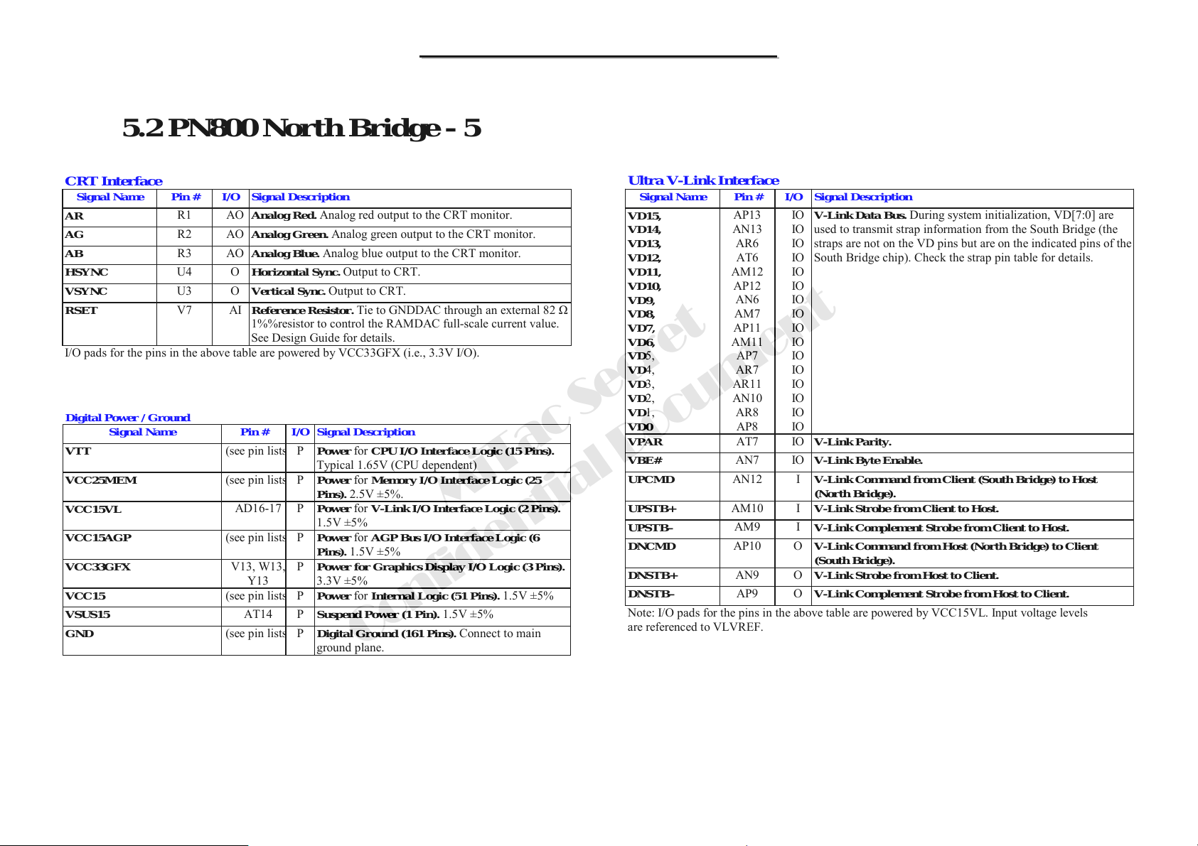
8666 N/B Maintenance
s
s
s
s
s
8666 N/B Maintenance
5.2 PN800 North Bridge - 5
CRT Interface
Signal Name Pin # I/O Signal Description
AR
AG
AB
HSYNC
VSYNC
RSET
I/O pads for the pins in the above table are powered by VCC33GFX (i.e., 3.3V I/O).
Digital Power / Ground
VTT
VCC25MEM
VCC15VL
VCC15AGP
VCC33GFX
VCC15
VSUS15
GND
Signal Name Pin # I/O Signal Description
R1 AO Analog Red. Analog red output to the CRT monitor.
R2 AO Analog Green. Analog green output to the CRT monitor.
R3 AO Analog Blue. Analog blue output to the CRT monitor.
U4 O Horizontal Sync. Output to CRT.
U3 O Vertical Sync. Output to CRT.
V7 AI Reference Resistor. Tie to GNDDAC through an external 82 Ω
1%%resistor to control the RAMDAC full-scale current value.
See Design Guide for details.
(see pin list
(see pin list
AD16-17 P Power for V-Link I/O Interface Logic (2 Pins).
(see pin list
V13, W13,
Y13
(see pin list
AT14 P Suspend Power (1 Pin). 1.5V ±5%
(see pin list
P Power for CPU I/O Interface Logic (15 Pins).
Typical 1.65V (CPU dependent)
P Power for Memory I/O Interface Logic (25
Pins). 2.5V ±5%.
MiTac Secret
1.5V ±5%
P Power for AGP Bus I/O Interface Logic (6
Pins). 1.5V ±5%
P
Power for Graphics Display I/O Logic (3 Pins).
3.3V ±5%
P Power for Internal Logic (51 Pins). 1.5V ±5%
P Digital Ground (161 Pins). Connect to main
ground plane.
Confidential Document
Ultra V- L i nk Interfac e
Signal Name Pin # I/O Signal Description
VD15,
VD14,
VD13,
VD12,
VD11,
VD10,
VD9,
VD8,
VD7,
VD6,
VD5,
VD4,
VD3,
VD2,
VD1,
VD0
VPAR
VBE#
UPCMD
UPSTB+
UPSTB–
DNCMD
DNSTB+
DNSTB–
Note: I/O pads for the pins in the above table are powered by VCC15VL. Input voltage levels
are referenced to VLVREF.
AP13
AN13
AR6
AT6
AM12
AP12
AN6
AM7
AP11
AM11
AP7
AR7
AR11
AN10
AR8
AP8
AT7 IO
AN7 IO
AN12 I
AM10 I
AM9 I
AP10 O
AN9 O
AP9 O
IO
V-Link Data Bus. During system initialization, VD[7:0] are
IO
used to transmit strap information from the South Bridge (the
IO
straps are not on the VD pins but are on the indicated pins of the
IO
South Bridge chip). Check the strap pin table for details.
IO
IO
IO
IO
IO
IO
IO
IO
IO
IO
IO
IO
V-Link Parity.
V-Link Byte Enable.
V-Link Command from Client (South Bridge) to Host
(North Bridge).
V-Link Strobe from Client to Host.
V-Link Complement Strobe from Client to Host.
V-Link Command from Host (North Bridge) to Client
(South Bridge).
V-Link Strobe from Host to Client.
V-Link Complement Strobe from Host to Client.
90
Page 92
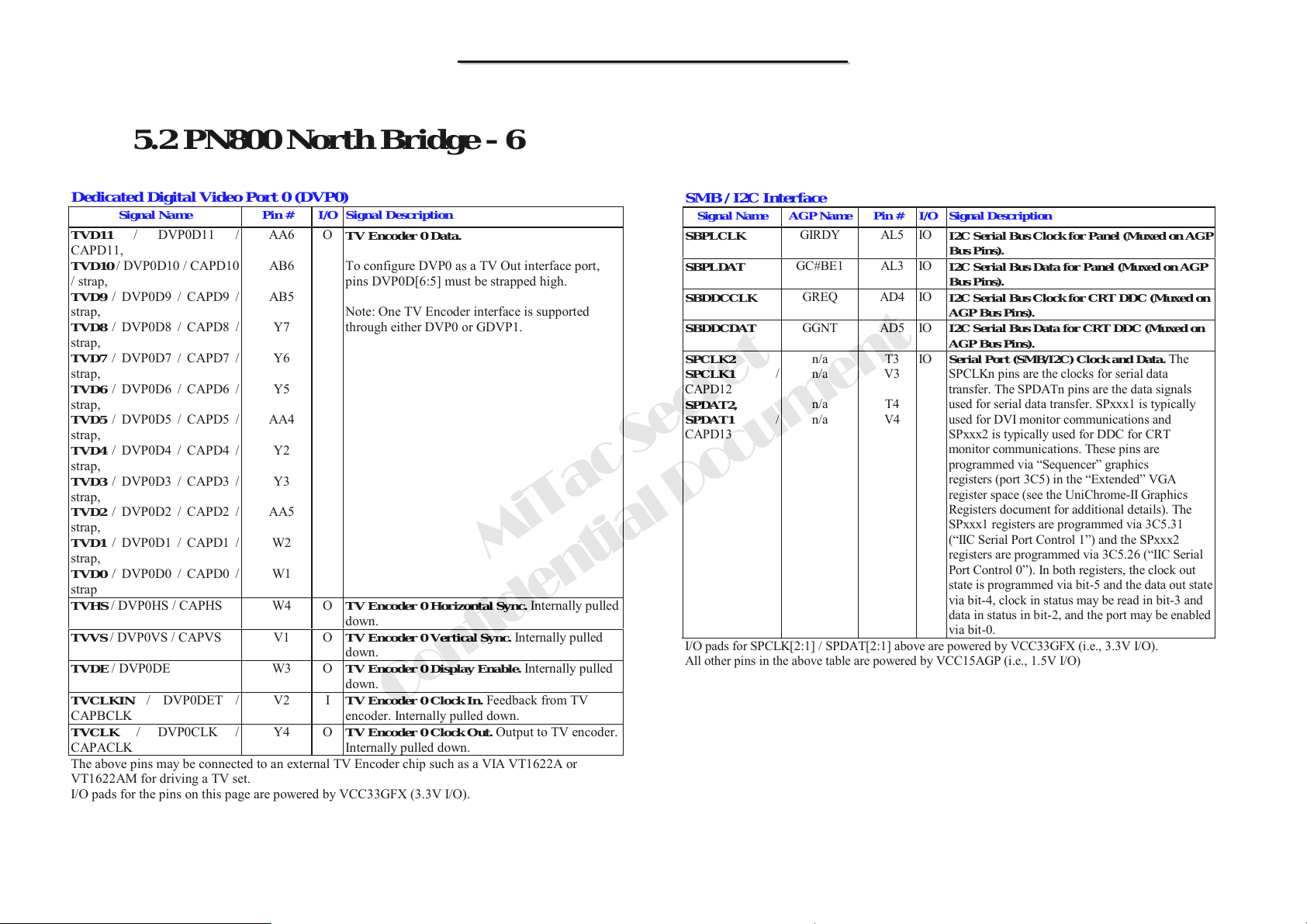
8666 N/B Maintenance
8666 N/B Maintenance
5.2 PN800 North Bridge - 6
Dedicated Digital Video Port 0 (DVP0)
Signal Name Pin # I/O Signal Description
TVD11 / DVP0D11 /
CAPD11,
TVD10 / DVP0D10 / CAPD10
/ strap,
TVD9 / DVP0D9 / CAPD9 /
strap,
TVD8 / DVP0D8 / CAPD8 /
strap,
TVD7 / DVP0D7 / CAPD7 /
strap,
TVD6 / DVP0D6 / CAPD6 /
strap,
TVD5 / DVP0D5 / CAPD5 /
strap,
TVD4 / DVP0D4 / CAPD4 /
strap,
TVD3 / DVP0D3 / CAPD3 /
strap,
TVD2 / DVP0D2 / CAPD2 /
strap,
TVD1 / DVP0D1 / CAPD1 /
strap,
TVD0 / DVP0D0 / CAPD0 /
strap
TVHS / DVP0HS / CAPHS W4 O TV Enco der 0 Hor izo ntal Sync. Internally pulled
TVVS / DVP0VS / CAPVS V1 O TV Encoder 0 Vertical Sync. Internally pulled
TVDE / DVP0DE W3 O TV Enco der 0 Displa y Enable . Internally pulled
TVCLKIN / DVP0DET /
CAPBCLK
TVCLK / DVP0CLK /
CAPACLK
The above pins may be connected to an external TV Encoder chip such as a VIA VT1622A or
VT1622AM for driving a TV set.
I/O pads for the pins on this page are powered by VCC33GFX (3.3V I/O).
AA6
AB6
AB5
Y7
Y6
Y5
AA4
Y2
Y3
AA5
W2
W1
V2 I TV Encoder 0 Clock In. Feedback from TV
Y4 O TV Encoder 0 Clock Out. Output to TV encoder.
O
TV Encoder 0 Data.
To configure DVP0 as a TV Out interface port,
pins DVP0D[6:5] must be strapped high.
Note: One TV Encoder interface is supported
through either DVP0 or GDVP1.
MiTac Secret
down.
down.
down.
Confidential Document
encoder. Internally pulled down.
Internally pulled down.
SMB / I2C Interface
Signal Name AGP Name Pin # I/O Signal Description
SBPLCLK
SBPLDAT
SBDDCCLK
SBDDCDAT
SPCLK2
SPCLK1 /
CAPD12
SPDAT2,
SPDAT1 /
CAPD13
I/O pads for SPCLK[2:1] / SPDAT[2:1] above are powered by VCC33GFX (i.e., 3.3V I/O).
All other pins in the above table are powered by VCC15AGP (i.e., 1.5V I/O)
GIRDY AL5 IO
GC#BE1 AL3 IO
GREQ AD4 IO
GGNT AD5 IO
n/a
n/a
n/a
n/a
T3
V3
T4
V4
I2C Serial Bus Clock for Panel (Muxed on AGP
Bus Pins).
I2C Serial Bus Data for Panel (Muxed on AGP
Bus Pins).
I2C Serial Bus Clock for CRT DDC (Muxed on
AGP Bus Pins).
I2C Serial Bus Data for CRT DDC (Muxed on
AGP Bus Pins).
IO Serial Port (SMB/I2C) Clock and Data. The
SPCLKn pins are the clocks for serial data
transfer. The SPDATn pins are the data signals
used for serial data transfer. SPxxx1 is typically
used for DVI monitor communications and
SPxxx2 is typically used for DDC for CRT
monitor communications. These pins are
programmed via “Sequencer” graphics
registers (port 3C5) in the “Extended” VGA
register space (see the UniChrome-II Graphics
Registers document for additional details). The
SPxxx1 registers are programmed via 3C5.31
(“IIC Serial Port Control 1”) and the SPxxx2
registers are programmed via 3C5.26 (“IIC Serial
Port Control 0”). In both registers, the clock out
state is programmed via bit-5 and the data out state
via bit-4, clock in status may be read in bit-3 and
data in status in bit-2, and the port may be enabled
via bit-0.
91
Page 93
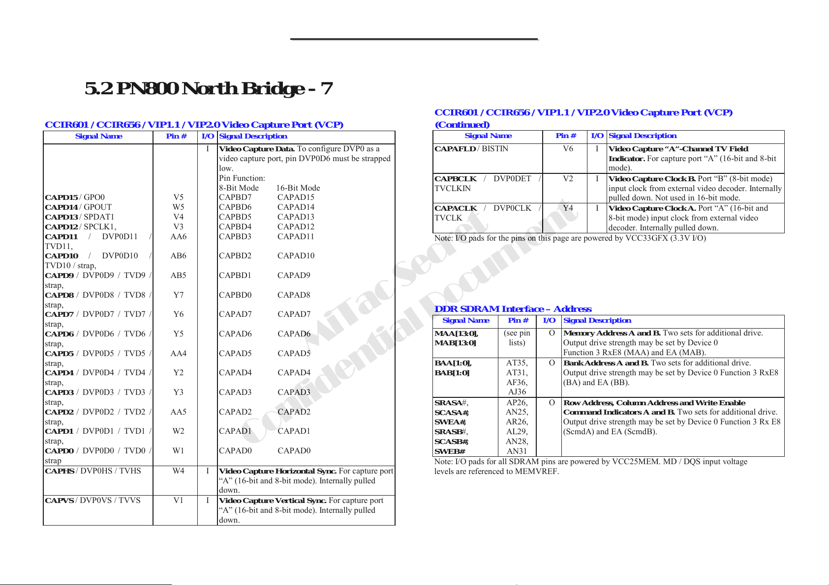
8666 N/B Maintenance
8666 N/B Maintenance
5.2 PN800 North Bridge - 7
CCIR601 / CCIR656 / VIP1.1 / VIP2.0 Video Capture Port (VCP)
Signal Name Pin # I/O Signal Description
I Video Capture Data. To configure DVP0 as a
CAPD15
CAPD14
CAPD13
CAPD12 / SPCLK1,
CAPD11 / DVP0D11 /
TVD11,
CAPD10 / DVP0D10 /
TVD10 / strap,
CAPD9 / DVP0D9 / TVD9 /
strap,
CAPD8 / DVP0D8 / TVD8 /
strap,
CAPD7 / DVP0D7 / TVD7 /
strap,
CAPD6 / DVP0D6 / TVD6 /
strap,
CAPD5 / DVP0D5 / TVD5 /
strap,
CAPD4 / DVP0D4 / TVD4 /
strap,
CAPD3 / DVP0D3 / TVD3 /
strap,
CAPD2 / DVP0D2 / TVD2 /
strap,
CAPD1
strap,
CAPD0 / DVP0D0 / TVD0 /
strap
CAPHS / DVP0HS / TVHS W4 I Video Capture Horizontal Sync. For capture port
CAPVS / DVP0VS / TVVS V1 I Video Capture Vertical Sync. For capture port
/ GPO0
/ GPOUT
/ SPDAT1
/ DVP0D1 / TVD1 /
V5
W5
V4
V3
AA6
AB6
AB5
Y7
Y6
Y5
AA4
Y2
Y3
AA5
W2
W1
video capture port, pin DVP0D6 must be strapped
low.
Pin Function:
8-Bit Mode 16-Bit Mode
CAPBD7 CAPAD15
CAPBD6 CAPAD14
CAPBD5 CAPAD13
CAPBD4 CAPAD12
CAPBD3 CAPAD11
CAPBD2 CAPAD10
CAPBD1 CAPAD9
CAPBD0 CAPAD8
CAPAD7 CAPAD7
CAPAD6 CAPAD6
CAPAD5 CAPAD5
CAPAD4 CAPAD4
CAPAD3 CAPAD3
CAPAD2 CAPAD2
CAPAD1 CAPAD1
CAPAD0 CAPAD0
“A” (16-bit and 8-bit mode). Internally pulled
down.
“A” (16-bit and 8-bit mode). Internally pulled
down.
Confidential Document
MiTac Secret
CCIR601 / CCIR656 / VIP1.1 / VIP2.0 Video Capture Port (VCP)
(Continued)
Signal Name Pin # I/O Signal Description
CAPAFLD / BISTIN V6 I
CAPBCLK / DVP0DET /
TVCLKIN
CAPACLK / DVP0CLK /
TVCLK
Note: I/O pads for the pins on this page are powered by VCC33GFX (3.3V I/O)
V2 I Video Capture Clock B. Port “B” (8-bit mode)
Y4 I Video Capture Clock A. Port “A” (16-bit and
Video Capture “A”-Channel TV Field
Indicator. For capture port “A” (16-bit and 8-bit
mode).
input clock from external video decoder. Internally
pulled down. Not used in 16-bit mode.
8-bit mode) input clock from external video
decoder. Internally pulled down.
DDR SDRAM Interface – Address
Signal Name Pin # I/O Signal Description
MAA[13:0],
MAB[13:0]
BAA[1:0],
BAB[1:0]
SRASA#,
SCASA#,
SWEA#,
SRASB#,
SCASB#,
SWEB#
Note: I/O pads for all SDRAM pins are powered by VCC25MEM. MD / DQS input voltage
levels are referenced to MEMVREF.
(see pin
lists)
AT35,
AT31,
AF36,
AJ36
AP26,
AN25,
AR26,
AL29,
AN28,
AN31
O Memory Address A and B. Two sets for additional drive.
Output drive strength may be set by Device 0
Function 3 RxE8 (MAA) and EA (MAB).
O Bank Address A and B. Two sets for additional drive.
Output drive strength may be set by Device 0 Function 3 RxE8
(BA) and EA (BB).
O
Row Address, Column Address and Write Enable
Command Indicators A and B. Two sets for additional drive.
Output drive strength may be set by Device 0 Function 3 Rx E8
(ScmdA) and EA (ScmdB).
92
Page 94
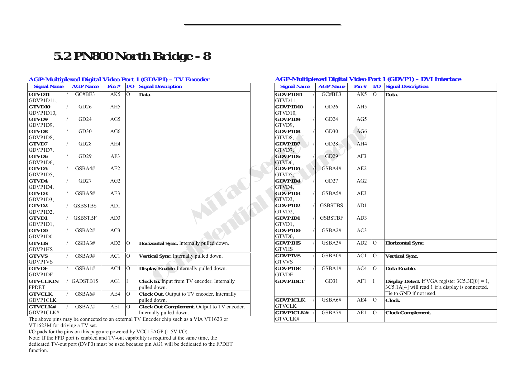
8666 N/B Maintenance
8666 N/B Maintenance
5.2 PN800 North Bridge - 8
AGP-Multiplexed Digital Video Port 1 (GDVP1) – TV Encoder
Signal Name AGP Name Pin # I/O Signal Description
O
GTVD11 /
GDVP1D11,
GTVD10 /
GDVP1D10,
GTVD9 /
GDVP1D9,
GTVD8 /
GDVP1D8,
GTVD7 /
GDVP1D7,
GTVD6 /
GDVP1D6,
GTVD5 /
GDVP1D5,
GTVD4 /
GDVP1D4,
GTVD3 /
GDVP1D3,
GTVD2
GDVP1D2,
GTVD1
GDVP1D1,
GTVD0 /
GDVP1D0
GTVHS /
GDVP1HS
GTVVS /
GDVP1VS
GTVDE /
GDVP1DE
GTVCLKIN /
FPDET
GTVCLK
GDVP1CLK
GTVCLK# /
GDVP1CLK#
The above pins may be connected to an external TV Encoder chip such as a VIA VT1623 or
VT1623M for driving a TV set.
I/O pads for the pins on this page are powered by VCC15AGP (1.5V I/O).
Note: If the FPD port is enabled and TV-out capability is required at the same time, the
dedicated TV-out port (DVP0) must be used because pin AG1 will be dedicated to the FPDET
function.
GC#BE3
GD26
GD24
GD30
GD28
GD29
GSBA4#
GD27
GSBA5#
GSBSTBS
/
GSBSTBF
/
GSBA2#
GSBA3# AD2 O Horizontal Sync. Internally pulled down.
GSBA0# AC1 O Vertical Sync. Internally pulled down.
GSBA1# AC4 O Display Enable. Internally pulled down.
GADSTB1S AG1 I Clock In. Input from TV encoder. Internally
/
GSBA6# AE4 O
GSBA7# AE1 O Clock Out Complement. Output to TV encoder.
AK5
AH5
AG5
AG6
AH4
AF3
AE2
AG2
AE3
AD1
AD3
AC3
Data.
Confidential Document
pulled down.
Clock Out.
pulled down.
Internally pulled down.
Output to TV encoder. Internally
MiTac Secret
AGP-Multiplexed Digital Video Port 1 (GDVP1) – DVI Interface
Signal Name AGP Name Pin # I/O Signal Description
O
GDVP1D11 /
GTVD11,
GDVP1D10 /
GTVD10,
GDVP1D9 /
GTVD9,
GDVP1D8 /
GTVD8,
GDVP1D7 /
GTVD7,
GDVP1D6 /
GTVD6,
GDVP1D5
GTVD5,
GDVP1D4 /
GTVD4,
GDVP1D3 /
GTVD3,
GDVP1D2 /
GTVD2,
GDVP1D1 /
GTVD1,
GDVP1D0 /
GTVD0,
GDVP1HS /
GTVHS
GDVP1VS /
GTVVS
GDVP1DE /
GTVDE
GDVP1DET
GDVP1CLK
GTVCLK
GDVP1CLK# /
GTVCLK#
GC#BE3
GD26
GD24
GD30
GD28
GD29
GSBA4#
/
/
GD27
GSBA5#
GSBSTBS
GSBSTBF
GSBA2#
GSBA3# AD2 O
GSBA0# AC1 O
GSBA1# AC4 O
GD31 AF1 I Display Detect. If VGA register 3C5.3E[0] = 1,
GSBA6# AE4 O
GSBA7# AE1 O
AK5
AH5
AG5
AG6
AH4
AF3
AE2
AG2
AE3
AD1
AD3
AC3
Data.
Horizontal Sync.
Vertical Sync.
Data Enable.
3C5.1A[4] will read 1 if a display is connected.
Tie to GND if not used.
Clock.
Clock Complement.
93
Page 95
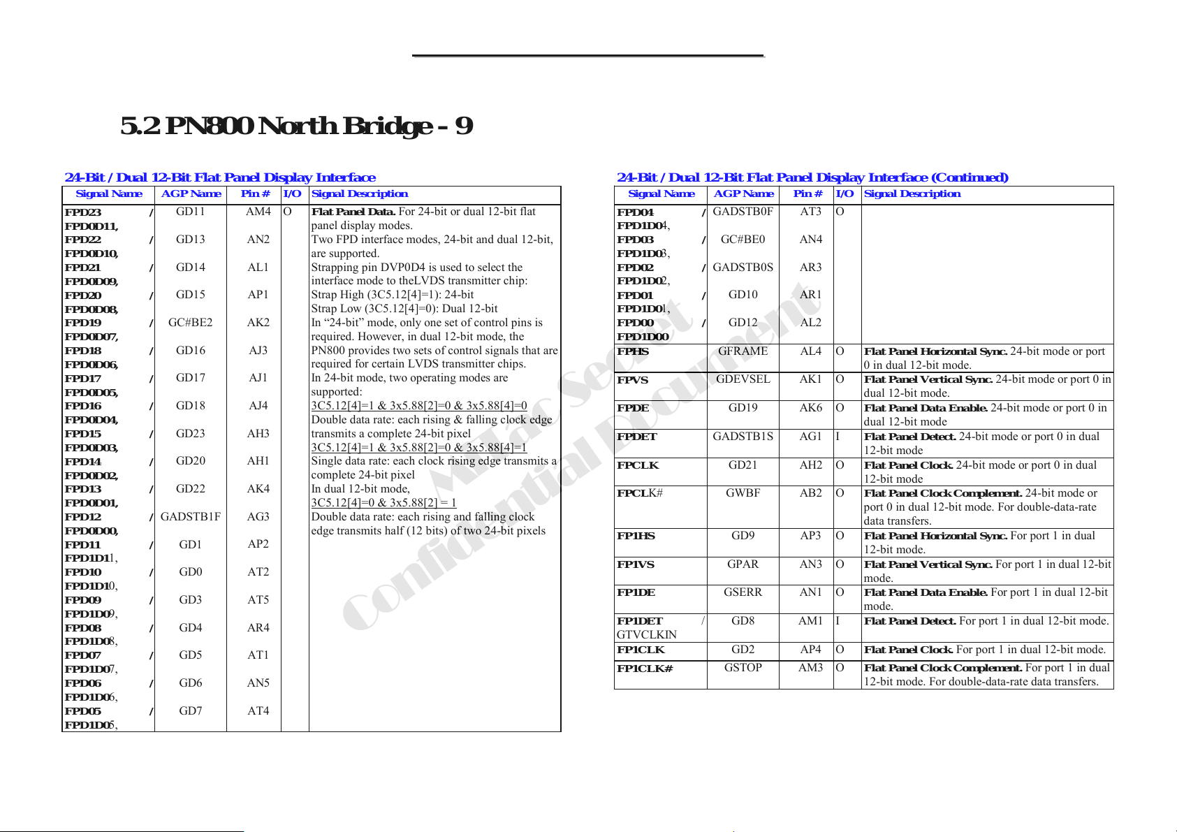
8666 N/B Maintenance
b
b
8666 N/B Maintenance
5.2 PN800 North Bridge - 9
24-Bit / Dual 12-Bit Flat Panel Display Interface
Signal Name AGP Name Pin # I/O Signal Description
O Flat Panel Data. For 24-bit or dual 12-bit flat
FPD23 /
FPD0D11,
FPD22 /
FPD0D10,
FPD21 /
FPD0D09,
FPD20 /
FPD0D08,
FPD19 /
FPD0D07,
FPD18 /
FPD0D06,
FPD17 /
FPD0D05,
FPD16 /
FPD0D04,
FPD15 /
FPD0D03,
FPD14 /
FPD0D02,
FPD13 /
FPD0D01,
FPD12 /
FPD0D00,
FPD11 /
FPD1D11,
FPD10 /
FPD1D10,
FPD09 /
FPD1D09,
FPD08 /
FPD1D08,
FPD07 /
FPD1D07,
FPD06 /
FPD1D06,
FPD05 /
FPD1D05,
GD11
GD13
GD14
GD15
GC#BE2
GD16
GD17
GD18
GD23
GD20
GD22
GADSTB1F
GD1
GD0
GD3
GD4
GD5
GD6
GD7
AM4
AN2
AL1
AP1
AK2
AJ3
AJ1
AJ4
AH3
AH1
AK4
AG3
AP2
AT2
AT5
AR4
AT1
AN5
AT4
panel display modes.
Two FPD interface modes, 24-bit and dual 12-bit,
are supported.
Strapping pin DVP0D4 is used to select the
interface mode to theLVDS transmitter chip:
Strap High (3C5.12[4]=1): 24-bit
Strap Low (3C5.12[4]=0): Dual 12-bit
In “24-bit” mode, only one set of control pins is
required. However, in dual 12-bit mode, the
PN800 provides two sets of control signals that are
required for certain LVDS transmitter chips.
In 24-bit mode, two operating modes are
supported:
3C5.12[4]=1 & 3x5.88[2]=0 & 3x5.88[4]=0
Double data rate: each rising & falling clock edge
transmits a complete 24-bit pixel
3C5.12[4]=1 & 3x5.88[2]=0 & 3x5.88[4]=1
Single data rate: each clock rising edge transmits a
complete 24-bit pixel
In dual 12-bit mode,
3C5.12[4]=0 & 3x5.88[2] = 1
Double data rate: each rising and falling clock
edge transmits half (12 bits) of two 24-bit pixels
Confidential Document
24-Bit / Dual 12-Bit Flat Panel Display Interface (Continued)
Signal Name AGP Name Pin # I/O Signal Description
FPD04 /
FPD1D04,
FPD03 /
FPD1D03,
FPD02 /
FPD1D0
FPD01 /
FPD1D01,
FPD00 /
FPD1D00
FPHS
FPVS
MiTac Secret
FPDE
FPDET
FPCLK
FPCLK# GWBF AB2 O Flat Panel Clock Complement. 24-bit mode or
FP1HS
FP1VS
FP1DE
FP1DET /
GTVCLKIN
FP1CLK
FP1CLK#
2,
GADSTB0F
GC#BE0
GADSTB0S
GD10
GD12
GFRAME AL4 O Flat Panel Horizontal Sync. 24-bit mode or port
GDEVSEL AK1 O Flat Panel Vertical Sync. 24-
GD19 AK6 O Flat Panel Data Enable. 24-bit mode or port 0 in
GADSTB1S AG1 I Flat Panel Detect. 24-bit mode or port 0 in dual
GD21 AH2 O
GD9 AP3 O Flat Panel Horizontal Sync. For port 1 in dual
GPAR AN3 O Flat Panel Vertical Sync. For port 1 in dual 12-
GSERR AN1 O Flat Panel Data Enable. For port 1 in dual 12-bit
GD8 AM1 I Flat Panel Detect. For port 1 in dual 12-bit mode.
GD2 AP4 O Flat Pane l Cloc k. For port 1 in dual 12-bit mode.
GSTOP AM3 O Flat Panel Clock Complement. For port 1 in dual
O
AT3
AN4
AR3
AR1
AL2
0 in dual 12-bit mode.
dual 12-bit mode.
dual 12-bit mode
12-bit mode
Flat Panel Clock.
12-bit mode
port 0 in dual 12-bit mode. For double-data-rate
data transfers.
12-bit mode.
mode.
mode.
12-bit mode. For double-data-rate data transfers.
24-bit mode or port 0 in dual
it mode or port 0 in
it
94
Page 96
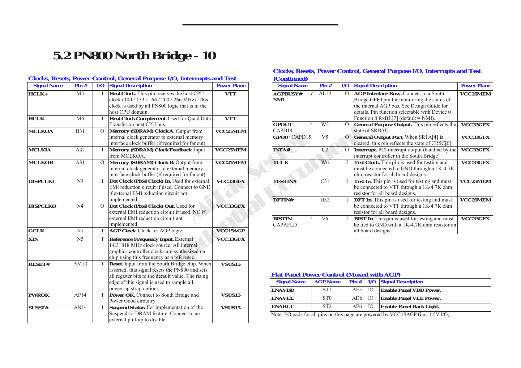
8666 N/B Maintenance
8666 N/B Maintenance
5.2 PN800 North Bridge - 10
Clocks, Resets, Power Control, General Purpose I/O, Interrupts and Test
Signal Name Pin # I/O Signal Description Power Plane
HCLK+
HCLK–
MCLKOA
MCLKIA
MCLKOB
DISPCLKI
DISPCLKO
GCLK
XIN
RESET#
PWROK
SUSST#
M5 I Host Clock. This pin receives the host CPU
M6 I Host Clock Complement. Used for Quad Data
B31 O
A32 I Memory (SDRAM) Clock Feedback. Input
A31 O Memory (SDRAM) Clock B. Output from
N3 I
N4 O Dot Clock (Pixel Clock) Out. Used for
N7 I AGP Clock. Clock for AGP logic.
N5 I Reference Frequency Input. External
AM13 I
AP14 I Power OK. Connect to South Bridge and
AN14 I Suspend Status. For implementation of the
clock (100 / 133 / 166 / 200 / 266 MHz). This
clock is used by all PN800 logic that is in the
host CPU domain.
Transfer on host CPU bus.
Memory (SDRAM) Clock A.
internal clock generator to external memory
interface clock buffer (if required for fanout)
from MCLKOA.
internal clock generator to external memory
interface clock buffer (if required for fanout)
Dot Clock (Pixel Clock) In.
EMI reduction circuit if used. Connect to GND
if external EMI reduction circuit not
implemented.
external EMI reduction circuit if used. NC if
external EMI reduction circuit not
implemented.
14.31818 MHz clock source. All internal
graphics controller clocks are synthesized on
chip using this frequency as a reference.
Reset.
Input from the South Bridge chip. When
asserted, this signal resets the PN800 and sets
all register bits to the default value. The rising
edge of this signal is used to sample all
power-up strap options
Power Good circuitry.
Suspend-to-DRAM feature. Connect to an
external pull-up to disable.
Confidential Document
Output from
Used for external
MiTac Secret
VTT
VTT
VCC25MEM
VCC25MEM
VCC25MEM
VCC33GFX
VCC33GFX
VCC15AGP
VCC33GFX
VSUS15
VSUS15
VSUS15
Clocks, Resets, Power Control, General Purpose I/O, Interrupts and Test
(Continued)
Signal Name Pin # I/O Signal Description Power Plane
AGPBUSY# /
NMI
GPOUT /
CAPD14
GPO0 / CAPD15 V5 O General Output Port. When SR1A[4] is
INTA#
TCLK
TESTIN#
DFTIN#
BISTIN
CAPAFLD
AL14 O
W5 O General Purpose Output. This pin reflects the
U2 O Interrupt. PCI interrupt output (handled by the
W6 I Test Clock. This pin is used for testing and
C31 I Test In. This pin is used for testing and must
D32 I DFT In. This pin is used for testing and must
/
V6 I
AGP Interface Busy.
Bridge GPIO pin for monitoring the status of
the internal AGP bus. See Design Guide for
details. Pin function selectable with Device 0
Function 0 RxBE[7] (default = NMI).
state of SRD[0].
cleared, this pin reflects the state of CR5C[0].
interrupt controller in the South Bridge)
must be connected to GND through a 1K-4.7K
ohm resistor for all board designs.
be connected to VTT through a 1K-4.7K ohm
resistor for all board designs.
be connected to VTT through a 1K-4.7K ohm
resistor for all board designs.
BIST In.
be tied to GND with a 1K-4.7K ohm resistor on
all board designs.
This pin is used for testing and must
Connect to a South
VCC25MEM
VCC33GFX
VCC33GFX
VCC33GFX
VCC33GFX
VCC25MEM
VCC25MEM
VCC33GFX
Flat Panel Power Control (Muxed with AGP)
Signal Name AGP Name Pin # I/O Signal Description
ENAVDD
ENAVEE
ENABLT
Note: I/O pads for all pins on this page are powered by VCC15AGP (i.e., 1.5V I/O).
ST1 AE5 IO
ST0 AD6 IO
ST2 AE6 IO
Enable Panel VDD Power.
Enable Panel VEE Power.
Enable Panel Back Light.
95
Page 97
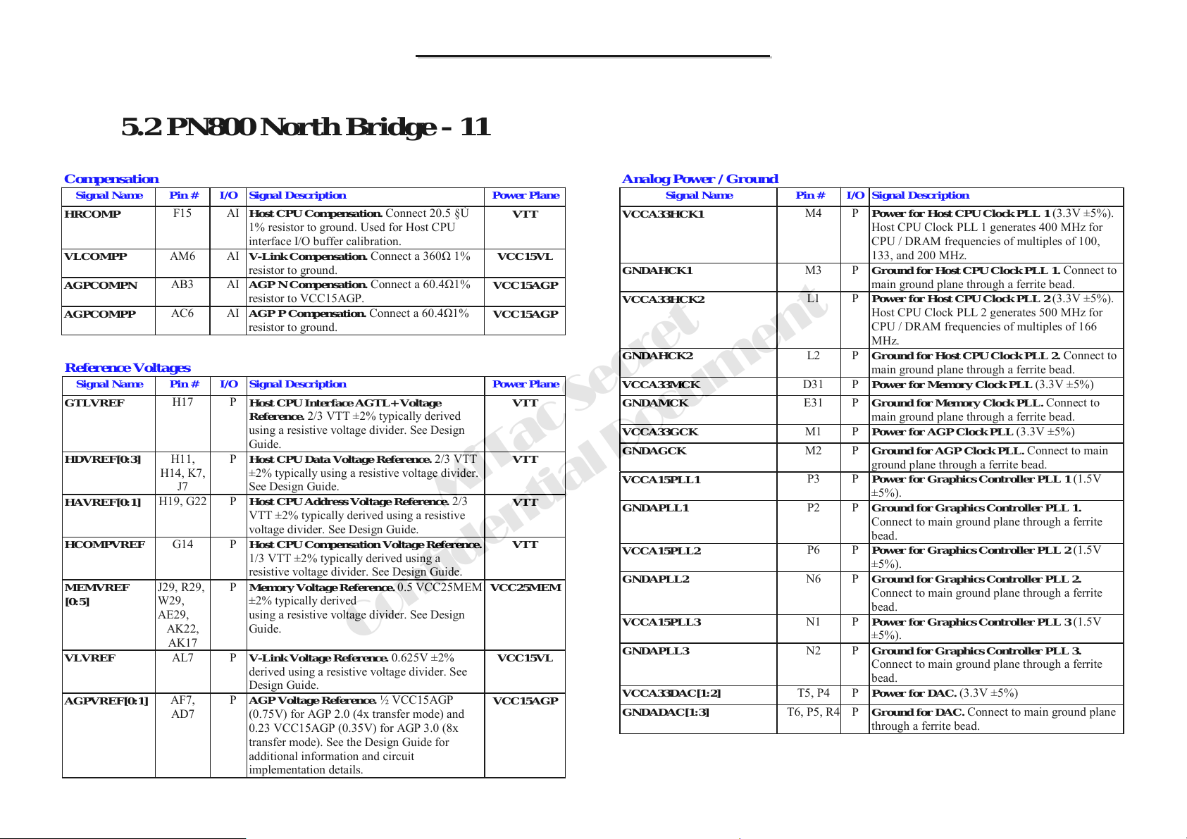
8666 N/B Maintenance
8666 N/B Maintenance
5.2 PN800 North Bridge - 11
Compensation
Signal Name Pin # I/O Signal Description Power Plane
HRCOMP
VLCOMPP
AGPCOMPN
AGPCOMPP
F15 AI Host CPU Compensation. Connect 20.5 §Ù
1% resistor to ground. Used for Host CPU
interface I/O buffer calibration.
AM6 AI V-Link Compensation. Connect a 360Ω 1%
resistor to ground.
AB3 AI AGP N Compensation. Connect a 60.4Ω1%
resistor to VCC15AGP.
AC6 AI AGP P Compensation. Connect a 60.4Ω1%
resistor to ground.
VTT
VCC15VL
VCC15AGP
VCC15AGP
Reference Voltages
Signal Name Pin # I/O Signal Description Power Plane
GTLVREF
HDVREF[0:3]
HAVREF[0:1]
HCOMPVREF
MEMVREF
[0:5]
VLVREF
AGPVREF[0:1]
H17 P
H11,
H14, K7,
J7
H19, G22 P Host CPU Address Voltage Reference. 2/3
G14 P
J29, R29,
W29,
AE29,
AK22,
AK17
AL7 P V-Link Voltage Reference. 0.625V ±2%
AF7,
AD7
Host CPU Interface AGTL+ Voltage
Reference. 2/3 VTT ±2% typically derived
using a resistive voltage divider. See Design
Guide.
P Host CPU Data Volt age Referen c e. 2/3 VTT
±2% typically using a resistive voltage divider.
See Design Guide.
MiTac Secret
VTT ±2% typically derived using a resistive
voltage divider. See Design Guide.
Host CPU Compensation Voltage Reference.
1/3 VTT ±2% typically derived using a
resistive voltage divider. See Design Guide.
P Memory Voltage Reference. 0.5 VCC25MEM
±2% typically derived
using a resistive voltage divider. See Design
Guide.
derived using a resistive voltage divider. See
Design Guide.
P AGP Voltage Reference. ½ VCC15AGP
(0.75V) for AGP 2.0 (4x transfer mode) and
0.23 VCC15AGP (0.35V) for AGP 3.0 (8x
transfer mode). See the Design Guide for
additional information and circuit
implementation details.
Confidential Document
VTT
VTT
VTT
VTT
VCC25MEM
VCC15VL
VCC15AGP
Analog Power / Ground
Signal Name Pin # I/O Signal Description
VCCA33HCK1
GNDAHCK1
VCCA33HCK2
GNDAHCK2
VCCA33MCK
GNDAMCK
VCCA33GCK
GNDAGCK
VCCA15PLL1
GNDAPLL1
VCCA15PLL2
GNDAPLL2
VCCA15PLL3
GNDAPLL3
VCCA33DAC[1:2]
GNDADAC[1:3]
M4 P Power for Host CPU Clock PLL 1 (3.3V ±5%).
M3 P Ground for Host CPU Clock PLL 1. Connect to
L1 P Power for Host CPU Clock PLL 2 (3.3V ±5%).
L2 P Ground for Host CPU Clock PLL 2. Connect to
D31 P Power for Memory Clock PLL (3.3V ±5%)
E31 P Ground for Memory Clock PLL. Connect to
M1 P Power for AGP Clock PLL (3.3V ±5%)
M2 P Ground for AGP Clock PLL. Connect to main
P3 P Power for Graphics Controller PLL 1 (1.5V
P2 P
P6 P Power for Graphics Controller PLL 2 (1.5V
N6 P
N1 P
N2 P
T5, P4 P Power for DAC. (3.3V ±5%)
T6, P5, R4 P Ground for DAC. Connect to main ground plane
Host CPU Clock PLL 1 generates 400 MHz for
CPU / DRAM frequencies of multiples of 100,
133, and 200 MHz.
main ground plane through a ferrite bead.
Host CPU Clock PLL 2 generates 500 MHz for
CPU / DRAM frequencies of multiples of 166
MHz.
main ground plane through a ferrite bead.
main ground plane through a ferrite bead.
ground plane through a ferrite bead.
±5%).
Ground for Graphics Controller PLL 1.
Connect to main ground plane through a ferrite
bead.
±5%).
Ground for Graphics Controller PLL 2.
Connect to main ground plane through a ferrite
bead.
Power for Graphics Controller PLL 3
±5%).
Ground for Graphics Controller PLL 3.
Connect to main ground plane through a ferrite
bead.
through a ferrite bead.
(1.5V
96
Page 98
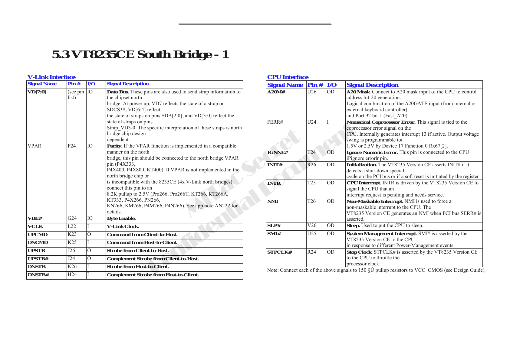
8666 N/B Maintenance
8666 N/B Maintenance
5.3 VT8235CE South Bridge - 1
V-Link Interface
Signal Name Pin # I/O Signal Description
VD[7:0]
VPAR F24 IO Parity. If the VPAR function is implemented in a compatible
VBE#
VCLK
UPCMD
DNCMD
UPSTB
UPSTB#
DNSTB
DNSTB#
(see pin
list)
G24 IO
L22 I
K23 O
K25 I
J26 O
J24 O
K26 I
H24 I
IO Data Bus. These pins are also used to send strap information to
the chipset north
bridge. At power up, VD7 reflects the state of a strap on
SDCS3#, VD[6:4] reflect
the state of straps on pins SDA[2:0], and VD[3:0] reflect the
state of straps on pins
Strap_VD3-0. The specific interpretation of these straps is north
bridge chip design
dependent.
manner on the north
bridge, this pin should be connected to the north bridge VPAR
pin (P4X333,
P4X400, P4X800, KT400). If VPAR is not implemented in the
north bridge chip or
is incompatible with the 8235CE (4x V-Link north bridges)
connect this pin to an
8.2K pullup to 2.5V (Pro266, Pro266T, KT266, KT266A,
KT333, P4X266, PN266,
KN266, KM266, P4M266, P4N266). See app note AN222 for
details.
Byte Enable.
V-Link Clock.
Command from Client-to-Host.
Command from Host-to-Client.
Strobe from Client-to-Host.
Complement Strobe from Client-to-Host.
Strobe from Host-to-Client.
Complement Strobe from Host-to-Client.
Confidential Document
MiTac Secret
CPU Interface
Signal Name Pin # I/O Signal Description
A20M#
FERR# U24 I Numerical Coprocessor Error. This signal is tied to the
IGNNE#
INIT#
INTR
NMI
SLP#
SMI#
STPCLK#
Note: Connect each of the above signals to 150 §Ù pullup resistors to VCC_CMOS (see Design Guide).
U26 OD A20 Mask. Connect to A20 mask input of the CPU to control
T24 OD Ignore Numeric Error. This pin is connected to the CPU
R26 OD
T25 OD CPU Interrupt. INTR is driven by the VT8235 Version CE to
T26 OD Non-Maskable Interrupt. NMI is used to force a
V26 OD Sleep. Used to put the CPU to sleep.
U25 OD System Management Interrupt. SMI# is asserted by the
R24 OD Stop Clock. STPCLK# is asserted by the VT8235 Version CE
address bit-20 generation.
Logical combination of the A20GATE input (from internal or
external keyboard controller)
and Port 92 bit-1 (Fast_A20).
coprocessor error signal on the
CPU. Internally generates interrupt 13 if active. Output voltage
swing is programmable tot
1.5V or 2.5V by Device 17 Function 0 Rx67[2].
iPignore errorlr pin.
Initialization.
detects a shut-down special
cycle on the PCI bus or if a soft reset is initiated by the register
signal the CPU that an
interrupt request is pending and needs service.
non-maskable interrupt to the CPU. The
VT8235 Version CE generates an NMI when PCI bus SERR# is
asserted.
VT8235 Version CE to the CPU
in response to different Power-Management events.
to the CPU to throttle the
processor clock.
The VT8235 Version CE asserts INIT# if it
97
Page 99
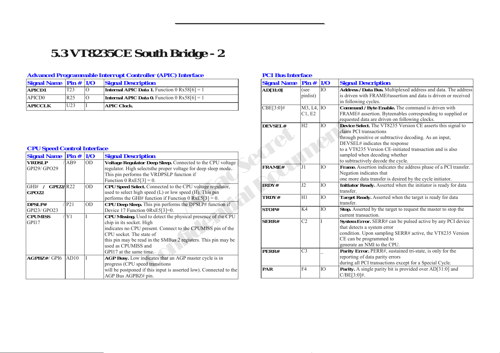
8666 N/B Maintenance
8666 N/B Maintenance
5.3 VT8235CE South Bridge - 2
Advanced Programmable Interrupt Controller (APIC) Interface
Signal Name Pin # I/O Signal Description
APICD1
APICD0 R25 O Internal APIC Data 0. Function 0 Rx58[6] = 1
APICCLK
T23 O
U23 I
Internal APIC Data 1.
APIC Clock.
Function 0 Rx58[6] = 1
CPU Speed Control Interface
Signal Name Pin # I/O Signal Description
VRDSLP /
GPI29/ GPO29
GHI# / GPI22/
GPO22
DPSLP# /
GPI23/ GPO23
CPUMISS /
GPI17
AGPBZ# / GPI6 AD10 I AGP Busy. Low indicates that an AGP master cycle is in
AB9 OD Voltage Regulator Deep Sleep. Connected to the CPU voltage
R22 OD CPU Speed Select. Connected to the CPU voltage regulator,
P21 OD CPU Dee p Sleep. This pin performs the DPSLP# function if
Y1 I CPU Mis s ing. Used to detect the physical presence of the CPU
regulator. High selectsthe proper voltage for deep sleep mode.
This pin performs the VRDPSLP function if
Function 0 RxE5[3] = 0.
used to select high speed (L) or low speed (H). This pin
performs the GHI# function if Function 0 RxE5[3] = 0.
Device 17 Function 0RxE5[3]=0.
chip in its socket. High
indicates no CPU present. Connect to the CPUMISS pin of the
CPU socket. The state of
this pin may be read in the SMBus 2 registers. This pin may be
used as CPUMISS and
GPI17 at the same time.
progress (CPU speed transitions
will be postponed if this input is asserted low). Connected to the
AGP Bus AGPBZ# pin.
Confidential Document
MiTac Secret
PCI Bus Interface
Signal Name Pin # I/O Signal Description
AD[31:0]
CBE[3:0]# M3, L4,
DEVSEL#
FRAME#
IRDY#
TRDY#
STOP#
SERR#
PERR#
PAR
(see
pinlist)
C1, E2
H2 IO Device Select. The VT8235 Version CE asserts this signal to
J1 IO Frame. Assertion indicates the address phase of a PCI transfer.
J2 IO Initiator Re ady. Asserted when the initiator is ready for data
H1 IO Target Ready. Asserted when the target is ready for data
K4 IO Stop. Asserted by the target to request the master to stop the
C2 I System Error. SERR# can be pulsed active by any PCI device
C3 _
F4 IO Parity. A single parity bit is provided over AD[31:0] and
IO Address / Data Bus. Multiplexed address and data. The address
IO Command / Byte Enable. The command is driven with
is driven with FRAME#assertion and data is driven or received
in following cycles.
FRAME# assertion. Byteenables corresponding to supplied or
requested data are driven on following clocks.
claim PCI transactions
through positive or subtractive decoding. As an input,
DEVSEL# indicates the response
to a VT8235 Version CE-initiated transaction and is also
sampled when decoding whether
to subtractively decode the cycle.
Negation indicates that
one more data transfer is desired by the cycle initiator.
transfer.
transfer.
current transaction.
that detects a system error
condition. Upon sampling SERR# active, the VT8235 Version
CE can be programmed to
generate an NMI to the CPU.
Parity Error.
reporting of data parity errors
during all PCI transactions except for a Special Cycle.
C/BE[3:0]#.
PERR#, sustained tri-state, is only for the
98
Page 100
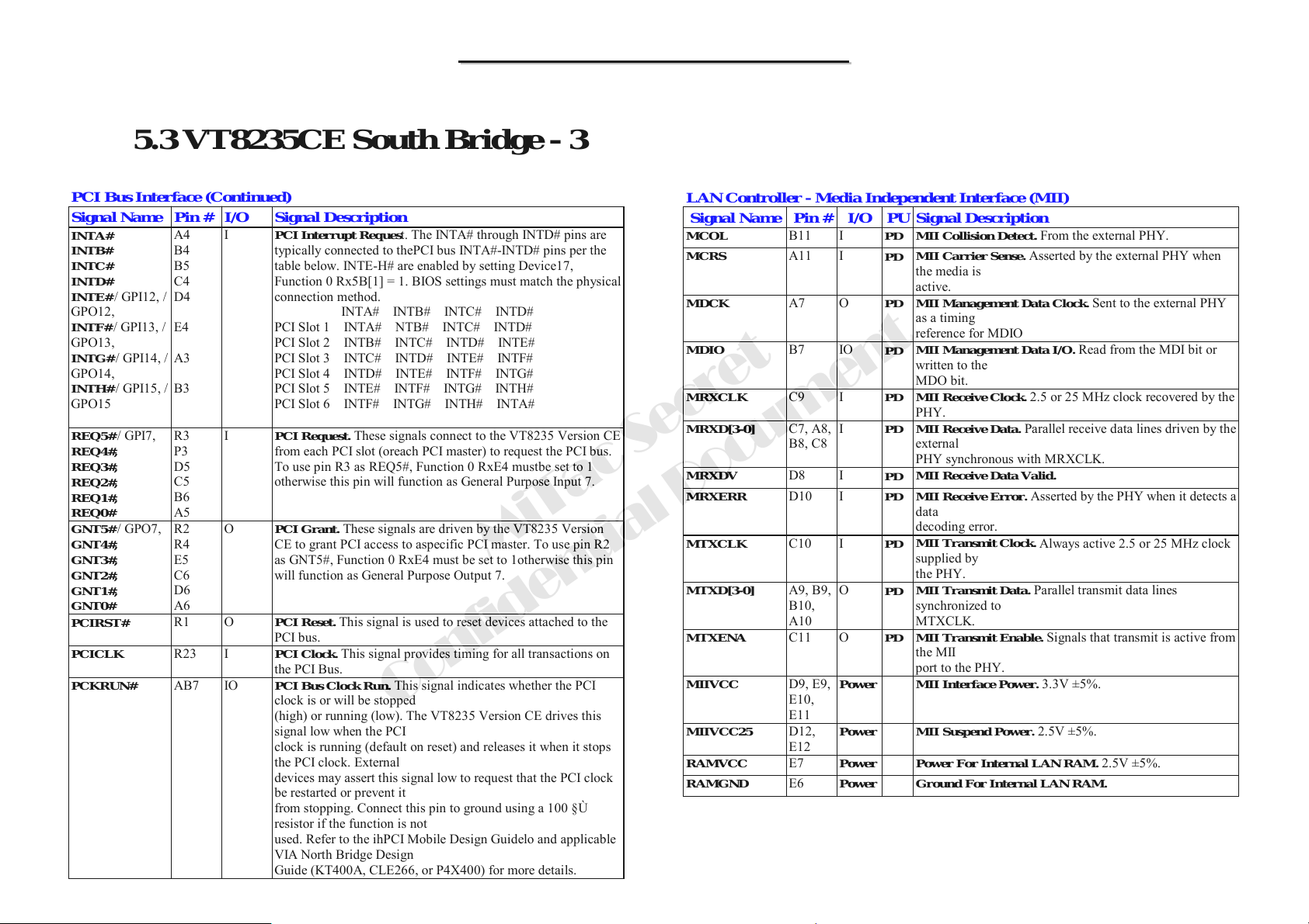
8666 N/B Maintenance
8666 N/B Maintenance
5.3 VT8235CE South Bridge - 3
PCI Bus Interface (Continued)
Signal Name Pin # I/O Signal Description
INTA#
INTB#
INTC#
INTD#
INTE# / GPI12, /
GPO12,
INTF#
/ GPI13, /
GPO13,
INTG# / GPI14, /
GPO14,
INTH# / GPI15, /
GPO15
REQ5#
REQ4#,
REQ3#,
REQ2#,
REQ1#,
REQ0#
GNT5# / GPO7,
GNT4#,
GNT3#,
GNT2#,
GNT1#,
GNT0#
PCIRST#
PCICLK
PCKRUN#
/ GPI7,
A4
B4
B5
C4
D4
E4
A3
B3
R3
P3
D5
C5
B6
A5
R2
R4
E5
C6
D6
A6
R1 O PCI Reset. This signal is used to reset devices attached to the
R23 I PCI Clock. This signal provides timing for all transactions on
AB7 IO PCI Bus Clock Run. This signal indicates whether the PCI
I PCI Interrupt Request. The INTA# through INTD# pins are
I
O PCI Grant. These signals are driven by the VT8235 Version
typically connected to thePCI bus INTA#-INTD# pins per the
table below. INTE-H# are enabled by setting Device17,
Function 0 Rx5B[1] = 1. BIOS settings must match the physical
connection method.
PCI Slot 1 INTA# NTB# INTC# INTD#
PCI Slot 2 INTB# INTC# INTD# INTE#
PCI Slot 3 INTC# INTD# INTE# INTF#
PCI Slot 4 INTD# INTE# INTF# INTG#
PCI Slot 5 INTE# INTF# INTG# INTH#
PCI Slot 6 INTF# INTG# INTH# INTA#
PCI Request.
from each PCI slot (oreach PCI master) to request the PCI bus.
To use pin R3 as REQ5#, Function 0 RxE4 mustbe set to 1
otherwise this pin will function as General Purpose Input 7.
CE to grant PCI access to aspecific PCI master. To use pin R2
as GNT5#, Function 0 RxE4 must be set to 1otherwise this pin
will function as General Purpose Output 7.
PCI bus.
the PCI Bus.
clock is or will be stopped
(high) or running (low). The VT8235 Version CE drives this
signal low when the PCI
clock is running (default on reset) and releases it when it stops
the PCI clock. External
devices may assert this signal low to request that the PCI clock
be restarted or prevent it
from stopping. Connect this pin to ground using a 100 §Ù
resistor if the function is not
used. Refer to the ihPCI Mobile Design Guidelo and applicable
VIA North Bridge Design
Guide (KT400A, CLE266, or P4X400) for more details.
INTA# INTB# INTC# INTD#
These signals connect to the VT8235 Version CE
Confidential Document
LAN Controller - Media Independent Interface (MII)
Signal Name Pin # I/O PU Signal Description
MCOL
MCRS
MDCK
MDIO
MRXCLK
MRXD[3-0]
MRXDV
MRXERR
MiTac Secret
MTXCLK
MTXD[3-0]
MTXENA
MIIVCC
MIIVCC25
RAMVCC
RAMGND
B11 I
A11 I
A7 O
B7 IO
C9 I
C7, A8,
B8, C8
D8 I
D10 I
C10 I
A9, B9,
B10,
A10
C11 O
D9, E9,
E10,
E11
D12,
E12
E7
E6
I
O
Power
Power
Power
Power
MII Collision Detect. From the external PHY.
PD
MII Carrier Sense. Asserted by the external PHY when
PD
the media is
active.
MII Management Data Clock. Sent to the external PHY
PD
as a timing
reference for MDIO
MII Management Data I/O. Read from the MDI bit or
PD
written to the
MDO bit.
MII Receive Clock. 2.5 or 25 MHz clock recovered by the
PD
PHY.
MII Receive Data. Parallel receive data lines driven by the
PD
external
PHY synchronous with MRXCLK.
MII Receive Data Valid.
PD
MII Receive Error. Asserted by the PHY when it detects a
PD
data
decoding error.
MII Transmit Clock.
PD
supplied by
the PHY.
MII Transmit Data. Parallel transmit data lines
PD
synchronized to
MTXCLK.
MII Transmit Enable. Signals that transmit is active from
PD
the MII
port to the PHY.
MII Interface Power. 3.3V ±5%.
MII Suspend Power. 2.5V ±5%.
Power For Internal LAN RAM. 2.5V ±5%.
Ground For Internal LAN RAM.
Always active 2.5 or 25 MHz clock
99
 Loading...