

Page 1
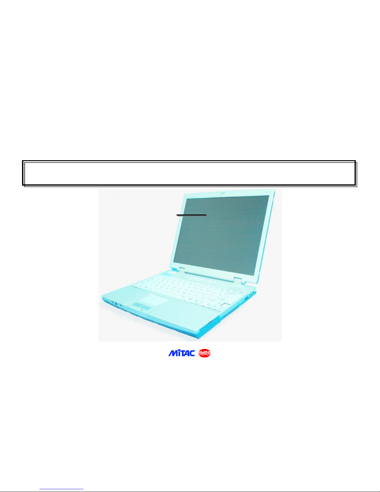
SERVICE MANUAL & TROUBLESHOOTING GUIDE FOR
SERVICE MANUAL & TROUBLESHOOTING GUIDE FOR
SERVICE MANUAL & TROUBLESHOOTING GUIDE FOR
7521
7521
TESTING TECHNOLOGY DEPARTMENT / TSSC
TESTING TECHNOLOGY DEPARTMENT / TSSC
BY
BY
::::
::::
Jesse .Jan
Jesse .Jan
MAR. 2001
MAR. 2001
Page 2

1
7521
7521
N/B MAINTENANCE
N/B MAINTENANCE
1. HARDWARE ENGINEERING SPECIFICATION……………………..
2. DEFINITION & LOCATION CONNECTORS/ SWITCHES…………..
3. DEFINITION & LOCATION MAJOR COMPONENTS………………..
4. PIN DESCRIPTIONS OF MAJOR COMPONENTS ……………………
5. SYSTEM VIEW & DISASSEMBLY ……………………………………….
6. MAINTENANCE DIAGNOSTICS………………….………………………
7. TROUBLE SHOOTING …………………………………….……………..
8. SPARE PARTS LIST ……………………………….………………………
9. BLOCK DIAGRAM ………………………………………………………..
10. EXPLODED DRAWING…………………………………………………..
11. CIRCUIT DIAGRAM……………………………………………………...
P.2
P.40
P.44
P.47
P.60
P.84
P.88
P.120
P.128
P.129
P.130
CONTENTS
Page 3

2
7521
7521
N/B MAINTENANCE
N/B MAINTENANCE
1.1 HARDWARE ENGINEERING SPECIFICATION
1.1.1 General Description
This document describes the engineering specification for 7521 portable notebook computer system.
1.1.2 System Overview
The 7521 model motherboard will accept Intel Pentium III and Celeron processor with FC-PGA packaged. Which will
supports the different levels of Pentium III CPU with FC-PGA package. Those are Pentium III 600/650/700/750/800 MHz,
and Celeron 600/633/667/700/733 MHz .
This system is based on PCI architecture and is fully compatible with IBM PC/AT specification, which have standard
hardware peripheral interface and support Intel Pentium III with FC-PGA package. The power management complies with
Advanced Configuration and Power Interface (ACPI) 1.0. It also provides easy configuration through CMOS setup, which
is built in system BIOS software and can be pop-up by pressing F2 at system start up or warm reset. System also provides
icon LEDs to display system status, such as AC Power indicator, FDD, HDD, NUM LOCK, CAP LOCK, SCROLL LOCK,
SUSPEND MODE and battery present, capacity & charging status. It also equipped with LAN, FIR, USB port, 3D stereo
audio functions.
The memory subsystem supports 64MB on board SDRAM, one 144pin DIMM socket for upgrading up to 192 MB of
DRAM using SDRAM DIMM module.
The SiS 630 integrates the north bridge chip, super south bridge and the real 128-bit 3D graphics accelerator all into one
single chip. It provides 10/100M Fast Ethernet, 3D Positional Audio, Advance H/W DVD playback and 2D/3D graphics
engine.
Page 4

3
7521
7521
N/B MAINTENANCE
N/B MAINTENANCE
The TI 1225 cardbus controller supports PCMCIA and CARDBUS. The National Semiconductor PC97338 Super I/O
controller integrates the standard PC I/O functions: floppy interface, two FIFO serial ports, one EPP/ECP capable
parallel port, and support for an IrDA 1.1, 1.0 and sharp ASK compatible infrared interface. To provide for the
increasing number of multimedia applications, an CODEC CS4299 is integrated onto the motherboard which support
16-bit stereo, Sound Blaster Pro, Windows Sound System compatibility, and full-duplex capabilities to meet the
demands of interactive multimedia applications
A full set of software drivers and utilities are available to allow advanced operating systems such as Windows 95 or
Windows 98 to take full advantage of the hardware capabilities. Features such as bus mastering IDE, Windows 95ready Plug and Play, Advanced Power Management (APM) with application restart, software-controlled power
shutdown..
1.2 Hardware System
1.2.1 System parts
• Central Processing Unite : using Intel Pentium ! or Celeron microprocessors in FC-PGA packaged.
• Synthesizer : ICS9248-102.
• SiS 630 : CPU/ PCI and CPU/AGP bridge with memory controller/LAN/IDE/USB/PMU controller.
• Super I/O Controller : NS PC 97338VJG.
• PCMCIA Interface Controller : TI 1225.
• Keyboard System : Hitachi H8 (3434F) universal keyboard controller.
• 3D Audio System : CRYSTAL CS 4299 CODEC.
• FIR port : HP HSDL-3600#007 FIR module.
• FAX/ MODEM : ASKEY 56Kbps Fax MODEM, software Modem (Option) .
Page 5

4
7521
7521
N/B MAINTENANCE
N/B MAINTENANCE
1.2.2 CPU MODULE
• Intel Pentium !/ Celeron Processors with 370 pins PGA package.
• Pentium ! 600/650/700/750/800 MHz, FC-PGA package at FSB 100MHz.
• Celeron 600/ 633/ 667/ 700/ 733 MHz, FC-PGA package.
1.2.3 Synthesizer
• System frequency synthesizer : ICS9248-102
- Maximized EMI suppression using Integrate Circuit System’s spread spectrum technology.
- Three copies of CPU output, output to output skew between them within 175ps and seven copies of PCI output, output to
output skew between them 500ps, fourteen copies of SDRAM output, output to output skew between them within 250ps.
- One 48MHz outout for USB and selectable 24/48 MHz output ( pin25 ).
- Two buffer copies of 14.318MHz input reference signal.
- Supports up to 166MHz CPU or SDRAM operation.
- Supports two SDRAM DIMMS.
- Ideal for high performance Desktop/ Notebook designed using SIS630 chip set.
- I²C serial configuration interface.
1.2.4 SiS630 Slot 1/Socke t 37 0 2D/3D Ultra-AGP™ Single Chipset
The single chipset SiS630, provide a high performance/ low cost Desktop soloution for the Intel Slot 1 and socket 370 series
CPUs based system by integrated a high performance North Bridge, advanced hardware 2D/3D GUI engine and Super-South
bridge. In addition. SiS630 provides system-on-chip solution that complies with Easy PC Initiative which supports instantly
Available OnNow PC technology, USB, Legacy Removal and Slotless Design and FlexATX form factor.
Page 6

5
7521
7521
N/B MAINTENANCE
N/B MAINTENANCE
By integrating the UltraAGP™ technology and advanced 128-bit graphic display interface, SiS630 delivers AGP 4x-like
performance and up to 2 GB/s memory bandwidth. Furthermore, SiS630 provides powerful hardware decoding DVD
accelerator to improve the DVD playback performance. In addition to providing the standard interface for CRT monitors,
SiS630 also
provides the Digital Flat Panel Port (DFP) for a standard interface between a personal computer and a digital flat panel
monitor. To extend functionality and flexibility, SiS also provides the ?Video Bridge?(SiS301) to support the NTSC/PAL
Video Output, Digital LCD Monitor and Secondary CRT Monitor, which reduces the external Panel Link transmitter and
TV-Out encoder
for cost effected solution. SiS630 also adopts Share System Memory Architecture which can flexibly utilize the frame buffer
size up to 64MB.
The “Super-South Bridge” in SiS630 integrates peripheral controllers / accelerators / interfaces. SiS630 provides a total
communication solution including 10/100Mb Fast Ethernet for Office requirement and 1Mb HomePNA for Home
Networking. SiS630 offers AC’97 compliant interface that comprises digital audio engine with 3D-hardware accelerator, onchip
sample rate converter, and professional wavetable along with separate modem DMA controller. SiS630 also provides
interface to Low Pin Count (LPC) operating at 33 MHz clock which is the same as PCI clock on the host, and dual USB host
controller with five USB ports that deliver better connectivity and 2 x 12Mb bandwidth.
The built-in fast PCI IDE controller supports the ATA PIO/DMA, and the Ultra DMA33/66 function that supports the data
transfer rate up to 66 MB/s. It provides the separate data path for two IDE channels that can eminently improve the
performance under the multi-tasking environment.
Features
Host Interface Controller
Supports Intel Pentium III/Celeron CPU at 100/66MHz Front Side Bus Frequency
Synchronous Host/DRAM Clock Scheme
Asynchronous Host/Dram Clock Scheme
Page 7

6
7521
7521
N/B MAINTENANCE
N/B MAINTENANCE
Integrated DRAM Controller
3-DIMM/6-Bank of 3.3V SDRAM
Supports NEC Virtual Channel Memory (VC-SDRAM) Technology
Supports Memory Bus up to 133MHz
System Memory Size up to 1.5GB
Up to 512 MB per Row
Supports 16Mb, 64Mb, 128Mb, 256Mb, 512Mb, SDRAM Technology
Suspend-to-RAM (STR)
Relocatable System Management Memory Region
Programmable Buffer Strength for CS#, DQM[7:0], WE#, RAS#, CAS#, CKE, MA[14:0] and MD[63:0]
Shadow RAM Size from 640KB to 1MB in 16KB incrementss
Two Programmable PCI Hole Areas
Integrated A.G.P. Compliant Target /66Mhz Host-to-PCI Bridge
AGP v2.0 Compliant
Supports Graphic Window Size from 4MBytes to 256MBytes
Supports Pipelined Process in CPU-to Integrated 3D A.G.P. VGA Access
Supports 8 Way, 16 Entries Page Table Cache for GART to Enhance Integrated A.G.P. VGA Controller Read/Write
Performance
Supports PCI-to-PCI Bridge Function for Memory Write from 33MHz PCI Bus to Integrated A.G.P. VGA
Page 8

7
7521
7521
N/B MAINTENANCE
N/B MAINTENANCE
Meet PC99 Requirements PCI 2.2 Specification Compliant High Performance PCI Arbiter
Supports up o 4 PCI Masters
Rotating Priority Arbitration Scheme
Advanced Arbitration Scheme Minimizing Arbitration Overhead
Guaranteed Minimum Access Time for CPU and PCI Masters
Integrated Host-to-PCI Bridge
Zero Wait State Burst Cycles
CPU-to-PCI Pipeline Access
256B to 4KB PCI Burst Length for PCI Masters
PCI Master Initiated Graphical Texture Write Cycles Re-mapping
Reassembles PCI Burst Data Size into Optimized Block Size
Fast PCI IDE Master/Slave Controller
Supports PCI Bus Mastering
Native Mode and Compatibility Mode
PIO Mode 0,1,2,3,4
Multiword DMA Mode 0,1,2
Ultra DMA 33/66
Two Independent IDE Channels Each with 16 DW FIFO
Page 9

8
7521
7521
N/B MAINTENANCE
N/B MAINTENANCE
Virtual PCI-to-PCI Bridge
Integrated Ultra AGP VGA for Hardware 2D/3D Video/Graphics Accelerators
Supports Tightly Coupled 64 Bits 100mhz Host Interface to VGA to Speed Up GUI Performance and Video Playback
Frame Rate
AGP v. 2.0 Compliant
Zero-Wait-State 128x4 Post-Write Buffer with Write Combine Capability
Zero-Wait-State 128x4 2-Way Read Ahead Cache Capability
Re-locatable Memory-Mapped and I/O Address Decoding
Flexible Design Shared Frame Buffer architecture for Display Memory
Shared System Memory Area up to 64MB
Built-in 8K Bytes Texture Cache
32-Bit VLIW Floating-Point Primitive Setup Engine
Peak Polygon Rate : 4M Polygon/Sec@1 Pixel/Polygon With 16bpp, Bilinear Textured, Z Buffered and Alpha Blended
Supports Flat and Ground Shading
Supports High Quality Dithering
Supports Z-Test, Stencil Test, Alpha Test and Scissors Clipping Test
Supports Z Pre-Test for Reducing texture Read Dram Bandwidth
Supports 256 Rops
Supports Individual Z-Buffer and Render Buffer at the same time
Supports 16/24/32 BPP Z Buffer Integrater/Floating Formats
Page 10

9
7521
7521
N/B MAINTENANCE
N/B MAINTENANCE
Supports 16/32 BPP Render Buffer Foramt
Supports 1/2/4/8 Stencil Format
Supports Per-Pixel Texture/Fog Perspective Correction
Supports MIPMAP with Point-Sampled, Linear, Bi-Linear and Tri-Linear Texture Filtering
Supports Single Pass Two MIPMAP Texture, One Texture on Clock
Supports up to 2048x2048 Texture Size
Supports 2?s Power of Width and height structure rectangular texture
Supports 1/2/4/8 BPP Palletize Texture with 32 Bit ARGB Format
Supports Fogging and Alpha Blending
Supports Hardware Back Face Culling
Supports YUV-to-RGB Color Space Conversion
Supports CD/DVD to TV Playback Mode
Supports DVD Sub-Picture Playback Overlay
Built-in Programmble 24-bits True-Color RAMDAC up to 270 MHz Pixel Clock RAMDAC Snoop Function
Supports VESA Standard Super High Resolution Graphic Modes
- 640x480 16/256/32K/64K/16M colors 120 Hz NI
- 800x600 16/256/32K/64K/16M colors 120 Hz NI
- 1024x768 256/32K/64K/16M colors 120Hz NI
- 1280x1024 256/32K/64K/16M colors 120Hz NI
- 1600x1200 256/32K/64K/16M colors 100Hz NI
- 1920x1200 256/32K/64K/16M colors 80Hz NI
Page 11

10
7521
7521
N/B MAINTENANCE
N/B MAINTENANCE
Cooperate with "iS Video Bridge ?to support
- NTSC/PAL Video Output
- Digital LCD Monitor
- Secondary CRT Monitor
Low Pin Count Interface
Forwards PCI I/O and Memory Cycles into LPC bus
Translates 8/16 bit DMA cycles into PCI bus cycles
Advanced PCI H/W Audio & Modem
Advanced Wavetable Synthesizer
DirectSound™ 3D
Advanced Streaming Architecture
High Quality Audio and AC”97/98 Support
Full Legacy Compatibility
Telephony & Modem
Software support
Meets ACPI 1.0 Requirement
Meets APM 1.2 Requirement
ACPI Sleep States Include S1, S2, S3, S4, S5
CPU Power States Include C0, C1, C2, C3
Power Button with Override
Page 12

11
7521
7521
N/B MAINTENANCE
N/B MAINTENANCE
RTC Day-of-Month, Month-of-Year Alarm
LED Blinking in S0, S1, S2, S3
PCI Bus Power Management Interface Spec. 1.0
Integrated DMA Controller
Two 8237A Compatible DMA Controller
8/16 bit DMA data transfer
Distributed DMA Support
Integrated Interrupt Controller
Two 8237A Compatible DMA Controller
Two 8259A Compatible Interrupt Controllers
Level or Edge Triggered programmable
Serial IRQ
Interrupt Source Re-routable to Any IRQ channel
Three 8254 Compatible Programmable 16-bits counters
System timer interrupt
Generate refresh request
Speaker output
Page 13

12
7521
7521
N/B MAINTENANCE
N/B MAINTENANCE
Integrated Keyboard Controller
Supports PS/2 mouse interface
Password security and password power-up
System sleep and power-up by Hot-Key
KBC and PS2 mouse can be individually disabled
Integrated Real Time Clock (RTC) with 256B CMOS SRAM
Supports ACPI Day-Month and Month-of-Year- Alarm
256 Bytes of CMOS SRAM
Provides RTC H/W Year 2000 Solution
Universal Serial Bus Host Controller
Open HCI Host Controller with Root Hub
Two USB Host Controller
Five USB Ports
Supports Legacy Devices
Over Current Detection
Page 14

13
7521
7521
N/B MAINTENANCE
N/B MAINTENANCE
I²C Bus/SMBus Series Interface
Plug and Play Compatible
High-Performance 32-Bit PCI Bus Master Architecture with Integrated Direct Memory
Access (DMA) Controller for Low CPU and Bus utilization
Supports PCI Device ID, Vendor ID / Subsystem ID , Subsystem Vendor ID
Programming through the EEPROM interface
Implements Optional PCI 3.3v Auxiliary Power Source 3.3Vaux Pin and Optional PCI
IEEE 802.3 and 802.3u Standard Compatible
IEEE 802.3u Auto Negotiation and Parallel Detection for Automatic Speed Selection
Full Duplex and Half Duplex Mode for both 10 and 100 Mbps
Fully Compliant Ansi X3.263 Tp-Pmd Physical Sub-Layer which includes adaptive
Single 25mhz Clock for 10 and 100 Mbps Operation
Power Down of 10 base-T/100base-Tx sections when not in use
Supports 10base-Tx, 100base-Tx
1.2.5 Super IO: NS PC 97338VJG
High speed PC16550A compatible UART with receive/transmit 16 Bytes FIFO programmable serial baud rate generator
Multi-mode parallel port support including standard port, EPP/ECP (IEEE1284 compliant, 2 interrupt pins)
Plug and Play module
FDC, 100% IBM compatible, S/W & register compatible to 82077 with 16Bytes data FIFO Support 3-Mode FDD
FIR/MIR/SIR/SHARP ASK for Infrared application.
COM2
Page 15

14
7521
7521
N/B MAINTENANCE
N/B MAINTENANCE
IrDA 1.0 / IrDA 1.1 / SHARP ASK
- Baud rate: max. 4Mb
- Link distance: 0.01 to 1 m
- Half angle: #15…⌡ .Βιτ∃Error Rate (BER) : 10
-9
- Peak wavelength: 0.85 - 0.90 mm.
TQFP 100 pins
Standby mode: control by software
Default configuration :
IO address IRQx DRQx
COM1 3F8-3FF 4 -
FIR/MIR/SIR/
SHARP ASK 278-27F 3 ( COM2 )
PIO 378-37F 7 -
FDD 3F0-3FF 6 2
Page 16

15
7521
7521
N/B MAINTENANCE
N/B MAINTENANCE
1.2.6 PC CARD interface controller: TI1225
ACPI 1.0 Compliance
PCI Power Management interface specification 1.0 Compliance
Supports distributed DMA (DDMA) and PC/PCI DMA
Advanced submicron, low-power CMOS technology.
Supports two I/O windows and two memory windows available to each cardbus socket.
Supports five PCI memory windows and two I/O windows available to each PC CARD16 socket.
Supports Burst Transfers To Maximize Data Throughput On Both PCI Buses
Provides Serial Interface To TI TPS2202/TPS2206 Dual Slot PC CARD Power Interface Switch
Supports up to 5 general purpose I/O
Multi-Function PCI Device With Separate Configuration Space For Each Socket
Pipelined architecture allows greater than 130Mbps second throughput from cardbus to PCI and from PCI to cardbus.
Support PCI Bus Lock (/LOCK)
3.3-V core logic with universal PCI interface
PCI Local Bus Specification Revision 2.1 compliant
Fully compatible with the Intel 430TX(Mobile Triton II) chipset
1995 PC Card Standard compliant
Supports two 16-bit PC card or Cardbus card; sockets powered at 3.3V or 5V with hot insertion and removal
Provides a serial EEPROM interface for loading the subsystem ID and subsystem vendor ID.
ExCA compatible Registers mapped in memory or I/O space.
Supports ring indicate output, SUSPEND# , and programmable output select for CLKRUN#.
Page 17

16
7521
7521
N/B MAINTENANCE
N/B MAINTENANCE
Provides socket activity LED signals.
Provides zoom video support signals.
Provides zoom video port function in socket B.
208-Pin LQFP package
1.2.7 DUAL-SLOT PC CARD POWER INTERFACE SWITCH: TPS2206
Fully Integrated Vcc and Vpp Switching for Dual-Slot PC Card Interface
P 2 C3-Lead Serial Interface Compatible With CardBus Controllers
3.3 V Low-Voltage Mode
Meets PC Card Standards
RESET for System Initialization of PC Cards
12-V Supply Can Be Disabled Except During 12-V Flash Programming
Short Circuit and Thermal Protection
30-Pin SSOP (DB) and 32-Pin TSSOP (DAP)
Compatible With 3.3-V, 5-V and 12-V PC Cards
Lower DS(on) (140-m .5-V Vcc Switch; 110-m .3.3-V Vcc Switch)
Break-Before-Make Switching
Page 18

17
7521
7521
N/B MAINTENANCE
N/B MAINTENANCE
1.2.8 Keyboard system: H8(3434F) universal keyboard controller
CPU
- Two-way general register configuration
- Eight 16-bit registers or Sixteen 8-bit registers
- High-speed operation
- Maximum clock rate: 16Mhz at 5V
Memory
- Include 32KB ROM and 1KB RAM
16-bit free-running timer
- One 16-bit free-running counter
- Two output-compare lines
- Four input capture lines
8-bit timer (2 channels)
- Each channel has one 8-bit up-counter , two time constant registers
PWM timer (2 channels)
- Resolution: 1/250
- Duty cycle can be set from 0 to 100%
I²C bus interface (one channel)
- Include single master mode and slave mode
Host interface (HIF)
- 8-bit host interface port
- Three host interrupt requests ( HIRQ1,11,12)
- Regular and fast A20 gate output
Page 19

18
7521
7521
N/B MAINTENANCE
N/B MAINTENANCE
Keyboard controller
- Controls a matrix-scan keyboard by providing a keyboard scan function with wake-up
- Interrupts and sense ports
A/D converter
- 10-bit resolution
- 8 channels : single or scan mode (selectable )
D/A converter
- 8-bit resolution
- 2 channels
Interrupts
- nine external interrupt lines : NMI# , IRQ0 to 7#
- 26 on-chip interrupt sources
Power-down modes
- Sleep mode
- Software standby mode
- Hardware standby mode
A single chip microcomputer
On-chip flash memory
Maximum 64-kbyte address space
Support three PS/2 port for external keyboard ,mouse and internal track pad.
Support SMI,SCI trigger input:
Cover switch
Page 20

19
7521
7521
N/B MAINTENANCE
N/B MAINTENANCE
Battery charging control
Smart Battery monitoring
Control D/D system on/off
Fan control and LED indicator serial interface
100pin TQFP
1.2.9 Memory System
1.2.9.1 Main Memory
HYUNDAI : GM72V281641AT-7K SDRAM
NEC : UPD45128163G5-A80-9JF SDRAM
- one chip memory size: 4Banksx1Mx16bit SDRAM.
- Standard 54 pin TSOP-II package.
- Power supply: 3 $0.3V
Supports One JEDEC 144-pin S.O. DIMM sockets on Mother Board for expansion
Supports 3.3V SDRAM
2 banks on one socket.
SDRAM accesses time from clock: 6ns
Memory bus bandwidth: 64 bits
Page 21

20
7521
7521
N/B MAINTENANCE
N/B MAINTENANCE
7521 Supports 64 MB SDRAM on board and one 144pin DIMM socket for upgrading up to 320MB of DRAM .
Here are some main memory system essential characteristics:
- One chip 4Banksx1Mx16bit on board 64 MB
- 144-pin S.O. DIMM socket 1
- Memory Voltage 3.3V $ 10%
- Banks on DIMM Total:2
- Mixed type DRAM Only supports SDRAM
1.2.10 Interface
Power Supply Jack.
One Standard Parallel Port With ECP/EPP Functions
Supports Two USB port for all USB device.
Supports Macrovision’s TV-OUT connector.(layout only)
Tunable volume by variable resistor .
Two Serial Ports, One For COM1/COM2, The Other For FIR/MIR/SIR/SHARP ASK
One External CRT Connector For CRT Display
One PS/2 Interface For External KB, Mouse Or Other Devices
Two Cardbus Sockets
Cable For Connection Between M/B And Panel.
Cable For Connection Between M/B And Backlight BD.
Headphone Out Jack, Microphone Input Jack And Line In Jack.
One MODEM RJ-11 phone jack for PSTN line and RJ-45 for LAN.
Page 22

21
7521
7521
N/B MAINTENANCE
N/B MAINTENANCE
Battery translation board connection between M/B and battery.
Quick start buttons translation board (QSB) connection between M/B and five Buttons.
Internet quick start button translation board (IQSB) connection between M/B and touch pad, five LEDs, two Buttons.
FDD-HDD translation board connection between M/B and floppy, hard disk.
One CD-ROM connector on M/B.
1.2.11 Audio System: AC’97 CODEC CS4299
AC’97 CODEC CS4299 provides a complete high quality audio solution, Feature Include:
- MPU-401 interface
- FM synthesizer
-Game Port
- MIDI port.
- MODEM
- CD-ROM
- User-Defined GPIO
- Volume Control: Rotary VR
Stereo BTL 2x1 W Amplifiers(TPA0202) With 8 Ohm Load.
CD-ROM IDE Interface
18-bit Stereo ADC & 20-bit Stereo DAC For Record And Play Back
Programmable Sample Rates From 20Hz To 20kHz For Record And Playback
Microphone in * 1 (3.5 mm phone-jack)
Headphone out * 1: stereo (3.5 mm phone-jack and SCMS support)
Page 23

22
7521
7521
N/B MAINTENANCE
N/B MAINTENANCE
Line in * 1(3.5 mm phone-jack)
Built-in Speaker * 2 (1w, 8 ohm)
Built-in Microphone * 1
Note: For Those Input Source Not Using Should Be Set Mute In Order To Reduce Noise. Like Line In
1.2.12 IR MODULE: HSDL-3600#007
Fully Compliant to IrDA 1.1 Specifications
- 115.2 kb/s to 4 Mb/s operation
- excellent nose-to-nose operation
Compatible with ASK, HP-SIR, and TV Remote
IEC825-Class 1 Eye Safe
Wide Operating Voltage Range
- 2.7 V to 5.25 V
Small Module Size
- 4.0 x 12.2 x 5.1 mm (HxWxD)
Complete Shutdown
- TXD, RXD, PIN diode
Low Shutdown Current
- 10 nA typical
Adjustable Optical Power Management
- Adjustable LED drive-current to maintain link integrity
Page 24

23
7521
7521
N/B MAINTENANCE
N/B MAINTENANCE
Single Rx Data Output
- FIR Select pin switch to FIR
Integrated EMI Shield
- Excellent noise immunity
Edge Detection Input
- Prevents the LED from long turn-on time
Interface to various Super I/O and Controller Devices
Designed to Accommodate Light Loss with Cosmetic Window
Minimum External Components Required
Page 25

24
7521
7521
N/B MAINTENANCE
N/B MAINTENANCE
1.2.13 Special Feature Function
1.2.13.1 Hot Key Function
Keys Combination Feature Meaning
Fn + F5 LCD/external CRT Rotate display mode in LCD only, CRT only and
switching simultaneously display.
Fn + F6 Brightness down Decreases the LCD brightness / No function in
DSTN model
Fn + F7 Brightness up Increases the LCD brightness / No function in
DSTN model
Fn + F10 Enable/Disable Battery Toggle Battery Warning on/off
Warning Beep
Fn + F11 Panel Off/On Toggle Panel Off/On
Fn + F12 Suspend to DRAM/HDD Force the computer into either Suspend to HDD or
Suspend to DRAM mode depending on BIOS
Setup.
Page 26

25
7521
7521
N/B MAINTENANCE
N/B MAINTENANCE
1.2.13.2 Quick Start Button function
Keys Feature Meaning
IQSB
Mail Received Button (or
function “Recognizable
Signal”)
Determined by Software component.
ESB1 Entertainment Quick Key Determined by Software component.
ESB2 Instant Interne t Determined by Software component.
ESB3 My Presario Determined by Software component.
ESB4 Search
Determined by Software component.
ESB5 Email
Determined by Software component.
Page 27

26
7521
7521
N/B MAINTENANCE
N/B MAINTENANCE
1.2.13.3 Flash ROM (BIOS)
7521 system utilizes the state-of-the-art Flash EEPROM technology. User can upgrade the system BIOS in the future just
running the program from MiTAC.
1.2.13.4 LED Indicators
System has ten status LED indicators to display system activity which include above keyboard and below touch pad:
1. Four LED indicators below touch pad:
From left to right that indicates MAIL RECEIVED, AC POWER, BATTERY POWER and BATTERY STATUS:
Mail Received status: This LED lights to indicate that User received E-mail status. User can define color of LED (yellow
or green) to indicate relation of transmitter.
AC POWER: This LED lights green when the notebook is being powered by AC, and flash (on 1 second, off 1 second )
when Suspend to DRAM is active using AC power. The LED is off when the notebook is off or powered by batteries,
or when Suspend to Disk.
BATTERY POWER: This LED lights green when the notebook is being powered by batteries, and flashes (on 1
second, off 1 second ) when Suspend to DRAM is active using battery power. The LED is off when the notebook is off
or powered by AC, or when Suspend to Disk.
BATTERY STATUS : During normal operation, this LED stays off as long as the battery is charged. When the battery
charge drops to 10% of capacity, the LED lights red, flashes per 1 second and beeps per 2 second. When AC is
connected, this indicator glows green if the battery pack is fully charged, or orange (amber) if the battery is being
charged.
2. Six LED indicators above keyboard:
From left to right that indicates CD-ROM/MO, HARD DISK DRIVE, FLOPPY DISK DRIVE, NUM LOCK, CAPS
LOCK and SCROLL LOCK.
Page 28

27
7521
7521
N/B MAINTENANCE
N/B MAINTENANCE
1.2.13.5 COM port assignment
COM1: MODEM / RS-232 / Disable
COM2: IR / RS-232 / Disable
1.3 SMM and System BIOS
1.3.1 System Manage ment Mode
7521 system has built in several power saving modes to prolong the battery usage for mobile purpose. User can enable and
configure different degrees of power management modes via ROM CMOS setup (booting by pressing F2 key). Following are
the descriptions of the SMM and power management modes supported.
1.3.1.1 Full On Mode
In this mode, each device is running with the maximal speed. CPU clock is up to its maximum.
1.3.1.2 Doze Mode
In this mode, CPU will be toggling between on & stop grant mode either. The technology is clock throttling. This can save
battery power without loosing much computing capability. The CPU power consumption and temperature is lowered in this
mode.
1.3.1.3 Standby Mode
For more power saving, it turns of f the peripheral component. In this mode, the following is the status of each device.
CPU: Stop grant
LCD: backlight off
HDD: spin down
FDD: standby
Page 29

28
7521
7521
N/B MAINTENANCE
N/B MAINTENANCE
1.3.1.4 Suspend Mode
The most chipset of the system is entering power down mode for more power saving. In this mode , the following is the
status of each device.
1.3.1.4.1 Suspend to DRAM:
CPU: off
SiS630: Partial off
VGA: off
PCMCIA: off
Super IO: off
Audio: off
SDRAM: Self Refresh.
1.3.1.4.2 Suspend to HDD:
All devices are stopped clock and power-down,
System status is saved in HDD.
All system status will be restored when powered on again.
Page 30

29
7521
7521
N/B MAINTENANCE
N/B MAINTENANCE
1.3.1.5 Other power management functions
1.3.1.5.1 HDD & Video access
System has the ability to monitor video and hard disk activity. User can enable monitoring function for video and/or hard disk
individually. When there is no video and/or hard disk activity, system will enter next PMU state depending on the application.
When the VGA activity monitoring is enabled, the performance of the system will have some impact.
1.3.1.5.2 Battery Warning
System also provides Battery capacity monitoring and gives user a warning so that users have chance to save his data before
battery dead. Also, this function protects system from mal-function while battery capacity is low.
-Battery Warning: Capacity below 10%, Battery Capacity LED flashes per second, system beeps per 2 seconds. (System beeps
only if BIOS setup enable Battery Warning Beeping. ) System will Suspend to HDD after 2 Minute if BIOS setup enable this
function or system will runs until battery dead without any protection.
1.3.1.5.3 Cover Switch
System automatically provides power saving on monitoring Cover Switch. It will save battery power and prolong the usage
time when user closes the notebook cover unintentionally but the system still in power on mode. There are two functions to be
chosen.
1. Switch to CRT
2. Panel Off
3. Suspend to DRAM or Suspend to Disk by CMOS setup
1.3.1.5.4 Battery Warning State
RedSea system provides battery management function and gives warning while battery is in Its low power state. When the
battery capacity is below 10% (Battery Warning State), system will generate beep for every 2 seconds. When hearing the
beeping, it is recommended that user should plug in AC adapter to get power from external source, or stop working and save
his data file to prevent disaster results.
Page 31

30
7521
7521
N/B MAINTENANCE
N/B MAINTENANCE
1.3.1.5.5 Battery Low State
After Battery Warning State, and battery capacity is below 4%, system will generate beep for twice second.
1.3.1.5.6 Battery Dead State
When the battery voltage level reaches 9 volts, system will shut down automatically in order to extend the battery packs' life.
1.3.2 System BIOS
1.3.3 Fan power on/off management
FAN is controlled by H8 embedded controller which using LM45 to sense CPU temperature and PWM to control fan speed.
1.4 Power Supply System
Please refer to the document for 7521 adapter, DC-to-DC and backlight BD.
1.5 Peripheral Components
1.5.1 LCD PANEL
Hyundai 14X13
- 1024X768 XGA TFT Panel
- Display size (diagonal): 14.1 inch
- 262,144 colors display
- 1 channel LVDS Interface (Flat Link, Ti)
- Display Mode: Normal White
Page 32

31
7521
7521
N/B MAINTENANCE
N/B MAINTENANCE
- Back-light unit : CCFL, 1 tube
- DC for Panel : 3.3V+-0.3V
- Pixel pitch : 0.279(H)X0.279(V)
- Power supply current : 320 mA (Typ)
- Lamp start Voltage : 1500Vrms (25 %)
1.5.2 HDD
FUJITSU MHK2120AT : 12 GB Capacity
— 12.0GB Capacity
— Number of head : 3
— Number of cylinders : 14,784
— Bytes per sector : 512
— Recording method : 16/17 MTR
— Track density : 24,300 TPI
— Bit Density : 383 Kbpi
— Rotational Speed : 4,200 rpm +-1%
— Average Latency : 7.14 ms
— Interface : ATA-5 (Max. Cable length : 0.46 m)
— Data transfer rate :
— To/From Media : 12.5 to 22.3 MB/s
— To/From Host : 66.6 MB/s Max (Ultra-DMA mode 4)
— Data Buffer Size : 512 KB
— Spin up current : 0.9A
rms
— Max. Power Consumption : 4.5W (During spin up)
— Physical Dimensions (H X W X D) : 9.5 mm X 100.0 mm X 70.0 mm
— 15GB, 20GB, 24GB HDD To Be Defined.
Page 33

32
7521
7521
N/B MAINTENANCE
N/B MAINTENANCE
1.5.3 Keyboard
External keyboard: Supports IBM 106 key compatible keyboard
- Key pitch : 19 mm
- Windows95 applied
Internal keyboard: Compatible Japanese keyboard layout (90 keys)
1.5.4 Floppy Disk Drive
Mitsumi D353G
Using High density ( 2HD ) 3.5 inch disk
Data transfer rate: 500k bits/sec
Disk rotational speed: 300 rpm for 2mode, 360rpm for 3mode
Track density: 135 tpi
Track to Track time: 3msec
Page 34

33
7521
7521
N/B MAINTENANCE
N/B MAINTENANCE
1.5.5 Touch Pad
Logic Tech : 904255-0002
Vcc : 5V +- 0.5
Icc(max) : 15 mA
Interface : PS/2
X/Y position resolution : 480+-50 CPI
Dimension : 66mm x 50mm x 5.0mm
effective area : 55mm x 39 mm
Operating Temp. : 0 - 50 degree C
Storage Humidity : 5 - 90 %,
Storage Temp. : -20 - + 60 degree C
ESD : 15KV applied to front surface
1.5.6 24X CD-ROM Drive
System has optional MATSUSHITA UJDA150 24X speed CD-ROM drive, LGS CRN8241B 24X speed CD-ROM drive, or
TEAC CD-224E-A92 24X speed CD-ROM drive.
Hardware interface is compliant with ATAPI IDE specification.
IDE second channel (170h). The default drive is D. User should install the CD-ROM device driver in order to operate this
device. This CD-ROM drive also support audio interface. Co-operate with audio circuit, CD-ROM drive can work as a CD
player.
Ejection: Manual eject using the eject button/Automatically eject using the tray
Page 35

34
7521
7521
N/B MAINTENANCE
N/B MAINTENANCE
XM-1802B:
- average data transfer rate of 3,600 KB/s
- average random seek time of 100ms
- Random access time of 110ms.
- Small size (only 12.7(H) x 128(W) x 129(D)mm)
- Extremely low weight of 230g
- Low average power consumption of 2.4W (maximum only 3.2W).
1.5.7 DVD-ROM drive
MATSUSHITA: UJDA520L-SH 4X speed
- Fast 170 ms Random Access Time (DVD)
- Max. 4X (DVD)/Max. 24X (CD)
- Max. 5,408 Kbytes/s (DVD)/Max. 3,600 Kbytes/s (CD) Sustained Transfer Rate.
- PIO mode-4 ATAPI Drive (16.7 Mbyte/s)
- DMA: Multi word DMA transfer mode-2 (Transfer Rate 16.7 Mbyte/s)
: Ultra DMA mode-2 (Transfer Rate 33.3 Mbyte/s)
Page 36

35
7521
7521
N/B MAINTENANCE
N/B MAINTENANCE
1.5.8 CD-R/RW drive
MATSUSHITA: UJDA310
- WRITE 4X-Speed
- READ max 20X-Speed (CD-RW max 14X-Speed)
- PIOMODE: 16.6MB/s ; Mode 4
- DMAMODE: 4.2MB/s ; Mode 0
- Write: 150KB/s (Normal speed), 300KB/s(2X speed), 600KB/s(4X speed)
- Buffer memory: 2MB
- Access speed 150ms (Typ.)
1.5.9 LED Indicators
Lower ICON LEDs on M/B
- Mail Received status (left 1)
- AC POWER(Left 2)
- BATTERY POWER(right 2)
- BATTERY STATUS(right 1)
Upper ICON LEDs on M/B
- CD-ROM/MO(left 1)
- HARD DISK DRIVE(left 2)
- FLOPPY DISK DRIVE(left 3)
- NUM LOCK(right 3)
-CAPS LOCK(right 2)
- SCROLL LOCK(right 1)
Page 37

36
7521
7521
N/B MAINTENANCE
N/B MAINTENANCE
1.5.10 IR port
HP HSDL-3600#007 FIR Module
- Meet IrDA Physical Layer Specification
- 1 cm to 1 Meter Operating Distance
- 30 degree Viewing Angle
- Support Two Channels - 2.4 Kb/s to 115.2Kb/s and 1.15Mb/s to 4.0 Mb/s
1.5.11 CMOS Battery
CR2032 3V 220mAh lithium battery
When AC in or system main battery in , CMOS battery will no power consumption.
AC or main battery not exist, CMOS battery life at less (220mAh/5.8uA) 4 years.
In normal condition, battery life is at less over 4 years. Battery was put in battery holder, can be replaced
1.5.12 Serial Interface
Using AD ADM3311ARU chip
ESD rating:$3KV
Lead TEMP.(Soldering 10sec):+300 %
Number of RS-232 drivers : 3
Number of RS-232 receivers : 5
28 pin SSOP package
Support shutdown mode(pin 23).
-40 % - +85 % Operating voltage range : 3V $0.3V
MAX. data rate:460 kbps
Shutdown supply current : 15(TYP)uA- 50(MAX)Ua
Page 38

37
7521
7521
N/B MAINTENANCE
N/B MAINTENANCE
1.5.13 PCMCIA socket
Operating temperature range : -55 %- +85 %
Insertion force : 39.2N (MAX)
10000 times insertion and withdrawal at the cycle rate 400- 600cycles/hour and no
evidence of breakage and cracks on the component.
In +85 % 250h life test conditions should be no evidence of breakage and
Cracks on the component.
In -55 % 96h life test conditions should be no evidence of breakage and
Cracks on the component.
1.5.14 FAN
Dimension : Made by Sunonwealth Electric Machine Industry Co. Ltd.
Model number : KD0502PEB2-8 DC brushless fan
Operating speed: 8000 rpm.
Input voltage : 5V
Operating temperature : -10 - +70 degree C.
Weight : 7g
Direction of rotation : C.C.W.
Noise level : 27 dB(A)
Rated power : 0.6 W
Static pressure : 0.09 inch-H2O
Air delivery : 2.3 CFM
Page 39
38
7521
7521
N/B MAINTENANCE
N/B MAINTENANCE
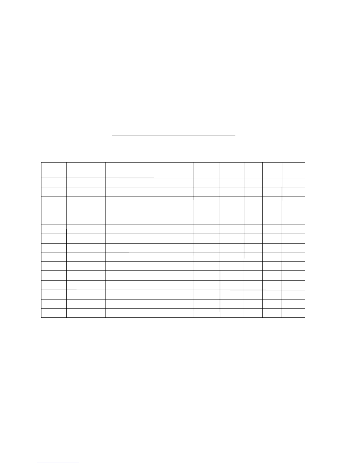
1.6 Appendix 1: GPIO definitions
GPI DEFINITIONS
Signal Function Description During After S1 S3 S4/S5 Remark
Name PCIRST# PCIRST#
GPIO[0] OC0# USB OVER CURRENT High High High Off Off
GPIO[2] RST_CDROM Reset CD-ROM drive High High High Off Off
GPIO[3] EEDO FOR LAN In In Defined Off Off
GPIO[4] KBD_US/JP# In In Defined Off Off
GPIO[5] GPIO5 In In Defined Off Off
GPIO[6] EXTSMI# In In Defined Off Off
GPIO[7] SPDIF SPDIF enable In In Defined Off Off
GPIO[8] GPIO8 In In Defined Off Off
GPIO[9] GND In In Defined Off Off
GPIO[10] FDD_MODE In In Defined Off Off
GPIO[11] SPK_OFF In In Defined Off Off
GPIO[12] RS232_OFF# In In Defined Off Off
GPIO[13] CARD_IN# In In Defined Off Off
GPIO[14] CRT_IN# In In Defined Off Off
GPIO[15] CARD_ACT In In Defined Off Off
Page 40
39
7521
7521
N/B MAINTENANCE
N/B MAINTENANCE
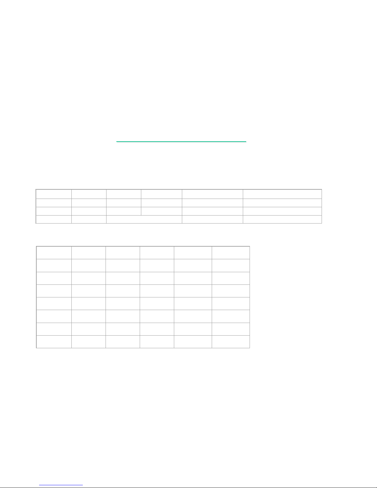
Note 1. LCD ID
LCD_ID2
LCD_ID1 LCD_ID0 Vendor PANEL
1 1 1 HUYNDAI 14X13
Description
Note 3. CPU & SDRAM Frequency setti ng table:
SW_FS3
SW_FS2 SW_FS1 SW_FS0 CPU SDRAM
0 0 0 0 66 100
0 0 0 1 100 100
0 0 1 1 133 100
0 1 0 0 66 133
0 1 0 1 100 133
0 1 1 1 133 133
1 0 0 0 66 66
1.6 Appendix 2: GPIO definitions
GPI DEFINITIONS
Page 41
40
7521
7521
N/B MAINTENANCE
N/B MAINTENANCE
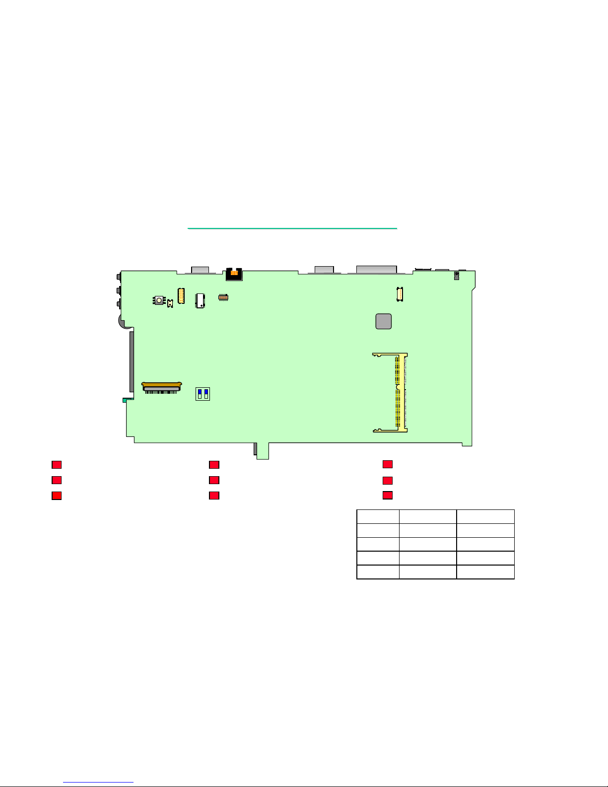
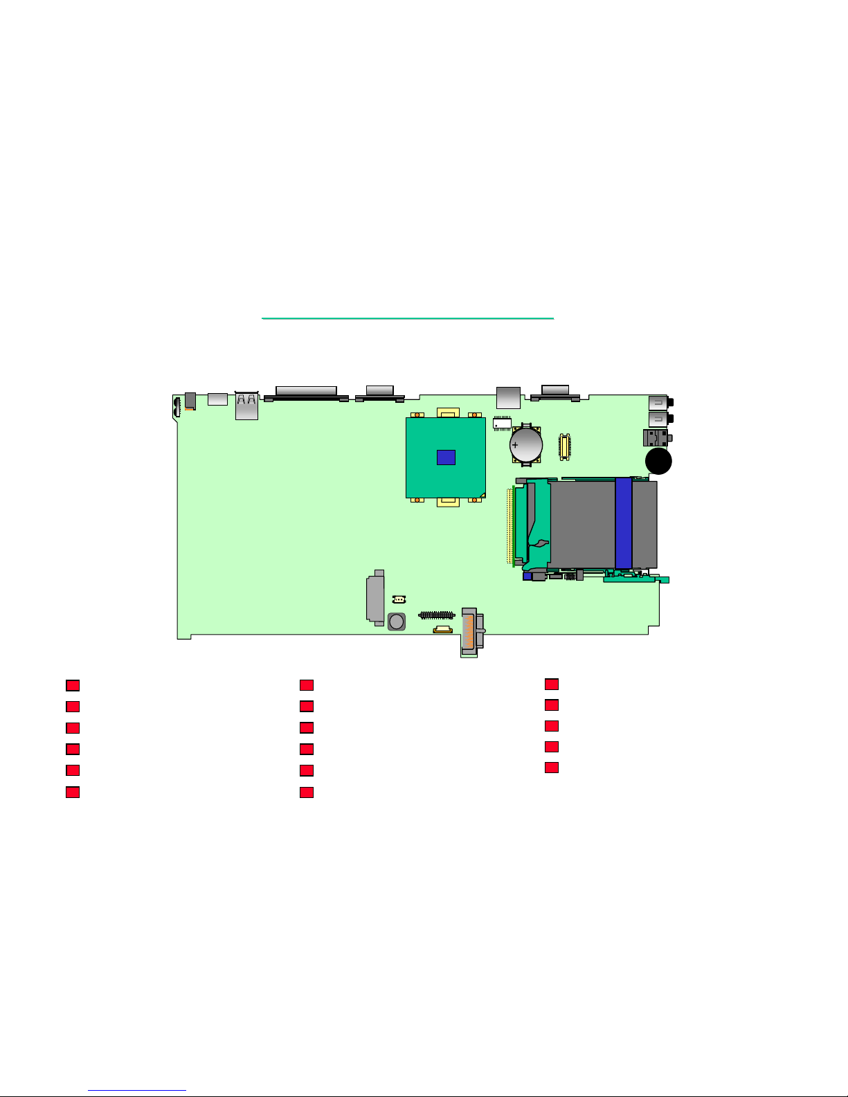
2. DEFINITION & LOCATION OF CONNECTORS/SWITCHES
2.1 Mother Board-A
J1:Inverter BD CONN.
J2: LCD panel connector.
J3: Quick key transfer BD connector.
SW1: Cover Suspend SW.
SW2: Power button.
J4: External MIC-in connector.
J5: Internal keyboard connector.
J6: 144 pins expansion SDRAM socket.
J2
J3
J4
SW2
U2
J5
J6
J1
SW1
OFF
ON
1 2
DIP SW
DIP SW : CPU FSB SELECT
ON
OFF
ON
OFF
DIP SW /BIT2
ON
ON
OFF
OFF
DIP SW /BIT1
100MHZ
150MHZ
66MHZ
133MHZ
FSB
Page 42
41
7521
7521
N/B MAINTENANCE
N/B MAINTENANCE
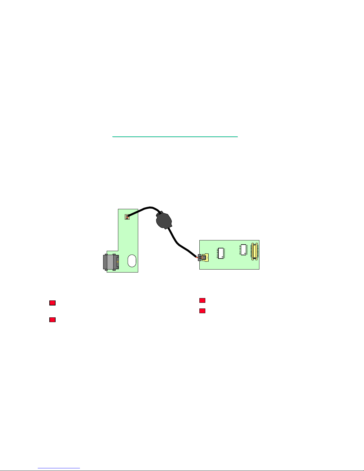
2. DEFINITION & LOCATION OF CONNECTORS/SWITCHES
2.2 Mother Board-B
PJ501: Power jack ( AC adapter).
J502 :PS2 Mouse/keyboard
J503:Line in Jack.
J504: LAN connect
J505:Parallel Port
J507: VGA Connector.
J513: CD-ROM drive connector.
J514:Charger & Touch-Pad connector
J515:Touch-Pad button connector.
BT501: CMOS Battery connector.
VR501: Volume control VR.
U501
PJ501
J502
J508
J505 J507
J504
J506
J503
J509
J510
VR501
U507
J516
J513
J512
J514
J515
BT501
J511
U502
U503
J508: USB connector.
U507: PC card socket.
U503:CPU & CPU Socket.
J511: MODEM transfer board connector
J512: FAN Connector.
J516 :HDD/FDD Connector.
Page 43
42
7521
7521
N/B MAINTENANCE
N/B MAINTENANCE
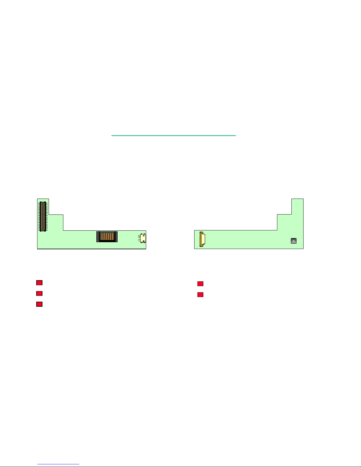
2. DEFINITION & LOCATION OF CONNECTORS/SWITCHES
MDC/LAN transfer board
JP1: MDC jump wire connector.
JP3: Connector 2 for connected
MDC/LAN transfer board
to M/B.
J1: RJ-11 phone jack for internal
modem.
J23: MDC jump wire connector.
2.3 Daughter Board
J1
J23
JP1
U2
U1
JP3
Page 44
43
7521
7521
N/B MAINTENANCE
N/B MAINTENANCE
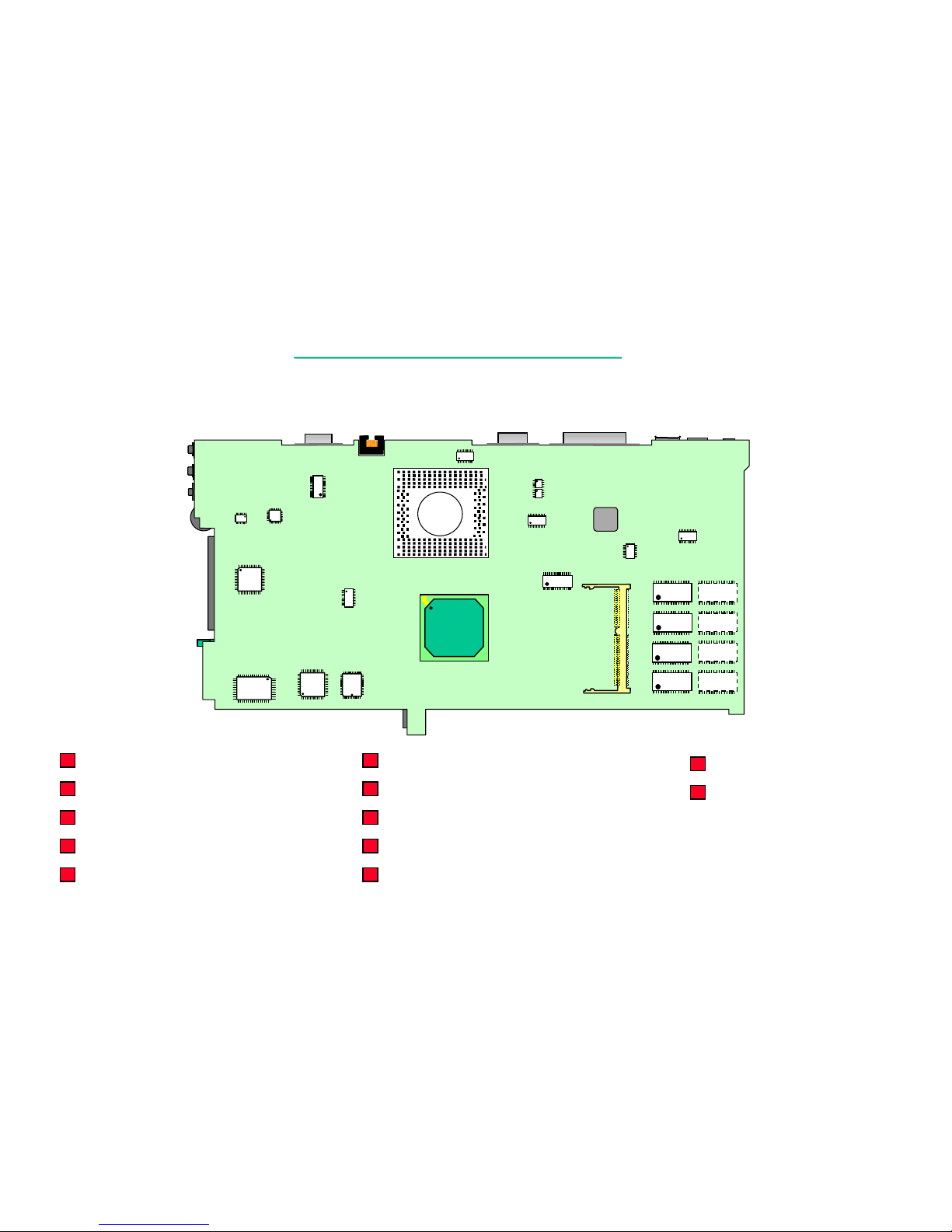
2. DEFINITION & LOCATION OF CONNECTORS/SWITCHES
2.4 Charger Board
Charge board(side B)
J500: Touch-Pad button connector.
SW500: CMOS Reset
Charge board(side A)
J1
PJ4
J2
J500
SW500
J1:Charger & Touch-Pad connector to M/B.
PJ4:Battery pack connector.
J2: Internal speaker connector.
Page 45
44
7521
7521
N/B MAINTENANCE
N/B MAINTENANCE
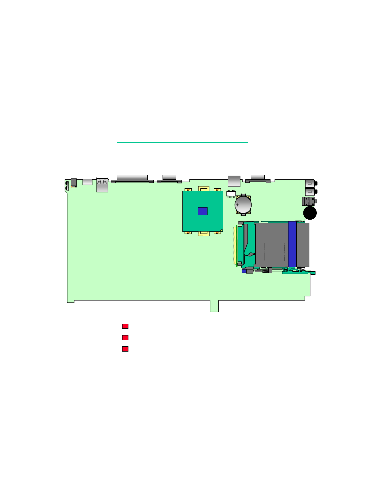
3. DEFINITION & LOCATION OF MAJOR COMPONENTS
3.1 Main Board ( Side A )
U1: ADM3311ARU RS232/SIO.
U2: DS90C363MTD VGA LVD controller.
U5: CS4299 AC’97 CODE.
U6: TPA0202 AUDIO AMP.
U12: H8(3434F) universal.
U6
U12
U2
U17
U31
U27
U28
U22
U13
U15
U20
U25
U29
U16
U21
U26
U30
U1
U5
U31:W83626 LPC to ISA.
U15,U20,U25,U29
: On board SDAM.
U13: ICS9248-102 Frequency Synthesizer.
U17: TPS2206 PCcard Power switch matrix.
U22: SiS630 single chipset.
U27: Super IO PC97338VJG.
U28: System BIOS.
Page 46
45
7521
7521
N/B MAINTENANCE
N/B MAINTENANCE
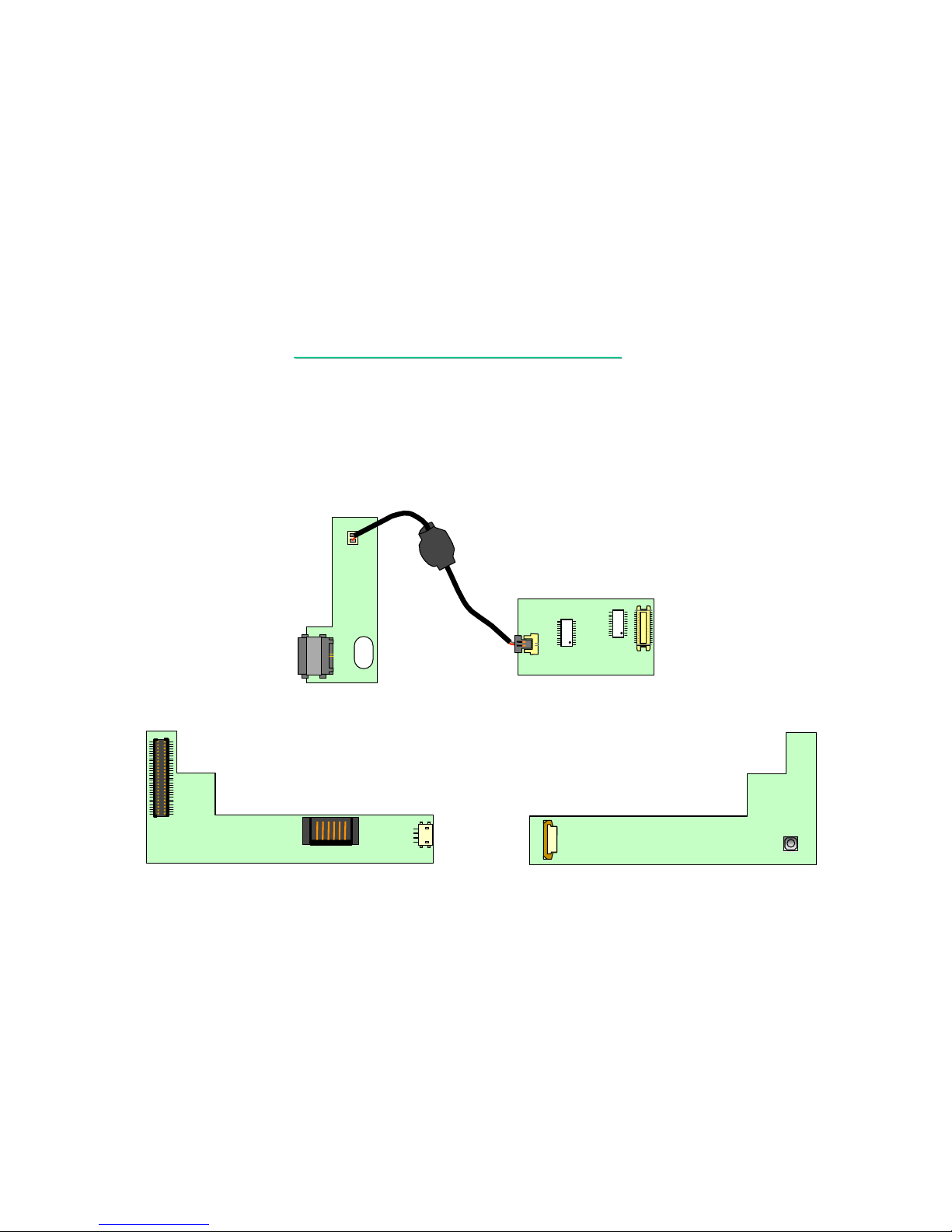
3. DEFINITION & LOCATION OF MAJOR COMPONENTS
3.2 Main Board ( SIDE B )
U502: PH163112 LAN Controller.
U503: Socket 370 CPU.
U505: PCI1225PDV PC CARD interface controller.
U505
U502
U503
Page 47
46
7521
7521
N/B MAINTENANCE
N/B MAINTENANCE
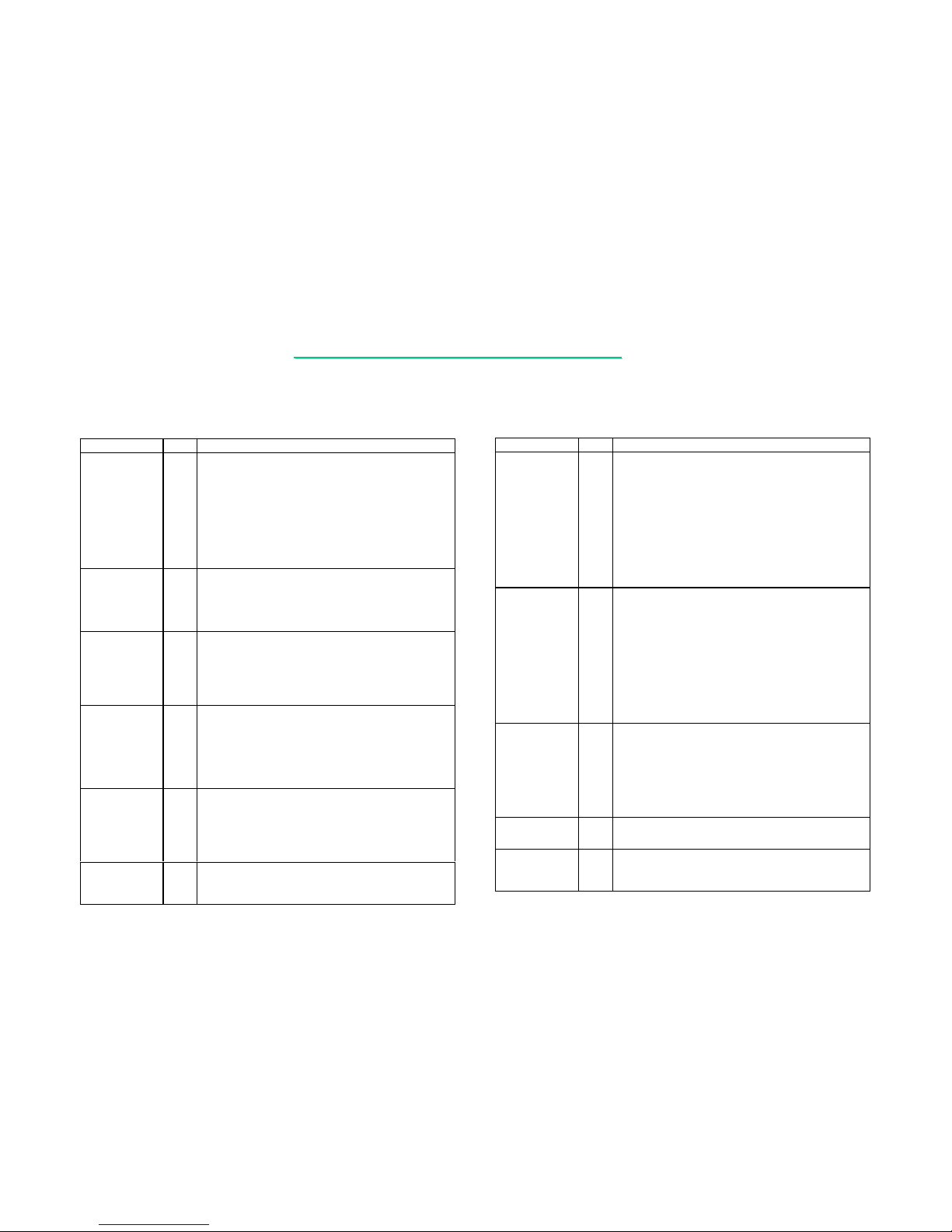
3.3 Definition Of Daughter Board
Charger board (side B) Charger board (side A)
MDC/LAN transfer board
3. DEFINITION & LOCATION OF MAJOR COMPONENTS
J1
J23
JP1
U2
U1
JP3
J500
SW500
J1
PJ4
J2
Page 48
47
7521
7521
N/B MAINTENANCE
N/B MAINTENANCE
4. PIN DESCRIPTIONS OF MAJOR COMPONENTS
4.1 Pentium III/Celeron FC-PGA2 CPU
Alphabetical Signal Reference
Signal Name I/O Signal Description
A[35:3]#
I/O
GTL+
The A[35:3]# (Address) sign als define a 2
36
-byte physical memory
address space. When ADS# is active, these signals transmit the
address of a transaction; when ADS# is inactive, these signals
transmit transaction information. These signals must be connected to
the appropriat e pins/balls of both agents on the system bus. The
A[35:24]# signals are protected with the AP1# parity signal,
and the A[23:3]# signals are protected with the AP0# parity signal.
On the active-to-inactive transition of RESET#, each processor bus
agent samples A[35:3]# signals to determine its power-on
configuration. See Section 4 of this document and the PentiumII
Processor Developer’s Manual for details.
A20M#
I
1.5V
Tolerant
If the A20M# (Address-20 Mask) input signal is asserted, the
processor masks physical address bit 20 (A20#) before looking up a
line in any internal cache and before driving a read/write transaction
on the bus. Asserting A20M# emulates the 8086 processor's address
wrap-around at the 1-Mbyt e boundary. Assertion of A20M# is only
supported in Real mode.
ADS#
I/O
GTL+
The ADS# (Address Strobe) signal is asserted to indicate the validity
of a transaction address on the A[35 :3]# signals. Both bus agents
observe the ADS# activation to begin parity checking, protocol
checking, address decode, internal snoop or deferred reply ID match
operations associated with the new transaction. This signal must be
connected to the appropriate pins/balls on both agents on the system
bus.
AERR#
I/O
GTL+
The AERR# (Address Parity Error) signal is observed and driven by
both system bus agents, and if used, must be connected to the
appropriate pins/balls of both ag ents on the system bus. A ERR#
observation is optionally enabled durin g p ow er - o n co nf iguration; if
enabled, a valid assert ion of AERR# aborts the cur r en t tr an s action.
If AERR# observatio n is disabled during power- o n configuration, a
central agent may handle an assertion of AERR# as appropriate to the
error handling architecture of the system.
AP[1:0]#
I/O
GTL+
The AP[1:0]# (Address Parity) signals are driven by the request
initiator along with ADS#, A[35:3]#, REQ[4:0]# and RP#. AP1#
covers A[35:24]#. AP0# covers A[23:3]#. A correct parity signal is
high if an even number of cover e d s ign a ls ar e low an d l ow if an od d
number of covered signals are low. This allows parity to be high when
all the covered signals are high. AP[1:0]# should be connecte d to the
appropriate pins/balls on both agents on the system bus.
BCLK
I
2.5V
Tolerant
The BCLK (Bus Clock) sig nal determines the system bus frequency.
Both system bus agents must receive this signal to drive their outputs
and latch their inputs on the BCLK rising edge . All external timing
parameters are specified with respect to the BCLK signal.
Signal Name I/O Signal Description
BERR# I/O
GTL+
The BERR# (Bus Error) signal is asserted to indicate an
unrecoverable error without a bus protocol vi olation. It may be driven
by either system bus agent and must be connected to the appropriate
pins/balls of both agents, if used. However, the mobile Pentium III
processors do not observe assertions of the BERR # signal.
BERR# assertion conditions are defined by the system configuration.
Configuration options enable the BERR# driver as follows:
• Enabled or disabled
• Asserted optionally for in ternal errors along with IERR#
• Asserted optionally by the request initiator of a bus transaction after
it observes an erro r
• Asserted by any bus agent when it obser ves an error in a bus
transaction
BINIT# I/O-
GTL+
The BINIT# (Bus Initialization) signal may be observed and driven
by both system bus agents and must be connected to the appropriate
pins/balls of bo th agents, if used. If the BINIT# driver is enabled
during the power-on configuration, BINIT# is asserted to signal any
bus condition that prevents reliable future information.
If BINIT# is enabled during power-on configuration, and BINIT# is
sampled asserted, all bus state machines are reset and any data which
was in transit is lost. All agents reset their rot ating ID for bus
arbitration to the state after reset, and internal count information is
lost. The L1 and L2 caches are not affected.
If BINIT# is disabled during power-on configuration, a central agent
may handle an assertion of BINIT# as appropriate to the Machine
Check Architecture (MCA) of the system.
BNR# I/O-
GTL+
The BNR# (Block Next Request) signal is used to assert a bus stall by
any bus agent that is unable to accept new bus transactions. During a
bus stall, the current bus owner cannot issue any new transactions.
Since multiple agents may need to request a bus stall simultaneously,
BNR# is a wired-OR signal that must be connected to the appropriate
pins/balls of both agents on the system bus. In order to avoid wire-OR
glitches associated with simultaneous edge transitions driven b y
multiple drivers, BNR# is activated on specific clock edges and
sampled on specifi c clock edges.
BP[3:2]# I/O
GTL+
The BP[3:2]# (Breakpoin t) signals are the System Su pport group
Breakpoint signals. They are outputs from the processor that indicate
the status of breakpoints.
BPM[1:0]# I/O
GTL+
The BPM[1:0]# (Breakpoint Monitor) signals are breakpoint and
performance monitor signals. They are outputs from the processor
that indicate the status of breakpoints and programmable counters
used for monitoring processor performance.
Page 49
48
7521
7521
N/B MAINTENANCE
N/B MAINTENANCE
Alphabetical Signal Reference
Signal Name I/O Signal Description
BPRI# I
GTL+
The BPRI# (Bus Priority Request) signal is used to arbitrate for
ownership of the system bus. It must be connected to the appropriate
pins/balls on both agents on the system bu s. Observing BPRI# active
(as asserted by the priority agent) causes the processor to stop issuing
new requests, unless such requests are part of an ongoing loc ked
operation. The priority agent keeps BPRI# asserted until all of its
requests are completed and then releases the bus by deasserting
BPRI#.
BREQ0# I/O
GTL+
The BREQ0# (Bus Request) signal is a proc essor Arbitration Bus
signal. The processor indicates that it wants ownership of the system
bus by asserting the BREQ0# signal.
During power-up configuration, the central agent must assert the
BREQ0# bus signal. The processor samples BREQ0# on the activeto-inactive transition of RESET#.
BSEL[1:0] I
1.5V
Tol era nt
The BSEL[1:0] ( S elect Processor System Bus Speed) signal is used to
configure the processor for the system bus frequency. Table 38 shows
the encoding scheme for BSEL[1:0]. The only supported system bus
frequency for the mobile Pentium III processor is 100 MHz. If
another frequency is used or if the BSEL[1:0] signals are not driven
with "1" then the processor is not guaranteed to function properly.
BSEL[1:0] Encoding
BSEL[1:0] System Bus Frequency
00 66 MHz
01 100 MHz
10 Reserved
11 133 MHz
CLKREF Analog The CLKREF (System Bus Cloc k Reference) signal provides a
reference voltage to define the trip point for the BCLK signal. This
signal should be connected to a resistor divider to generate 1.25V
from the 2.5-V supply.
CMOSREF Analog The CMOSREF (CMOS Reference Voltage) signal provides a DC
level reference voltage for the CMOS input buffers. A voltage divider
should be used to divide a stable voltage plane (e.g., 2.5V or 3.3V).
This signal must be provided with a DC voltage that meets th e
VCMOSREF specification from Table 13.
D[63:0]# I/O
GTL+
The D[63:0]# (Data) signals are the data signals. These signals
provide a 64-bit data path between both system bus agents, and must
be connected to the appropriate pin s/balls on both agents. The data
driver asserts DRDY# to indicate a valid data transfer.
Signal Name I/O Signal Description
DBSY# I/O-
GTL+
The DBSY# (Data Bus Busy) signal is asserted by the agent
responsible for driving data on the system bus to indicate that the data
bus is in use. The data bus is released after DBSY# is deasserted. This
signal must be connected to the appropriate pins/balls on both agents
on the system bus.
DEFER# I
GTL+
The DEFER# (Defer) signal is asser ted by an agent to indicate that
the transaction cannot be guaranteed in-order completion. Assertion
of DEFER# is normally the responsibility of the addressed memory
agent or I/O agent. This signa l must be connected to the appropriate
pins/balls on both agents on the system b us.
DEP[7:0]# I/O
GTL+
The DEP[7:0]# (Data Bus ECC Protection) signals provide optional
ECC protection for the data bus. Th ey are driven by the agen t
responsible for driving D[63:0]#, and must be connected to the
appropriate pins/balls on both agents on the system bus if they are
used. During power-on configuration, DEP[7:0]# signals can be
enabled for ECC ch ecking or disabled for no checking.
DRDY# I/O
GTL+
The DRDY# (Data Ready) signal is asserted by the data dr iver on
each data transfer, indicating
valid data on the data bus. In a multi-
cycle data tran sfer, DRDY# can be deasserted to insert idle
clocks.
This signal must be connected to the appropriate pins/balls on both
agents on the system
bus.
EDGCTRLP Analog The EDGCTRLP (Edge Rate Contro l) signal is used to co nfigure the
edge rate of the GTL+ outpu t buffers. Connect the signal to VSS with
a 110-
&, 1% resistor .
FERR# O
1.5V
Tol era nt
Opendrain)
The FERR# (Floating-point Error) signal is asserted when the
processor detects an unmasked floating-point error. FERR# is similar
to the ERROR# signal on the Intel 387 coprocessor, and it is included
for compatibility with systems using DOS-type floating-point error
reporting.
FLUSH# I
1.5V
Tol era nt
When the FLUSH# (Flush) input signal is asserted, the proc essor
writes back all internal cache lines in the Modified state and
invalidates all internal cache li nes. At the completion of a flush
operation, the processor issues a Flush Acknowledge transaction. The
processor stops caching any new data while the FLUSH# signal
remains asserted.
On the active-to- inactive trans i tion of RESET#, each processor bus
agent samples FLUSH# to determine its power-on configuration.
4. PIN DESCRIPTIONS OF MAJOR COMPONENTS
4.1 Pentium III/Celeron FC-PGA2 CPU
Page 50
49
7521
7521
N/B MAINTENANCE
N/B MAINTENANCE
Alphabetical Signal Reference
Signal Name I/O Signal Description
GHI# I
1.5V
Tol era nt
The GHI# signal controls which operating mode bus ratio is selected
in a mobile Pentium III processor featuring Intel SpeedStep
technology. On the processor featuring In tel SpeedStep technology,
this signal is latched when BCLK restarts in Deep Sleep state and
determines which of two bus ratios is selected for operation. This
signal is ignored when the processor is not in the Deep Sleep state.
This signal is a "Don't Care" on processors that do not feature Intel
SpeedStep technology. This signal has an on-die pu ll- up to VccT and
should be driven with an Open-drain driver with no external pull-up.
HIT#, HITM# I/O
GTL+
The HIT# (Snoop Hit) and HITM# (Hit Modified) signals convey
transaction snoop operation results, and must be connected to the
appropriate pins/balls on both agents on the system bus.
Either bus agent can assert both HIT# and HITM# together to indicate
that it requires a snoop stall, which can be continued by reasserting
HIT# and HITM# together.
IERR# O
1.5V
Tol era nt
Open-
drain
The IERR# (Internal Error) signal is asserted by the processor as the
result of an internal error.Assertion of IERR# is usually accompanied
by a SHUTDOWN transaction on the system bus.
This transaction may optionally be converted to an external error
signal (e.g., NMI) by system logic. The processor will keep IERR#
asserted until it is handled in software or with the assertion of
RESET#, BINIT, or INIT#.
IGNNE# I
1.5V
Tol era nt
The IGNNE# (Ignore Numeric Error) signal is asserted to force the
processor to ignore a numeric error and continue to execute noncontrol floating-point instructions. If IGNNE# is deasserted, the
processor freezes on a non-control floating-point instruction if a
previous instru ction caused an error. IGNNE# has no affect when the
NE bit in control register 0 (CR0) is set.
INIT# I
1.5V
Tol era nt
The INIT# (Initialization) signal is asserted to reset integer registers
inside the processor without affecting the internal (L1 or L2) caches
or the floating-point registers. The processor b egins execution at the
power-on reset vector configured during power-on configuration. The
processor continues t o handle snoop requests during IN IT# assertion.
INIT# is an asynchronous input.
If INIT# is sampled active on RESET#'s active-to-inactive transition,
then the processor executes its built-in self test (BIST).
Signal Name I/O Signal Description
INTR I
1.5V
Tol era nt
The INTR (Interrupt) signal indicates that an external interrupt has
been generated. INTR becomes the LINT0 signal when the APIC is
enabled. The interrupt is maskable using the IF bit in the EFLAGS
register. If the IF bit is set, the processor vectors to the interrupt
handler after completing the current instruction execution. Upon
recognizing the int errupt request, the proces sor issues a single
Interrupt Acknowledge (INTA) bus transaction. INTR must remain
active until the INTA bus transaction to guarantee its recognition.
LINT[1:0] I
1.5V
Tol era nt
The LINT[1:0] (Local APIC Interrupt) signals must be connected to
the appropriate pins/balls of all APIC bus agents, including the
processor and the system logic or I/O APIC component. When APIC
is disabled, the LINT0 signal becomes INTR, a maskable interrupt
request signal, and LINT1 becomes NMI, a non-maskable interrupt.
INTR and NMI are backward compatible with the same signals for
the Pentium processor. Both signals are asyn chronous inputs.
Both of these signals must be software configured by programming
the APIC register space to be used either as NMI/INTR or LIN T[1:0]
in the BIOS. If the APIC is enabled at reset, then LINT[1:0] is the
default configurat ion.
LOCK# I/O
GTL+
The LOCK# (Lock) signal indicates to the system that a sequence of
transactions must oc cur atomically. This signal must be connected to
the appropriate pins/balls on both a g ents on the system bus. For a
locked sequence of transactions, LOCK# is asserted from t he
beginning of the firs t transaction through the end of the last
transaction.
When the priority agent asserts BPRI# to arbitrate for bus ownership,
it waits until it observes LOCK# deasserted. This enables the
processor to retain bus ownership throughout the bus locked operation
and guarantee the atomicity of lock.
NMI I
1.5V
Tol era nt
The NMI (Non-Maskable Interrupt) indicat es that an external
interrupt has been generated. NMI becomes the LINT1 signal when
the APIC is disabled. Asserting NMI causes an interrupt with an
internally supplied vector value of 2. An external interruptacknowledge transaction is not generated. If NMI is asserted during
the execution of an NMI service routine, it remains pending and is
recognized after the IRET is execu ted by the NMI service routine. At
most, one assertion of NMI is held pending. NMI is risi ng edge
sensitive.
4. PIN DESCRIPTIONS OF MAJOR COMPONENTS
4.1 Pentium III/Celeron FC-PGA2 CPU
Page 51
50
7521
7521
N/B MAINTENANCE
N/B MAINTENANCE
Alphabetical Signal Reference
Signal Name I/O Signal Description
PICCLK I
2.5V
Tol era nt
The PICCLK (APIC Clock) s ignal is an input cloc k to the processor
and system logic or I/O APIC that is required for operati on of the
processor, system logic, and I/O APIC components on the APIC bus.
PICD[1:0] I/O
1.5V
Tol era nt
Open-
drain
The PICD[1:0] (APIC Data) signals are used for bi-directional serial
message passing on the APIC bus. They must be connected to the
appropriate pins/b alls of all APIC bus agents, including the process or
and the system logic or I/O APIC components. If th e PICD0 signal is
sampled low on the active-to-inactive t r ansition of the RESET#
signal, then the APIC is hardware disabled.
PLL1, PLL2 Analog The PLL1 and PLL2 signals provide isolated analog decoupling is
required for the internal PLL. See Section 3.2.2 for a description of
the analog decouplin g circuit.
PRDY# O
GTL+
The PRDY# (Probe Ready) signal is a processor output used by
debug tools to determine processor debug readiness.
PREQ# I
1.5V
Tol era nt
The PREQ# (Probe Request) signal is used by debug tools to request
debug operation of the processor.
PWRGOOD I
2.5V
Tol era nt
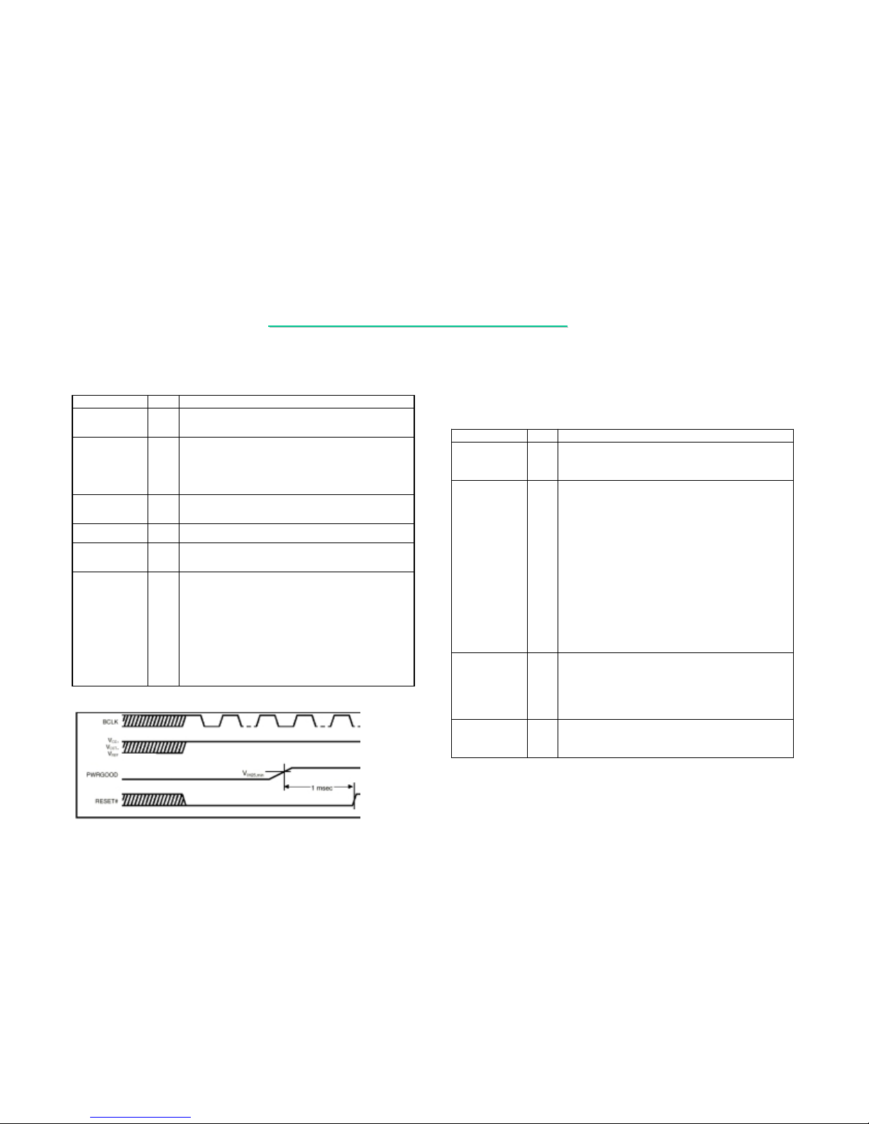
PWRGOOD (Power Good) is a 2.5-V tolerant input. The processor
requires this signal to be a clean indication that clocks and the power
supplies (Vcc, V ccT, etc.) are stable and with in their specific ations.
Clean implies that the signal will remain low, (capable of s inking
leakage current) and wi thout glitches, from the time that the power
supplies are turn ed on, until they come within specification. The
signal will then transition monotonically to a high (2.5V) state. Figure
26 illustrates the relationship of PWRGOOD to other system signa ls.
PWRGOOD can be driven inactive at any time, but clocks and power
must again be stable before the rising edge of PWRGOOD. It m ust
also meet the minimum pulse width specified in Table 17 (Section
3.7) and be followed by a 1 ms RESET# pulse.
PWRGOOD Relationship at Power On
Signal Name I/O Signal Description
REQ[4:0]# I/O
GTL+
The REQ[4:0]# (Request Command) signals must be conn ected to the
appropriate pins/balls on both agents on the system bus. They are
asserted by the current bus owner when it drives A[35:3]# to define
the currently active transaction type.
RESET# I
GTL+
Asserting the RESET# signal resets the processor to a known state
and invalidates th e L1 and L2 caches without writing back Modified
(M state) lines. For a power-on type reset, RESET# must stay active
for at least 1 msec after Vcc and BCLK have reached their proper DC
and AC specifications and after PWRGOOD has been asserted. When
observing active RESET# , all bus agents will deassert their outputs
within two clocks. R ESET# is the only GTL+ signal that does
not have on-die GTL+ termination. A 56.2
&1% terminating re sis to r
connected to Vc cT is required.
A number of bus signals are sampled at the active-to-inactive
transition of RESET# for the power-on configuration. The
configuration options are described in Section 4 and in the
Pentium II
Processor Developer’s Manual
.
Unless its outputs are tri-stated during power-on configuration, after
an active-to-inactive transition of RESET#, the processor optionally
executes its bui lt-in self-test (BIST) and begins program execution at
reset-vector 000FFFF0H or FFFFFFF0H. RESET# must be connected
to the appropriate pins/balls on both agents on the system bus.
RP# I/O
GTL+
The RP# (Request Parity) signal is driven by the request initiator and
provides parity protection on ADS# and REQ[4:0]#. RP# sh ould be
connected to the appropriate pins/balls on both agents on the system
bus.
A correct parity signal is high if an even number of covered signals
are low and low if an odd number of covered signals are low. This
definition allows parity to be high when all covered signals are high.
RS[2:0]# I
GTL+
The RS[2:0]# (Response Status) signals are driven by the response
agent (the agent responsible for completion of the curren t transaction)
and must be connected to the appropriate pins/balls on both agents on
the system bus.
4. PIN DESCRIPTIONS OF MAJOR COMPONENTS
4.1 Pentium III/Celeron FC-PGA2 CPU
Page 52
51
7521
7521
N/B MAINTENANCE
N/B MAINTENANCE
PWRGOOD Relationship at Power On
Signal Name I/O Signal Description
RSP# I
GTL+
The RSP# (Response Parity) signal is driven by the response agent
(the agent responsible for completion of the current transaction)
during assertion of RS[2 :0]#. RSP# provides parity pr otection for
RS[2:0]#. RSP# should be connected to th e appropriate pins/balls on
both agents on the system bus.
A correct parity signal is high if an even number of covered signals
are low, and it is low if an odd number of covered signals are low.
During Idle state of RS[2:0]# (RS[2:0]#=000), RSP# is also high
since it is not driven by any agent gu aranteeing correct parity.
RSVD TBD The RSVD (Reserved) signal is currently unimplemented but is
reserved for future use. Leave this signal unconnected. Intel
recommends that a routing channel for this signal be allocated.
RTTIMPEDP Analog The RTTIMPEDP (RTT Impedance/PMOS) signal is used to
configure the on-die GTL+ termination. Connect the RTTIMPEDP
signal to VSS with a 56.2-
&, 1% resistor.
SLP# I
1.5V
Tol era nt
The SLP# (Sleep) signal, when a sserted in the Stop Grant state,
causes the proces sor to enter the Sleep state. During the Sleep state,
the processor stops providing internal clock signals to all units,
leaving only the Pha se-Locked Loop (PLL) still running. The
processor will not recognize snoop and interrupts in the Sleep state.
The processor will only recognize changes in the SLP#, S TP CLK#
and RESET# signals while in the Sl eep state. If SLP# is deasserted,
the processor exits Sleep state and returns to the Stop Grant state in
which it restarts its internal clock to the bus and
APIC processor units.
SMI# I
1.5V
Tol era nt
The SMI# (System Management Interrupt) is asserted asynchronously
by system logic. On accepting a System Management Interrupt, the
processor saves t he current stat e and enters System Ma nagement
Mode (SMM). An SMI Acknowledge transaction is issued, and the
processor begins program execution from the SMM handler.
STPCLK# I
1.5V
Tol era nt
The STPCLK# (Stop Clock) signal, when asserted, causes the
processor to enter a low-power Stop Grant state. The processor issues
a Stop Grant Acknowledge special transaction and stops providing
internal clock signals to all units except the bus and APIC units. The
processor continues to snoop bus transactions and service interrupts
while in the Stop Gra nt state. When STPCLK# is deass erted, the
processor restarts its internal clock to all units and resumes execution.
The assertion of STPCLK# has no affect on the bus clock.
TCK I
1.5V
Tol era nt
The TCK (Test Clock) signal provides the clock input for the test bus
(also known as the test access port).
Signal Name I/O Signal Description
TDI I
1.5V
Tol era nt
The TDI (Test Data In) signal transfers serial test data to the
processor. TDI provides the serial input needed for JTAG support.
TDO O
1.5V
Tol era nt
Open-
drain
The TDO (Test Data Out) signal transfers serial test data from the
processor. TDO provides the serial output needed for JTAG support.
TESTHI I
1.5V
Tol era nt
The TESTHI (Test input High) is used during processor test and
needs to be pulled high during normal operation.
TESTLO[2:1] I
1.5V
Tol era nt
The TESTLO[2:1] (Test input Low) signals are used during proc essor
test and needs to be pulled to ground during normal operation.
TESTP An alog The TESTP (Test Point) signals are connected to Vcc and Vss at
opposite ends of the die. These signals can be used to monitor the Vcc
level on the die. Route the TESTP signals to test points or leave them
unconnected. Do not sh ort the TESTP signals together.
THERMDA,
THERMDC
Analog The THERMDA (Thermal Diode Anode) and THERMDC (Thermal
Diode Cathode) signals connect to the an ode and cathode of the ondie thermal diode.
TMS I
1.5V
Tol era nt
The TMS (Test Mode Select) signal is a JTAG support signal used by
debug tools.
TRDY# I
GTL+
The TRDY# (Target Ready) signal is asserted by the target to indicate
that the target is ready to receive write or implicit write-back data
transfer. TRDY# must be c onnected to the appropriate pins/ba lls on
both agents on the system bus.
TRST# I
1.5V
Tol era nt
The TRST# (Test Reset) signal resets the Test Access Port (TAP)
logic. The mobile Pentium III processors do not self-reset during
power on; therefore, it is necessary to drive this signal low during
power-on reset.
4. PIN DESCRIPTIONS OF MAJOR COMPONENTS
4.1 Pentium III/Celeron FC-PGA2 CPU
Page 53

52
7521
7521
N/B MAINTENANCE
N/B MAINTENANCE
PWRGOOD Relationship at Power On
Signal Name I/O Signal Description
VID[4:0] O -
Open-
drain
The VID[4:0] (Voltage ID) pins/balls can be used to support
automatic selection of power supply voltages. These pins/balls are not
signals, they are eit her an open circuit or a short to VSS on the
processor substrate. The combination of opens and shorts encodes the
voltage required by the processor. External to pull-ups are required to
sense the encoded VID. For processors that have Intel Sp eedStep
technology enabled, VID[4:0] encode the voltage required in the
battery-optimized mode. VID[4:0] are needed to cleanly support
voltage specification changes on mobile Pentium III processors. The
voltage encoded by VID[4:0] is defined in Table 39. A "1" in this
table refers to an open pin/ball and a "0" refers to a short to VSS. The
power supply must provide the requested voltage or disable itself.
Please note that in order to implement VID on the BGA2 package,
some VID[4:0] balls may be depopulated. For the BGA2 package, a
"1" in Table 39 implies that the corresponding VID ball is
depopulated, while a "0" implies that the corresponding VID ball is
not depopulated.
But on the Micro-PGA2 package, VID[4:0] pins are not depopulated.
4. PIN DESCRIPTIONS OF MAJOR COMPONENTS
4.1 Pentium III/Celeron FC-PGA2 CPU
Page 54
53
7521
7521
N/B MAINTENANCE
N/B MAINTENANCE
4. Pin Descriptions Of Major Components
4.2 SiS630 Slot 1/Socket 370 2D/3D Ultra-AGP™ Single Chipset
Host Bus Interface
Name Tolerance Power
Plane
Type
Attr
Description
CPUCLK 3.3V/5V MAIN I Host Clock :
ADS# 1.5V MAIN I/O
GTL+
Address Strobe : Address Strobe is driven by CPU to
indicate the start of a CPU bus cycle.
HREQ[4:0]# 1.5V MAIN I/O
GTL+
Request Command: HREQ[4:0]# are used to define
each transaction type during the clock when ADS# is
asserted and the c lock after ADS# is ass erted.
BREQ0# 1.5V MAIN O
GTL+
Symmetric Agent Bus Request: BREQ0# is driven
by the symmetric agent to request for the bus.
BNR# 1.5V MAIN I/O
GTL+
Block Next Request: This signal can be driven
asserted by any bus agent to block further requests
being pipelined.
HLOCK# 1.5V MAIN I
GTL+
Host Lock : CPU asserts HLOCK# to indicate the
current bus cycle is locked.
HIT# 1.5V MAIN I/O
GTL+
Keeping a Non-Modified Cache Line:
HITM# 1.5V MAIN I/O
GTL+
Hits a Modified Cache Line: Hit Modifie d in di ca tes
the snoop cycle hits a modified line in the L1 cache of
CPU.
DEFER# 1.5V MAIN O
GTL+
Defer Tran sa ct i on Completion: SiS630 will use this
signal to indicate a retry response to host bus.
RS[2:0]# 1.5V MAIN O
GTL+
Response Status: RS[2:0]# are driven by the response
agent to indicate the transaction response type. The
following shows the response type.
RS[2:0] Response
000 Idle State
100 Reserved
001 Retry
101 No data
010 Reserved
110 Implicit Write-back
011 Reserved
111 Normal Data
HTRDY# 1.5V MAIN I/O
GTL+
Target Ready: During write cycles, response agent
will drive TRDY# to indicate the agent is ready to
accept data.
DRDY# 1.5V MAIN I/O
GTL+
Data Ready: DRDY# is driven by the bus owner
whenever the data is valid on the bus.
DBSY# 1.5V MAIN I/O
GTL+
Data Bus Busy: Whenever the data is not valid on the
bus with DRDY# is deserted, DBSY# is asserted to
hold the bus.
Name Tolerance Power
Plane
Type
Attr
Description
BPRI#
1.5V MAIN O
GTL+
Priority Agent Bus Request:
BPRI# is driven by th e
priority agent that wa nts to re qu es t the bus.
BPRI# has higher prior i ty tha n BREQ 0 # to access a bus.
CPURST#
1.5V MAIN O
GTL+
Host Bus Reset:
CPURST# is used to keep all the bus
agents in the same init ial state before valid cyc les issued.
HA[31:3]#
1.5V MAIN I/O
GTL+
Host Address Bus :
HD[63:0]#
1.5V MAIN I/O
GTL+
Host Data Bus :
FERR#
1.5V~5V MAIN I
Floating Point Error :
CPU will assert this signal upon a
floating point error occurring.
IGNE#
1.5V~5V MAIN OD
Ignore Numeric Error :
IGNE# is asserted to inform CPU
to ignore a numeric error.
Speed Trap for PII :
This pin will be forced to voltage
level according to the input value of MD41 or APC0h.4
during system reset period.
NMI
1.5V~5V MAIN OD
Non-Maskable Interrupt :
A rising edge on NMI will
trigger a non-maskable interrupt to CPU. Speed Trap for
PII : This pin will be forced to voltage level according to
the input value of MD44 or APC0h.7 during system reset
period.
INTR
1.5V~5V MAIN OD
Interrupt Request :
High-level voltage of this signal
indicates the CPU that there is outstandin g in ter rupt(s)
needed to be serviced.
Speed Trap for PII :
This pin will be forced to voltage
level according to the input value of MD43 or APC0h.6
during system reset period.
CPUSLP#
1.5V~5V MAIN OD
CPU Sleep :
SiS630 can optiona ll y as sert CPUSLP# to
force the CPU into deep sleep mode when going to S2 state.
STPCLK#
1.5V~5V MAIN OD
Stop Clock :
STPCLK# will be asserted to inhibit or
throttle CPU activities upon a pre-defined power
management event occu rs.
SMI#
1.5V~5V MAIN OD
System Management Interrupt :
SMI# will be asserted
when a pre-defined power management event occurs.
Page 55
54
7521
7521
N/B MAINTENANCE
N/B MAINTENANCE
DRAM Controller
Name Tolerance Power
Plane
Type
Attr
Description
SDCLK 3.3V/5V MAIN I SDRAM Clock Input
MD[63:0] 3.3V MAIN I/O System Memory Data Bus
MA[14:0] 3.3V MAIN O System Memory Address Bus
CSA[5:0]# 3.3V MAIN O SDRAM Chip Select
CSB[5:0]# 3.3V MAIN O SDRAM Chip Select Signals
(Duplicated Copy)
DQM[7:0]# 3.3V MAIN O SDRAM Input/Output Data Mask
WE# 3.3V MAIN O SDRAM Write Enable
SRAS# 3.3V MAIN O SDRAM Row Address Strobe
SCAS# 3.3V MAIN O SDRAM Column Address Strobe
CKE 3.3V AUX O SDRAM Clock Enable
During Suspend-to-DRAM mode
(ACPI S2 or S3 state), SDRAM can
be put into self-refresh mode by
asserting CKE.
Host Bus Interface
Name Tolerance Power
Plane
Type
Attr
Description
INIT# 1.5V~5V MAIN OD Initialization : INIT is used to re-start the CPU
without flushing its internal caches and registers. In
Pentium II platform it is active high. This sign al
requires an external pull-up resistor tied to 3.3V.
A20M# 1.5V~5V MAIN OD Address 20 Mask : When A20M# is asserted, the
CPU A20 signal will be forced to "0".
Speed Trap for PII : This pin will be forced to
voltage level according to the input value of MD42 or
APC0h.5 during system reset period.
Name Tolerance Power
Plane
Type
Attr
Description
AD[31:0]
3.3V/5V MA IN I/O
PCI Address /Data Bus:
In address phase:
1.When the SiS Chip is a PCI bus m aster , AD [ 31:0]
are ou tput signal s.
2.When the SiS Chip is a PCI target, AD[31:0] are
input signals.
In data phase:
1.
When th e SiS Chip is a t ar g et o f a memory
read/write cycle, AD[31:0] are floating.
2.
When th e SiS Ch ip is a t ar g et o f a c o n figu ra tion o r
an I/O cycle, AD[31:0] are output signals in a
read cycle, and input signals in a write cycle.
PAR
3.3V/5V MA IN I/O
Parity :
SiS630 drives out Even Parity covering AD[31:0] and C/BE[3:0]#. It
does not check the input parity signal.
FRAME#
3.3V/5V MA IN I/O
Frame#:
FRAM E # is an output whe n the SiS C h ip is a PCI bus master. The SiS
Chip drives FRAME# to indicate the beginning and duration of an access.
When the SiS C hip is a PC I slave device, FRAME# is an input signal.
IRDY #
3.3V/5V MA IN I/O
Initia tor Read y :
IRDY# is an output when the SiS
Chip is a PCI bus m as ter . The assertion of IR D Y# indicates the current PCI bus
master's ability to
complete the current data phase of the transaction. For a read cycle, IRDY#
indicates that the PCI bus
master is prepared to accept the read data on the following rising edge of the
PCI clock. For a write
cycle, IRDY# indicates that the bus master has driven valid data on the PCI
bus. When the SiS Chi p is a
PCI slave, IRDY# is an inp ut pin.
TRDY#
3.3V/5V MA IN I/O
Tar get Re ady :
TRDY # is an output wh en the SiS
Chip is a PCI slave. The assertion of TRDY # in dicates the target agent's ability
to com p lete th e c ur re nt data phase of the tra nsa c tio n. F o r a read cycle, TRDY#
indicates that the target has driven valid data onto the PCI bus. For a write
cycle, TRDY# indicates that the target is prepared to accept data from the PCI
bus. When the SiS Chip is a PCI master, it is an i n p ut pin.
PCI Interface
Name Tolerance Power
Plane
Type
Attr
Description
PCICLK 3.3V/5V MAIN I PCI Clock : The PCICLK input provides the
fundamental timing and the in ternal operating
frequency for the SiS Chip. It runs at the same
frequency and skew of the PCI local bus.
C/BE[3:0]# 3.3V/5V MAIN I/O PCI Bus Command and Byte Enables: PCI Bu s
Command and Byte Enables define the PCI command
during the address phase of a PCI cycle, and the PCI
byte enables during the data phases. C/BE[3: 0] #
are outputs when th e SiS Chip is a PCI bus mas ter and
inputs when it is a PCI slave.
4. Pin Descriptions Of Major Components
4.2 SiS630 Slot 1/Socket 370 2D/3D Ultra-AGP™ Single Chipset
Page 56
55
7521
7521
N/B MAINTENANCE
N/B MAINTENANCE
PCI Interface
Name Tolerance Power
Plane
Type
Attr
Description
STOP# 3.3V/5V MAIN I/O Stop# : STOP# indicates that the bus master must start
terminating its current PCI bus cycle at the next
clock edge and release control of the PCI bus. STOP#
is used for disconnection, retry, and target-abortion
sequences on the PCI bus.
DEVSEL# 3.3V/5V MAIN I/O Device Select : As a PCI target, SiS Chip asserts
DEVSEL# by doing positive or subtractive decoding.
SiS Chip positively asserts DEVSEL# when the
DRAM address is being accessed by a PCI master, PCI
configuration registers or embedded controllers’
registers are being addressed, or the BIOS memory
space is being acc essed. The low 16 K I/O space and
low 16M memory space are responded subtractively.
The DEVESEL# is an input pin when SiS Chip is
acting as a PCI master. It is asserted by the addressed
agent to claim the current transaction.
PLOCK# 3.3V/5V MAIN I/O PCI Lock : When PLOCK# is sampled asserted at the
beginning of a PCI cycle, Si S630 considers itself being
locked and remains in the locked state until PLOCK#
is sampled and negated at the following PCI cycle.
PREQ[2:0]# 3.3V/5V MAIN I PCI Bus Request : PCI Bus Master Request Signals
PGNT[2:0]# 3.3V MAIN O PCI Bus Grant : PCI Bus Master Grant Signals
INT[A:D]# 3.3V/5V MAIN I PCI interrupt A,B,C,D : The PCI interrupts will be
connected to the inputs of the internal Interrupt
controller through the rerouting logic associated with
each PCI interrupt.
PCIRST# 3.3V AUX O PCI Bus Reset : PCIRST# will be asserted during
the period when PWROK is low, and will be kept on
asserting until about 2 4ms after PWROK goes high.
SERR# 3.3V/5V MAIN I System Error : When sampled active low, a non-
maskable interrupt (NMI) can be generated to CPU if
enabled.
Name Tolerance Power
Plane
Type
Attr
Description
IIOW[A:B]# 3.3V MAIN O Primary/Secondary Channel IOW# Signals
ICHRDY[A:B] 3.3V/5V MAIN I Primary/Secondary Channel ICHRDY# Signals
IDREQ[A:B] 3.3V/5V MAIN I Primary/Secondary Channel DMA Request Signals
IDACK[A:B]# 3.3V MAIN O Primary/Secondary Channel DMACK# Signals
IIRQ[A:B] 3.3V/5V MAIN I Primary/Secondary Channel Interrupt Signals
IDSAA[2:0] 3.3V MAIN O Primary Channel Address [2:0]
IDSAB[2:0] 3.3V MAIN O Secondary Channel Address [2:0]
CBLID[A:B] 3.3V/5V MAIN I Primary/Secondary Ultra-66 Cable ID
VGA Interface
Name Tolerance Power
Plane
Type
Attr
Description
HSYNC 3.3V MAIN O Horizontal Sync
VSYNC 3.3V MAIN O Vertical Sync
SSYNC 3.3V MAIN O Stereo Sync
DDCCLK 3.3V/5V MAIN I/O Display Data Channel Clock Line
DDCDATA 3.3V/5V MAIN I/O Display Data Channel Data Line
COMP MAIN AI Compensation Pin: Connect this pin to AVDD via a
0.1uF capacitor
RSET MAIN AI Reference Resistor: An external resistor is
connected bet ween the RSET pin and AGND to
control the
magnitude of the fu ll-scale current.
VREF MAIN AI Voltage Reference: Co n ne c t 0. 1 uF Capacitor to
Ground.
VCS# 3.3V MAIN I/O VGA Frame Buffer Cache Chip Select
ROUT MAIN AO Red Signal Output
GOUT MAIN AO Green Signal Output
BOUT MAIN AO Blue Signal Output
VBA1
VBCLK
PLPWDN#
3.3V MAIN O
I/O
O
Display Memory Bank Select: When 128bits
DRAM interface enable, it represents the Memory
Bank Select
Digital Video Clock Input: When Video Bridge
connected, it r epresents the Digital Video Clock
Input
Panel Power Down When external LCD transmitter
connected, it represents power down.
PCI IDE Interface
Name Tolerance Power
Plane
Type
Attr
Description
IDA[15:0] 3.3V/5V MAIN I/O Primary Channel Data Bus
IDB[15:0] 3.3V/5V MAIN I/O Secondary Channel Data Bus
IDECSA[1:0]# 3 .3V MAIN O Primary Channel CS[1:0]
IDECSB[1:0]# 3.3V MAIN O Secondary Channel CS[1:0]
IIOR[A:B]# 3.3V MAIN O Primary/Secondary Channel IOR# Signals
4. Pin Descriptions Of Major Components
4.2 SiS630 Slot 1/Socket 370 2D/3D Ultra-AGP™ Single Chipset
Page 57
56
7521
7521
N/B MAINTENANCE
N/B MAINTENANCE
VGA Interface
Name Tolerance Power
Plane
Type
Attr
Description
VMA11
VGCLK
3.3V MAIN OODisplay Memory Address bit 11 : When 128bits
DRAM interface enable, it represents the Memory
Address bit 11
Digital Video Clock Output: When Video Bridge
connected, it r epresents the Digital Video Clock
Output
VMA10
VBHCLK
3.3V MAIN OODisplay Memory Address bit 10: When 128bits
DRAM interface enable, it represents the Memory
Address bit 10
Control Clock Output: When Video Bridge
connected, it r epresents the Contro l Clock Output
VMD[63:60] 3.3V MAIN I/O Display Memory Data Bus bits [63:60]
VMD[59:52]
VBRGB[7:0]
3.3V MAIN I/OODisplay Memory Data Bus bits [59:52]
Digital Video Data bits [7:0]
VMD[51:49]
VBRGB[18:16]
3.3V MAIN I/OODisplay Memory Data Bus bits [51:49]
Digital Video Data bits [18:16]
VMD[48:44]
VBRGB[19:23]
3.3V MAIN I/OODisplay Memory Data Bus bits [48:44]
Digital Video Data bits [19:23]
VMD[43:42]
VBRGB[10:11]
3.3V MAIN I/OODisplay Memory Data Bus bits [43:42]
Digital Video Data bits [10:11]
VMD[41:40]
VBRGB[9:8]]
3.3V MAIN I/OODisplay Memory Data Bus bits [41:40]
Digital Video Data bits [9:8]
VMD[39:38]
VBRGB[13:12]
3.3V MAIN I/OODisplay Memory Data Bus bits [39:38]
Digital Video Data bits [13:12]
VMD[37:36]
VBRGB[14:15]
3.3V MAIN I/OODisplay Memory Data Bus bits [37:36]
Digital Video Data bits [14:15]
VMD35
VBBLANKN
3.3V MAIN I/OODisplay Memory Data Bus bit 35
Digital Video Display Enable
VMD[34:33]
TVCTL[0:1]
3.3V MAIN I/OODisplay Memory Data Bus bits [34:33]
Video Bridge Data Control bits [0:1]
VMD32
VBCAD
3.3V MAIN I/O
I/O
Display Memory Data Bus bit 32
Video Bridge Programming Control
VMD31
VBHSYNC
3.3V MAIN I/O
I/O
Display Memory Data Bus bit 31
Digital Video Horizontal Sync
VMD30
VBVSYNC
3.3V MAIN I/O
I/O
Display Memory Data Bus bit 30
Digital Video Vertical Sync
VMD29
DDC2CLK
3.3V MAIN I/O
I/O
Display Memory Data Bus bit 29
Second Display data channel clock line
VMD28
DDC2DATA
3.3V MAIN I/O
I/O
Display Memory Data Bus bit 28
Second Display data channel data line
VMD[27:0] 3.3V MAIN I/O Display Memory Data Bus bits [27:0]
Name Tolerance Power
Plane
Type
Attr
Description
VDQ M[7:0]
3.3V MAIN O Display M emory SDRA M Input /Output Mask
OSCI
3.3V/5V MAIN I External 14.318MHz Clock Input
ENTEST
3.3V/5V MAIN I Test Mode Enable
Power man agement Interface
Name Tolerance Power
Plane
Type
Attr
Description
ACPILED
<=5V AUX OD
ACPILED :
ACPIL E D ca n be us ed to c o ntrol the
blinking of an LED at the frequency of 1 Hz to indicate the system is at power
saving mode.
EXTSMI#
3.3V/5V MAIN I
External SMI#:
EXTSMI# can be used to generate
wakeup event, sleep event, or SCI/SMI#/GPEIRQ event to the ACPIcompatible power ma nagem e nt
unit.
PME#
3.3V/5V AUX I/O
PME# :
When the system is in pow er-dow n m od e, an active low event on
PME# will cause the PSON# to go low and hence turn on the power supply.
When
the system is in suspend mode, an active PME# event will cause the system
wakeup and generate an
SCI/SMI#/GPEIRQ.
PSON#
<=5V AUX OD
A T X Power O N/OFF cont rol:
PSO N# is used to control the on/off s tate o f
the ATX pow er supply. W hen the ATX power supply is in the OFF state, an
activated pow er - o n e vent will force the p o wer supply to ON state.
PWRBTN#
3.3V/5V AUX I
Power B u tton :
This s i gnal is from the power button
switch and will be m o nitored b y the A CPI- mpatible power manag ement unit
to switch the system betwee n w orkin g an d sleepin g states.
RING
3.3V/5V AUX I
Ring Ind icatio n :
An active R IN G pulse and lasting for more than 4ms will
cause a wakeup ev en t for system to w a ke from S1~S5.
4. Pin Descriptions Of Major Components
4.2 SiS630 Slot 1/Socket 370 2D/3D Ultra-AGP™ Single Chipset
Page 58
57
7521
7521
N/B MAINTENANCE
N/B MAINTENANCE
Power management Interface
Name Tolerance Power
Plane
Type
Attr
Description
THERM# 3.3V/5V MAIN I Thermal Detect : THERM# is connected to the
internal ACPI-compatible power management
unit as an indication of outstanding thermal event.
An active THERM# event can be used to generate
SCI/SMI#/GPEIRQ. If THERM# is activated for
more than 2 second, a thermal override even t will
occur and the system will enter CPU th ermal
throttling mode aut omatically.
GPIO[6:4] 3.3V/5V AUX I/O/OD General Purpose Input/Output [6:4]: Refer to GPIO
description.
SMBus Interface
Name Tolerance Power
Plane
Type
Attr
Description
SMBDAT
I2CDAT
3.3V/5V MAIN I/OD
I/OD
SMBus Data : SMBus data input/output pin.
I2C Data : I2C data input/output pin.
SMCLK
I2CCLK
3.3V/5V MAIN I/OD
I/OD
SMBus Clock : SMBus clock input/output pin.
I2C Clock : I2C clock input/output pin.
SMBALT#
I2CALT#
GPIO15
3.3V/5V AUX I/OD
I/OD
I/O/OD
SMBus Alert : This pin is used for SMBus de v ice to
wake up the system from sleep state or to generate
SCI/SMI#/GPEIRQ.
I2C Alert : This pin is used for I2C device to wake
up the system from sleep state or to generate
SCI/SMI#/GPEIRQ.
General Purpose Input/Output 15 : Refer to GPIO
description.
Keyboard controller Interface
Name Tolerance Power
Plane
Type
Attr
Description
KBDAT
GPIO10
3.3V/5V AUX I/OD
I/O/OD
Keyboard Dada : When the internal keyboard
controller is enabled, th is pi n is us ed as the keyboard
data signal.
General Purpose Input/Output 10 : Refer to GPIO
description.
KBCLK
GPIO11
3.3V/5V AUX I/OD
I/O/OD
Keyboard Clock : When the internal keyboard
controller is enabled, th is pi n is us ed as the keyboard
clock signal. General Purpose Input/Output 11 :
Refer to GPIO description.
Name Tolerance Power
Plane
Type
Attr
Description
PMDA T
GPIO12
3.3V/5V AUX I/OD
I/O/O D
PS2 Mouse Data:
When the internal keyboard and PS2 mouse controllers are
enab le d, th is p in is
used as PS2 mouse data signal.
General Purpose Input/Output 12 :
Refer to GPIO descrip tion.
PMCLK
GPIO13
3.3V/5V AUX I/OD
I/O/O D
PS2 Mouse Clock:
When the internal keyboard and PS2 m ouse controllers are
enabled, this pin is used as the PS2 mouse clock signal.
General Purpose Input/Output 13 :
Refer to GPIO descrip tion.
KLOCK#
GPIO14
3.3V/5V AUX I
I/O/O D
Keyboard L ock :
When K LO CK # is tied low, the internal keyboard controller
will not respond to
any key-strikes.
General Purpose Input/Output 14 :
Refer to GPIO descrip tion.
LPC Interface
Name Tolerance Power
Plane
Type
Attr
Description
LAD [3:0]
3.3V/5V M AIN I/O
LPC Address/Data Bu s :
LPC controller drives these four pins to tr a n s mit LPC
command, a ddress,
and data to LPC device.
LDRQ#
3.3V/5V M AIN I
LPC DMA Request 0:
This pin is used by LPC device to request DMA cycle.
LFRAME#
3.3V MAIN O
LPC Frame :
This pin is used to notify LPC device
that a start or a abort LPC cycle will occur.
SIRQ
3.3V/5V M AIN I/OD
Serial IRQ :
This signal is used as the serial IRQ
line sig nal.
4. Pin Descriptions Of Major Components
4.2 SiS630 Slot 1/Socket 370 2D/3D Ultra-AGP™ Single Chipset
Page 59
58
7521
7521
N/B MAINTENANCE
N/B MAINTENANCE
RTC Interface
Name Tolerance Power
Plane
Type
Attr
Description
AUXOK 1.8V RTC I Auxiliary Power OK : This signal is supplied from
the power source of resume well. It is also used to
reset the logic in resume power well. If there is no
auxiliary power source on the system, this pin should
be tied together with PWROK.
BATOK 1.8V RTC I Battery Power OK: When the internal RTC is
enabled, this signal is use d to in dicate that the powe r
of RTC well is stable. It is also used to reset the logic
in RTC well . If the inter n al RTC is disabl ed, this pin
should be tied low.
OSC32KHI 1.8V RTC I RTC 32.768 KHz Input : When internal RTC is
enabled, this pin provide s the 32.768 KHz clock
signal from external crystal or oscillator.
OSC32KHO <1.8V RTC O RTC 32.768 KHz Output : When internal RTC is
enabled, this pin shoul d be connected with the othe r
end of the 32.768 KHz crystal or left unconnect ed if
an oscillator is used.
PWROK 1.8V RTC I Main Power OK : A high-level input to this signal
indicates the power being supplied to the system is in
stable operating state. Durin g t he period of PWROK
being low, CPURST and PCIRST# will all be
asserted until after PWROK goes high for 24 ms.
AC’97 interface
Name Tolerance Power
Plane
Type
Attr
Description
AC_BITCLK 3.3V/5V MAIN I AC’97Bit Clock : This signal is a 12.288MHz
serial data clock, which is generated by primary
Codec.
AC_RESET# 3.3V AUX O AC’97 Reset : Hardware reset signal for external
Codecs.
AC_SDIN[1:0] 3.3V/5V AUX I AC’97 Serial Data input : Serial data input from
primary Codec and secondary Codec.
AC_SDOUT 3.3V MAIN O AC’97 Serial Data output : Serial data output to
Codecs.
AC_SYNC 3.3V MAIN O AC’97 Syncronization : This is a 48KHz signal,
which is used to syncroniz e the Co decs.
SPDIF
GPIO7
3.3V/5V MAIN O
I/O/OD
S/PDIF Transmitter Output
General Purpose Input/Output 7 :
Refer to GPIO description.
Fast Ethern et and H omenetworking interface
Name Tolerance Power
Plane
Type
Attr
Description
EECS
3.3V AUX O
Serial EEP R O M Chip Select :
This enables the EEPROM during loading of
the Ethernet configuration data.
EEDI
3.3V AUX O
Serial EE P ROM Da ta Inp u t :
During serial EEPROM access cycle, the
SiS6 30 will use this p in to serially w r ite OP codes, addresses an d d a ta into the
serial EEP R OM.
EEDO
GPIO3
3.3V/5V AUX I
I/O/OD
Serial EE P ROM Da ta O u tput :
During serial EEPROM access cycle, the
SiS630 will read the contents of the EEPROM serially through this pin.
Requires external pull-up resistor.
Gener a l Purpose Inpu t/Output 3 :
Refer to G P IO des cription .
EESK
3.3V AUX O
Serial EEP R O M Clock :
This pin pro vide s the c lock for the ser ial EE P R O M.
OSC25M H I
3.3V AUX I
PHY 25MHz Clock Input :
This pin is supplied the 25MHz clock signal input
from the external crystal or an oscillator.
PLEDO#
OC3#
GPIO8
3.3V AUX OD
O
I/O/OD
Programmable LED Output :
(A)Select 10/100 M b ps L A N Mode: This pin is used as an LIN K /A C T IV IT Y
indication output.
(B)Select Home Networking M ode: This pin is also an LINK/AC T IVITY
indication output.
OC3# :
When this pin is configured as OC3#, it can
detects USB Port 3 over current condition.
Gener a l Purpose Inpu t/Output 8 :
Refer to G P IO des cription .
REXT
AUX I
Tr an smit Current S et :
An external resistor connected between this pin and
GN D will set the ou tp ut cu rre n t lev el f or the twisted pair out pu ts .
TPIP
AU X I Twisted Pa ir Receive Positive Input
TPIN
AU X I Twisted Pa ir Receive Negative Inpu t
TPOP
AU X O Twiste d P air Transmit P o sitiv e O u tp u t
TPON
AUX O Twisted Pair Transmit Negative Output
HRTXRXP
AU X I/O Twiste d P air Transmit / Receive Pos itiv e Data
HRTXRXN
AU X I/O Twiste d P air Transmit / Receive Negative Data
4. Pin Descriptions Of Major Components
4.2 SiS630 Slot 1/Socket 370 2D/3D Ultra-AGP™ Single Chipset
Page 60
59
7521
7521
N/B MAINTENANCE
N/B MAINTENANCE
USB interface
Name Tolerance Power
Plane
Type
Attr
Description
CLK48M 3.3V/5V MAIN I USB 48 MHz clock input : This signal provides
the fundamental clock for the USB Controller.
OC0#
PCIREQ3#
GPIO0
3.3V/5V MAIN I
I
I/O/OD
USB Port 0 Over C urrent Detection : OC0# is
used to detect the over current condition of USB
Port 0.
External PCI Master Request 3: PCIREQ3# is
used for PCI Device on PCI Slot 3 t o as s ert its
request to hold PCI Bus.
General Purpose Input/Output 0 : Refer to GPIO
description.
OC1#
PCIGNT3#
GPIO1
3.3V/5V MAIN I
O
I/O/OD
USB Port 1 Over C urrent Detection : OC1# is
used to detect the over current condition of USB
Port 1.
External PCI Master Grant 3 : PCIGNT3# is
used to indicate PCI Device on PCI Slot 3 the PCI
Bus has been granted .
General Purpose Input/Output 1 : Refer to GPIO
description.
OC3#
LDRQ1#
GPIO2
3.3V/5V MAIN I
I
I/O/OD
USB Port 3 Over C urrent Detection: OC3# is
used to detect the over current condition of USB
Port 3.
LPC DMA Request 1 : LDRQ1# is the second
LPC DMA request signal used by LPC Device to
request DMA cycles.
General Purpose Input/Output 2 : Refer to GPIO
description.
USBP[4:0]P 3.3V AUX I/O USB Port [4:0] Positive Input/Output
USBP[4:0]N 3.3V AUX I/O USB Port [4:0] Negative Input/Output
Legacy I/o and Miscellaneous Signals
Name Tolerance Power
Plane
Type
Attr
Description
SPK 3.3V MAIN O Speaker output : The SPK is connected to the
system speaker.
Power and Ground Signals
Nam e Tolerance Power
Plane
Type
Attr
Description
VSS
GROUND 0V
IVDD
MAIN 1. 8V
IVDD (AUX)
AUX 1.8V
OVDD
(AU X )
AUX 3.3V
USBVDD
AUX 3.3V
RTCVDD
RTC 1.8 V
DCLKA VDD
MAIN 3. 3V
ECLKA V DD
MAIN 3. 3V
TXA VD D
AUX 3.3V
RXA VDD
AUX 3.3V
DACA VDD
MAIN 3. 3V
IDE AVDD
MAIN 1. 8V
SDA VDD
MAIN 3. 3V
CPUAVDD
MAIN 3. 3V
VTTB
MAIN 1. 5V
VSSQ
GROUND 0V
VTTA
MAIN 1. 5V
VCC3
MAIN 3. 3V
4. Pin Descriptions Of Major Components
4.2 SiS630 Slot 1/Socket 370 2D/3D Ultra-AGP™ Single Chipset
Page 61
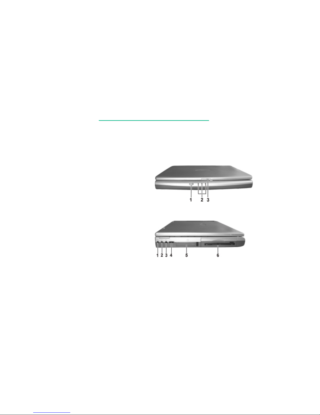
60
7521
7521
N/B MAINTENANCE
N/B MAINTENANCE
5 System View and Disassembly
5.1 System View
5.1.1 Front View
Mail-Received Button/Indicator
Power Indicators
Top Cover Latch
5.1.2 Left-Side View
Audio Input Connector
Microphone Connector
Audio Output Connector
Volume Control
PC Card Slots
Floppy Disk Drive
Page 62
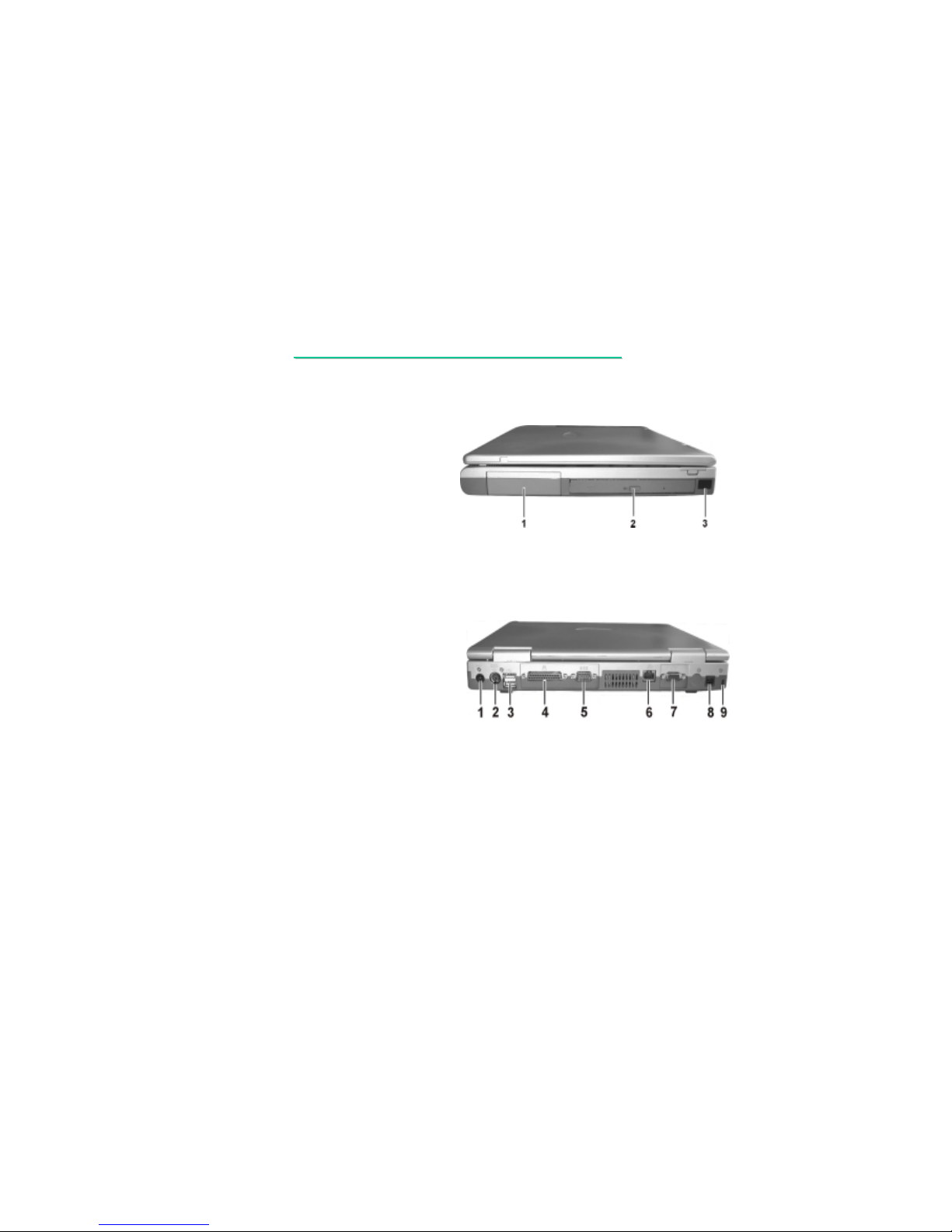
61
7521
7521
N/B MAINTENANCE
N/B MAINTENANCE
5.1.3 Right-Side View
Battery Pack
CD-ROM/DVD-ROM Drive
IR Port
5.1.4 Rear View
Power Connector
PS/2 Port
USB Ports
Parallel Port
Serial Port
RJ-45 Connector
VGA Port
RJ-11 Connector
Kensington Lock
Page 63
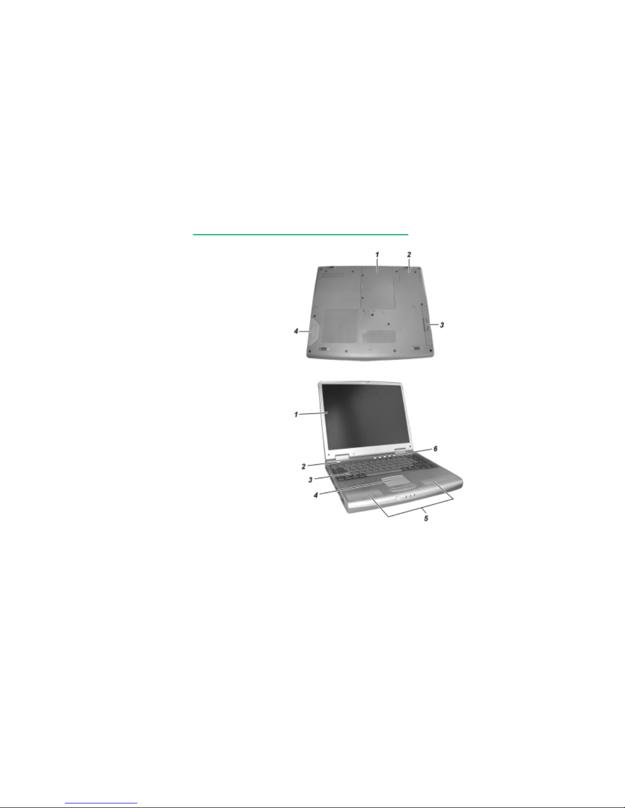
62
7521
7521
N/B MAINTENANCE
N/B MAINTENANCE
5.1.5 Bottom View
CPU Cover
Modem Card Cover
FDD/HDD Module
Battery Pack
5.1.6 Top-Open View
LCD Screen
Power Button
Keyboard
Touchpad
Stereo Speaker Set
Easy Start Buttons
Page 64

63
7521
7521
N/B MAINTENANCE
N/B MAINTENANCE
5.2 System Disassembly
The section discusses at length each major component for disassembly/reassembly and show corresponding
illustrations. Use the chart below to determine the disassembly sequence for removing components from the
notebook.
NOTE: Before you start to install/replace these modules, disconnect all peripheral devices and make sure the
notebook is not turned on or connected to AC power.
Modular Components
LCD Assembly Components
Base Unit Components
NOTEBOOK
5.2.1 Battery Pack
5.2.2 CPU
5.2.3 Modem Card
5.2.4 FDD/HDD Module
5.2.5 CD-ROM Drive
5.2.6 Keyboard
5.2.7 SO-DIMM
5.2.8 LCD Assembly
5.2.9 LCD Panel
5.2.10 Inverter Board
5.2.11 System Board
5.2.12 Touchpad
Page 65
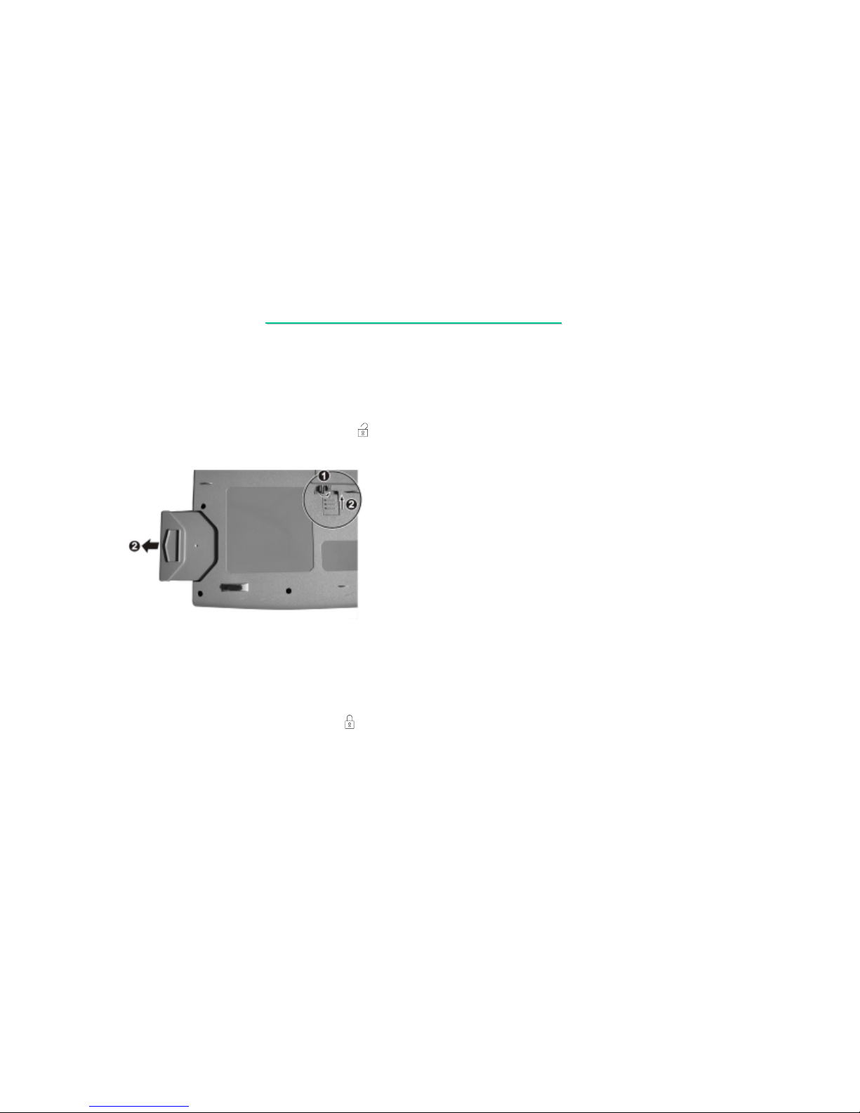
64
7521
7521
N/B MAINTENANCE
N/B MAINTENANCE
5.2.1 Battery Pack
Disassembly
1. Carefully put the notebook upside down.
2. Turn the locking button to the "unlock” ( ) position (), then slide and hold the latch in the
unlock position and pull the battery pack out of the compartment ().(figure 5-1)
Figure 5-1
Reassembly
1. Push the battery pack into the compartment. The battery pack should be correctly connected
when you hear a clicking sound.
2. Turn the locking button to the "lock” ( ) position.
Page 66
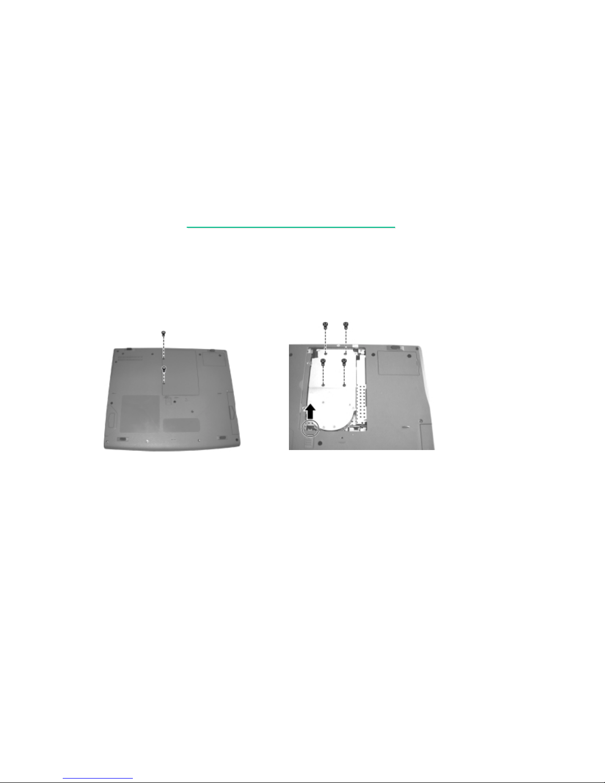
65
7521
7521
N/B MAINTENANCE
N/B MAINTENANCE
5.2.2 CPU
Disassembly
1. Carefully put the notebook upside down.
2. Remove two screws locking the CPU compartment cover, and then lift the cover up. (figure 5-2)
Figure 5-2 Figure 5-3
3. Remove four screws fastening the heatsink and disconnect the fan’s power cord to free the heatsink
from the CPU module. (figure 5-3)
Page 67
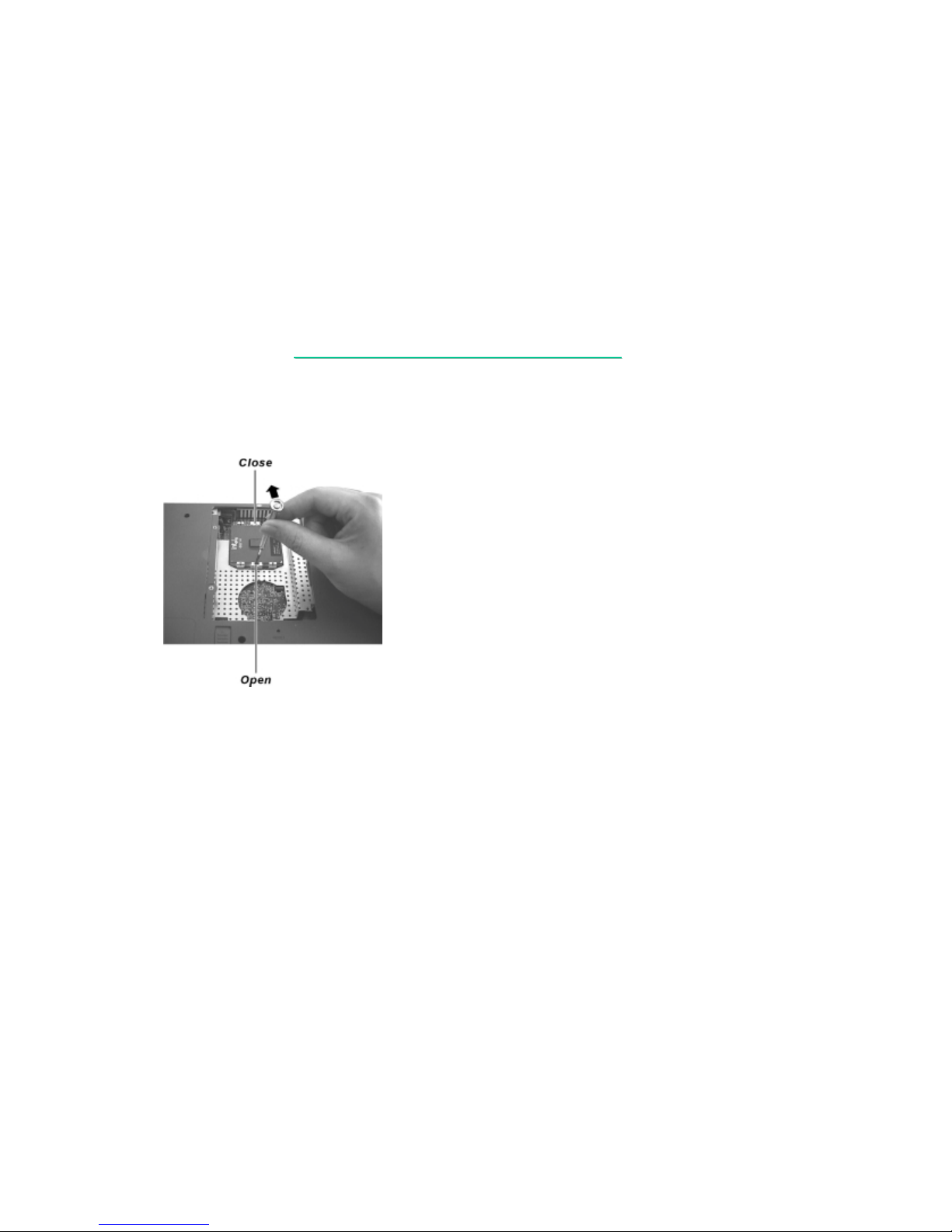
66
7521
7521
N/B MAINTENANCE
N/B MAINTENANCE
4. Insert a minus screwdriver 101 (JIS standard) into the “OPEN” hole of the socket,
and push the screwdriver toward the CPU to free the CPU. Now you can take out the CPU
from the socket. (figure 5-4)
Figure 5-4
Reassembly
1. Align the arrowhead corner of the CPU with the beveled corner of the socket, and insert the CPU pins
into the holes. Insert the flat screwdriver into the “CLOSE” hole of the socket, and push the screwdriver
toward the CPU to secure the CPU in place.
2. Connect the fan’s power cord to the system board, fit the heatsink onto the top of the CPU
and secure with four screws.
3. Replace the CPU compartment cover and secure with two screws.
Page 68
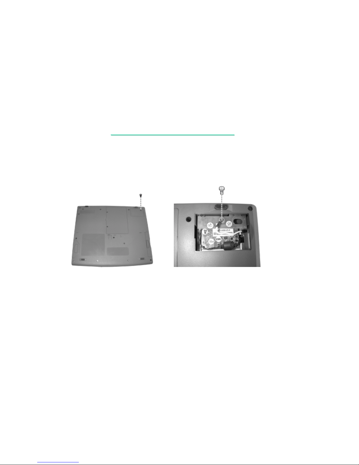
67
7521
7521
N/B MAINTENANCE
N/B MAINTENANCE
5.2.3 Modem Card
Disassembly
1. Carefully put the notebook upside down.
2. Remove one screw locking the modem card compartment cover, and then lift the cover up. (figure 5-5)
Figure 5-5 Figure 5-6
3. Remove one screw fastening the connector board and the grounding cable. (figure 5-6)
Page 69
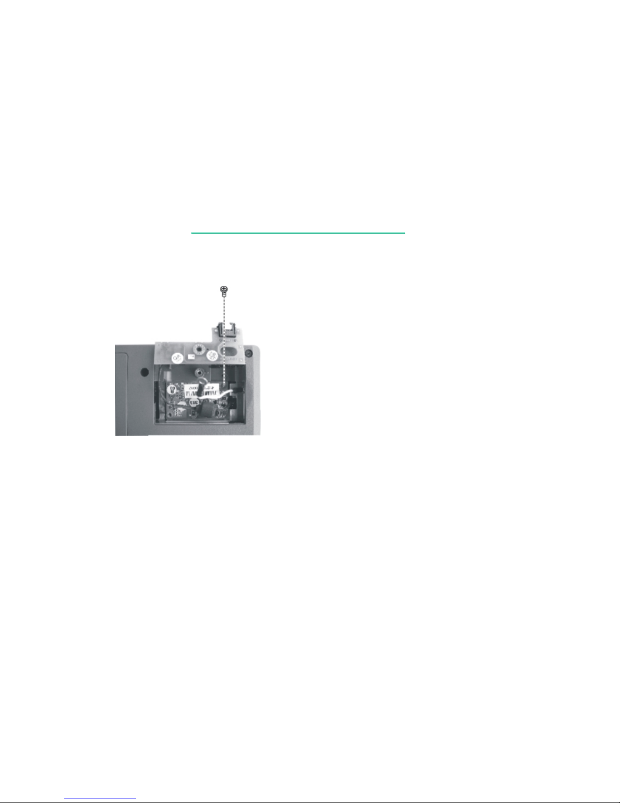
68
7521
7521
N/B MAINTENANCE
N/B MAINTENANCE
4. Slightly lift up the connector board, and then remove one screw fastening the modem card.
Now you can take out the modem card from the compartment. (figure 5-7)
Figure 5-7
Reassembly
1. Reconnect the modem card into the system board and secure with two screws.
2. Hold the connector board an angle so that the phone line connector is pointed towards the opening
on the notebook. Insert the connector into the opening and secure with a screw which fastening
both the connector board and the grounding cable.
3. Replace the compartment cover and secure with one screw.
Page 70
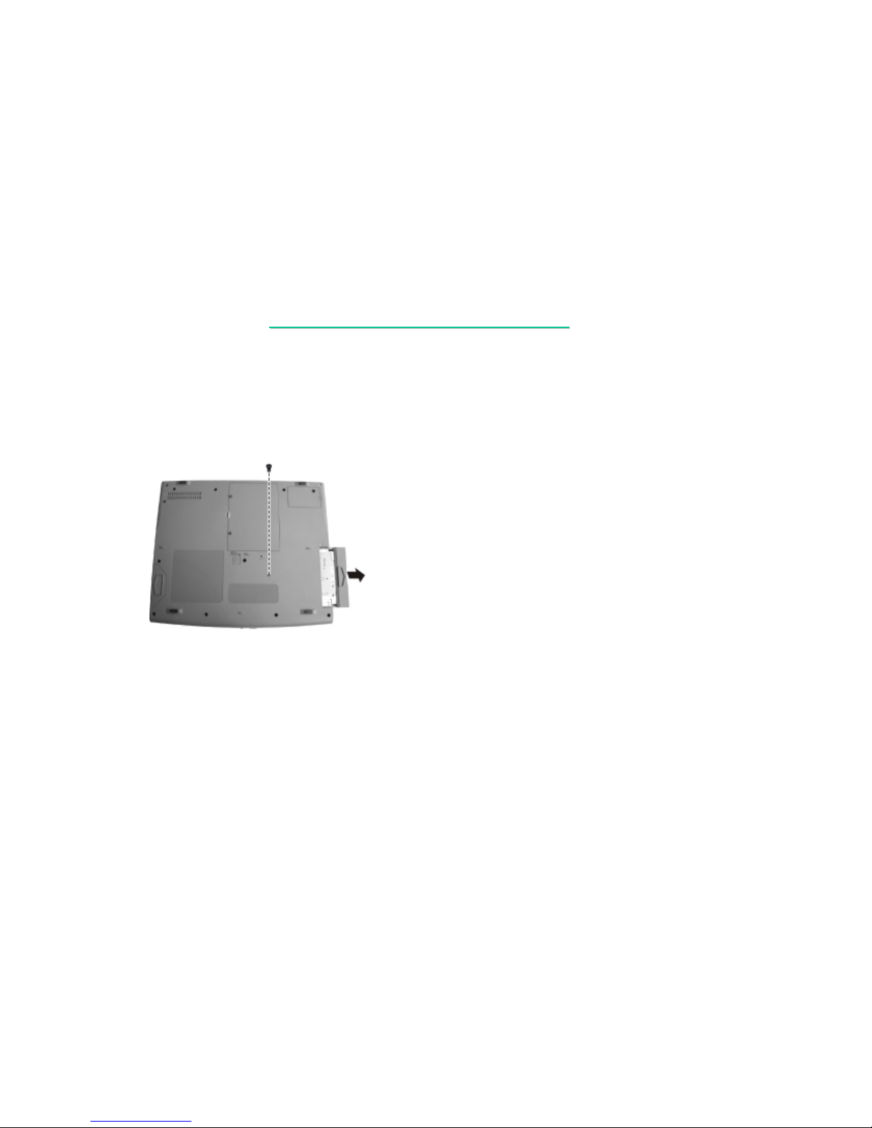
69
7521
7521
N/B MAINTENANCE
N/B MAINTENANCE
5.2.4 FDD/HDD Module
Disassembly
1. Carefully put the notebook upside down.
2. Remove one screw and slide the FDD/HDD module out of the compartment. (figure 5-8)
Figure 5-8
Page 71
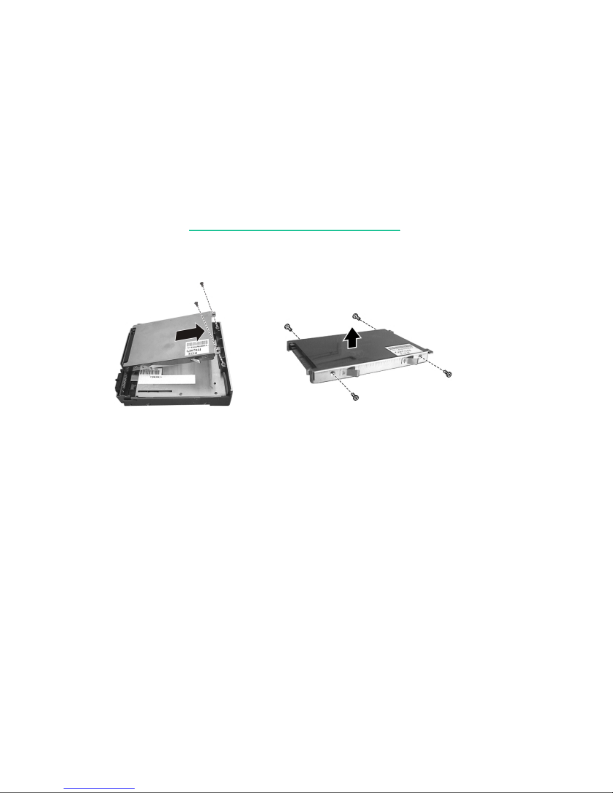
70
7521
7521
N/B MAINTENANCE
N/B MAINTENANCE
3. To take the hard disk drive apart, remove two screws of the hard disk. Then lift the hard disk up
and unplug the connector to remove it. (figure 5-9)
Figure 5-9 Figure 5-10
4. Remove four screws to separate the hard disk drive from the metal shield. (figure 5-10)
Reassembly
1. To install the hard disk drive, place it in the bracket and secure with four screws.
2. Connect the hard disk to the connector on the FDD/HDD module and secure with two screws.
3. Slide the FDD/HDD module into the compartment and secure with one screw.
Page 72
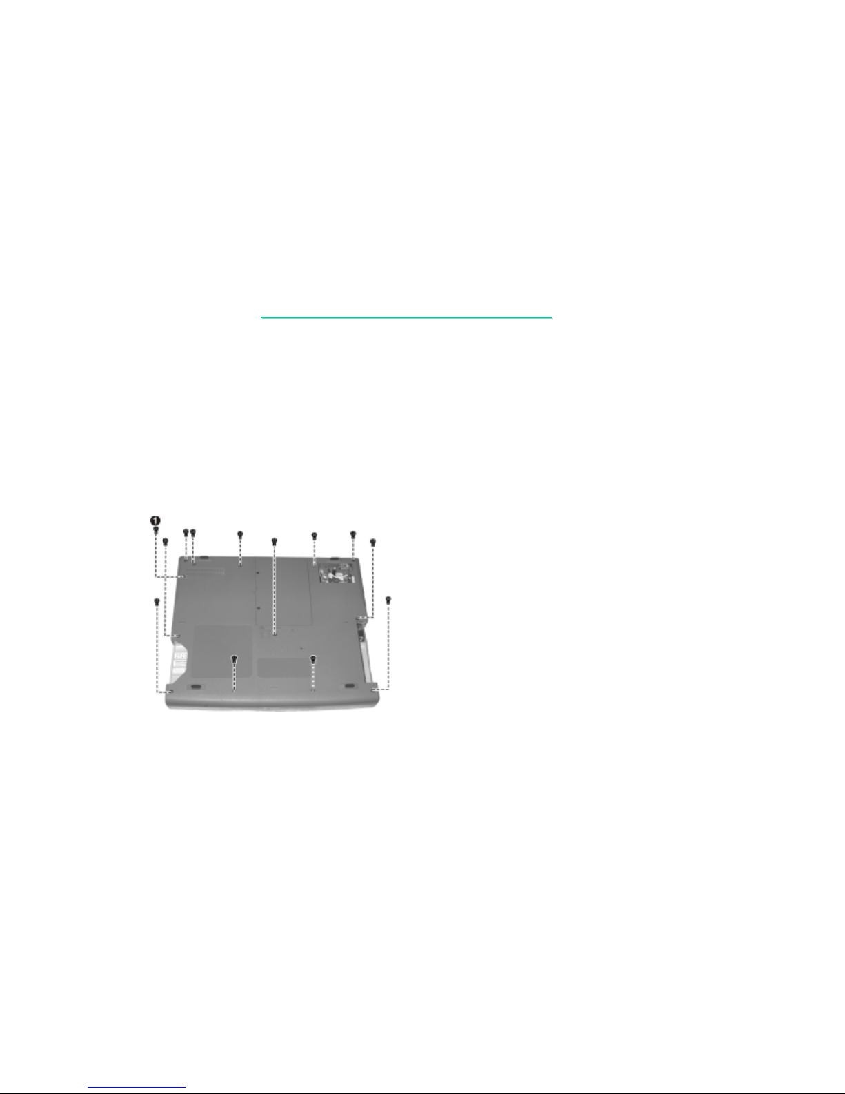
71
7521
7521
N/B MAINTENANCE
N/B MAINTENANCE
5.2.5 CD-ROM Drive
Disassembly
1. Carefully put the notebook upside down.
2. Remove the battery pack. (See section 5.2.1 Disassembly.)
3. Remove the modem card. (See section 5.2.3 Disassembly.)
4. Remove the FDD/HDD module. (See step 2 in section 5.2.4 Disassembly.)
5. Remove one screw locking the CD-ROM (), and then the other twelve screws
locking the base unit frame. (figure 5-11) Now you can lift the base unit frame up.
Figure 5-11
Page 73
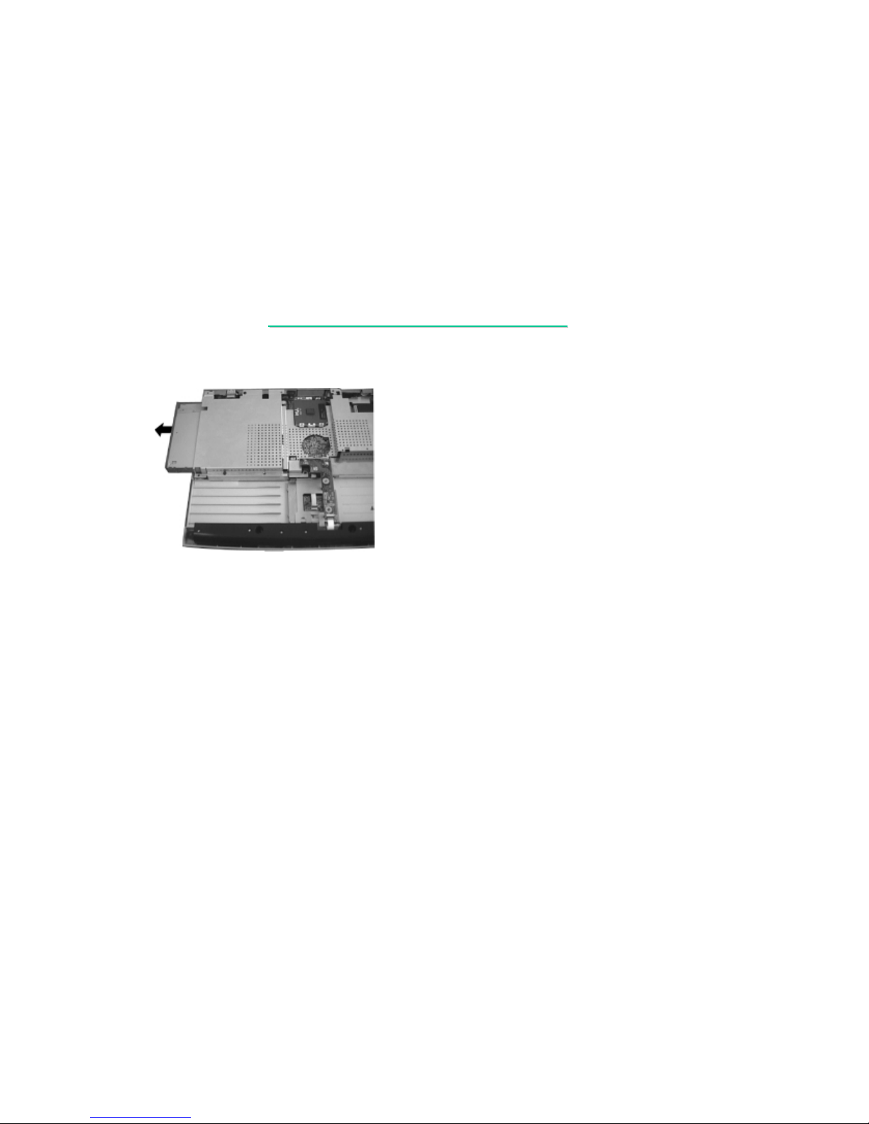
72
7521
7521
N/B MAINTENANCE
N/B MAINTENANCE
6. Hold the CD-ROM drive and slide it outward carefully. (figure 5-12).
Figure 5-12
Reassembly
1. Push the CD-ROM drive into the compartment.
2. Replace the base unit frame and secure with thirteen screws (includes one locking the CD-ROM drive).
3. Replace the FDD/HDD module. (See section 5.2.4 Reassembly.)
4. Replace the modem card. (See section 5.2.3 Reassembly.)
5. Replace the modem card. (See section 5.2.3 Reassembly.)
6. Replace the battery pack. (See section 5.2.1 Reassembly.)
Page 74
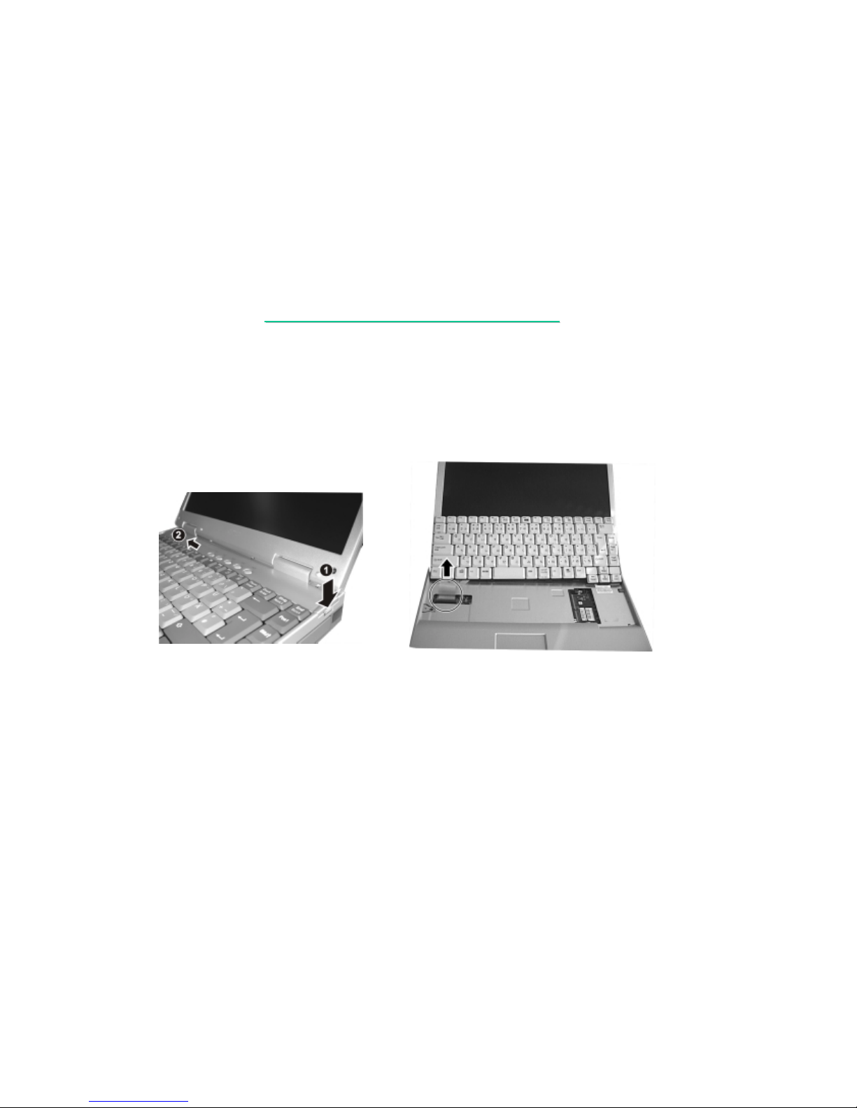
73
7521
7521
N/B MAINTENANCE
N/B MAINTENANCE
5.2.6 Keyboard
Disassembly
1. Open the top cover.
2. Press the locking latch downward to unlatch the Easy Start panel () , push it leftward and
lift it up from the left side (). (figure 5-13 )
Figure 5-13 Figure 5-14
3. Slightly lift up the keyboard and disconnect the cable from the system board to detach the keyboard.
Reassembly
1. Reconnect the keyboard cable and fit the keyboard back into place.
2. Replace the Easy Start panel.
Page 75
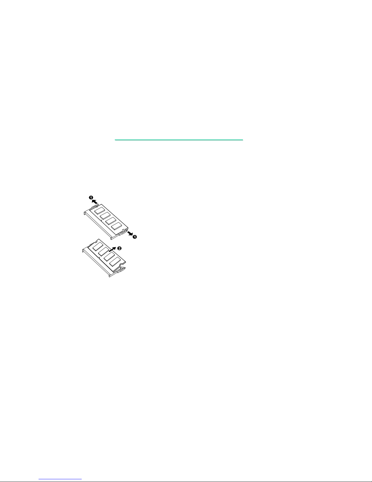
74
7521
7521
N/B MAINTENANCE
N/B MAINTENANCE
5.2.7 SO-DIMM
Disassembly
1. Remove the keyboard to access the SO-DIMM sockets. (See section 5.2.6 Disassembly.)
2. Pull the retaining clips outwards () and remove the SO-DIMM (). (figure 5-15)
Figure 5-15
Reassembly
1. To install the SO-DIMM, match the SO-DIMM's notched part with the socket's projected part
and firmly insert the SO-DIMM into the socket at 20-degree angle. Then push down until the
retaining clips lock the SO-DIMM into position.
2. Replace the keyboard and the Easy Start panel. (See section 5.2.6 Reassembly.)
Page 76
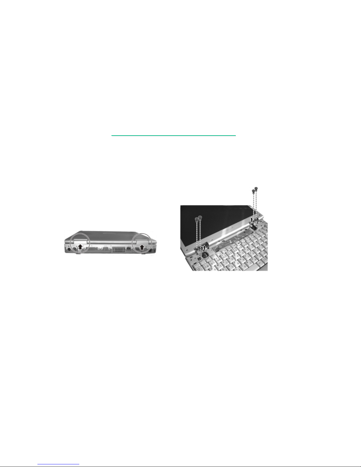
75
7521
7521
N/B MAINTENANCE
N/B MAINTENANCE
5.2.8 LCD Assembly
Disassembly
1. Open the top cover and remove the Easy Start panel. (See steps 1 to 2 in section 5.2.6 Disassembly.)
2. Remove the two hinge covers by inserting a flat screwdriver to the rear of the cover and pry the
cover out. (figure 5-16)
Figure 5-16 Figure 5-17
3. Open the top cover. Unplug the three cable connectors coming from the LCD assembly,
and remove four screws of the hinges. Now you can separate the LCD assembly from the
base unit. (figure 5-17)
Page 77

76
7521
7521
N/B MAINTENANCE
N/B MAINTENANCE
Reassembly
1. Attach the LCD assembly to the base unit and secure with four screws on the hinges.
2. Reconnect the LCD cable connectors to the system board.
3. Replace the two hinge covers.
4. Replace the Easy Start panel.
Page 78
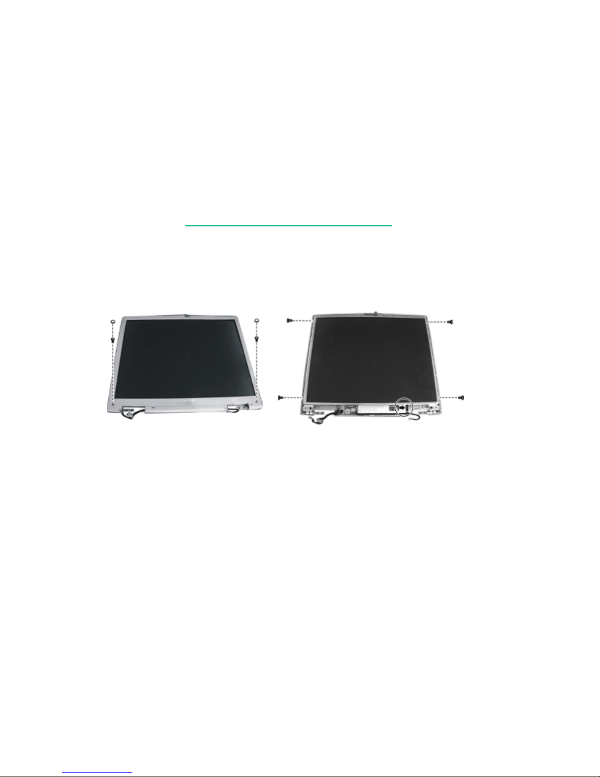
77
7521
7521
N/B MAINTENANCE
N/B MAINTENANCE
5.2.9 LCD Panel
Disassembly
1. Remove the LCD assembly. (See section 5.2.8 Disassembly.)
2. Remove the two rubber pads and two screws on the lower part of the panel. (figure 5-18)
Figure 5-18 Figure 5-19
3. Insert a flat screwdriver to the lower part of the frame and gently pry the frame out.
Repeat the process until the frame is completely separated from the housing.
4. Remove the four screws on the two sides of the LCD panel, and unplug the cable from
the inverter board. (figure 5-19)
Reassembly
1. Fit the LCD panel back into place and secure with four screws, and reconnect the cable to the inverter board.
2. Fit the LCD frame back into the housing and replace the two screws and two rubber pads.
3. Replace the LCD assembly. (See section 5.2.8 Reassembly.)
Page 79
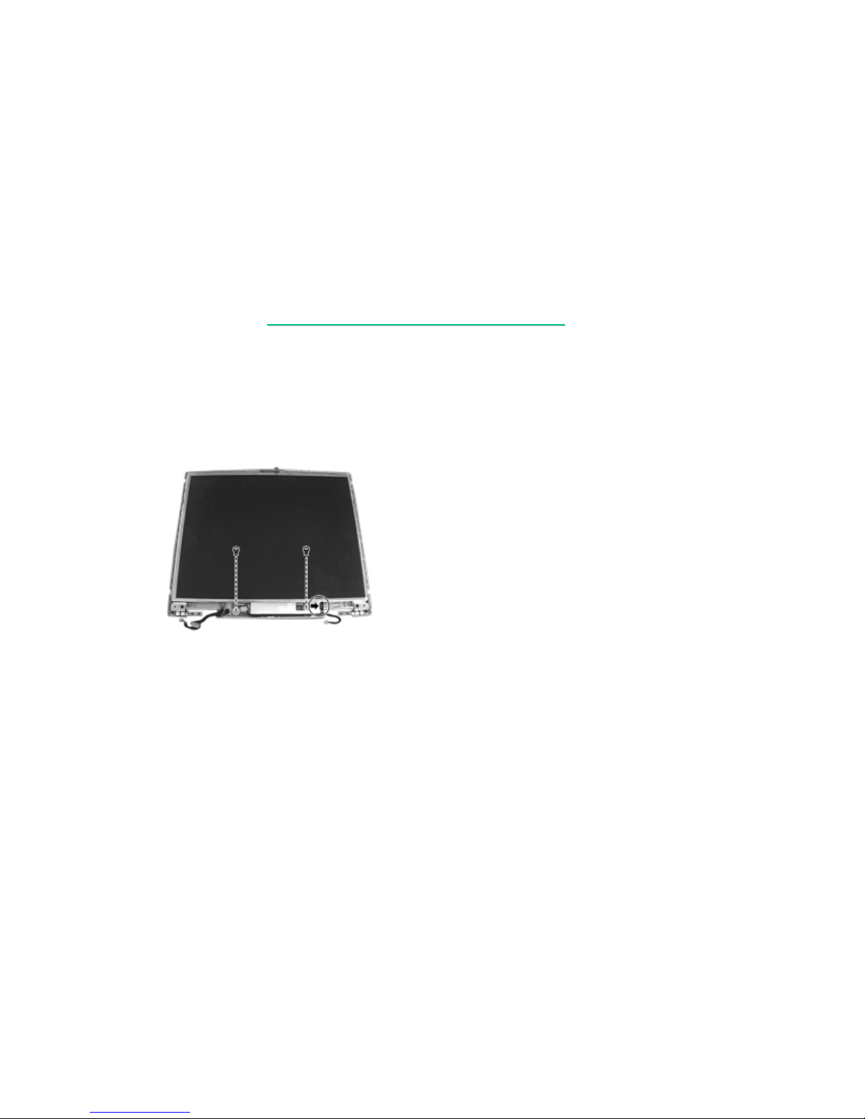
78
7521
7521
N/B MAINTENANCE
N/B MAINTENANCE
5.2.10 Inverter Board
Disassembly
1. Remove the LCD assembly and detach the LCD frame (see instructions in previous two sections).
2. To remove the inverter board at the bottom side of the LCD assembly, unplug the cable and
remove the two screws. (figure 5-20)
Figure 5-20
Reassembly
1. Fit the inverter board back into place and secure with two screws.
2. Reconnect the cables.
3. Replace the LCD frame. (See section 5.2.9 Reassembly.)
4. Replace the LCD assembly. (See section 5.2.8 Reassembly.)
Page 80
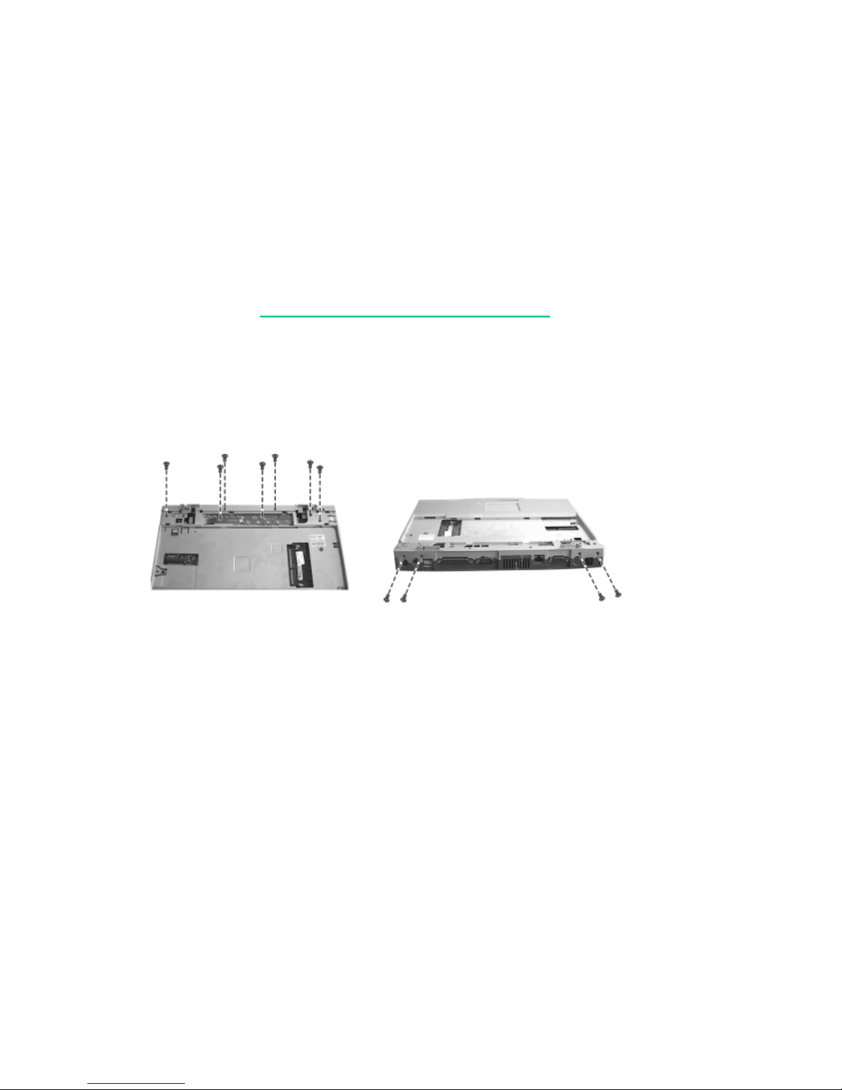
79
7521
7521
N/B MAINTENANCE
N/B MAINTENANCE
5.2.11 System Board
Disassembly
1. Remove the Keyboard. (See section 5.2.6 Disassembly.)
2. Remove the LCD assembly. (See section 5.2.8 Disassembly.)
3. Remove seven screws, and then take out the Easy Start board. (figure 5-21)
Figure 5-21 Figure 5-22
4. Remove four screws on the rear side of the notebook. (figure 5-22)
5. Remove the battery pack, heatsink, modem card, FDD/HDD module, and CD-ROM drive.
(See section 5.2.1 to 5.2.5 Disassembly.)
Page 81
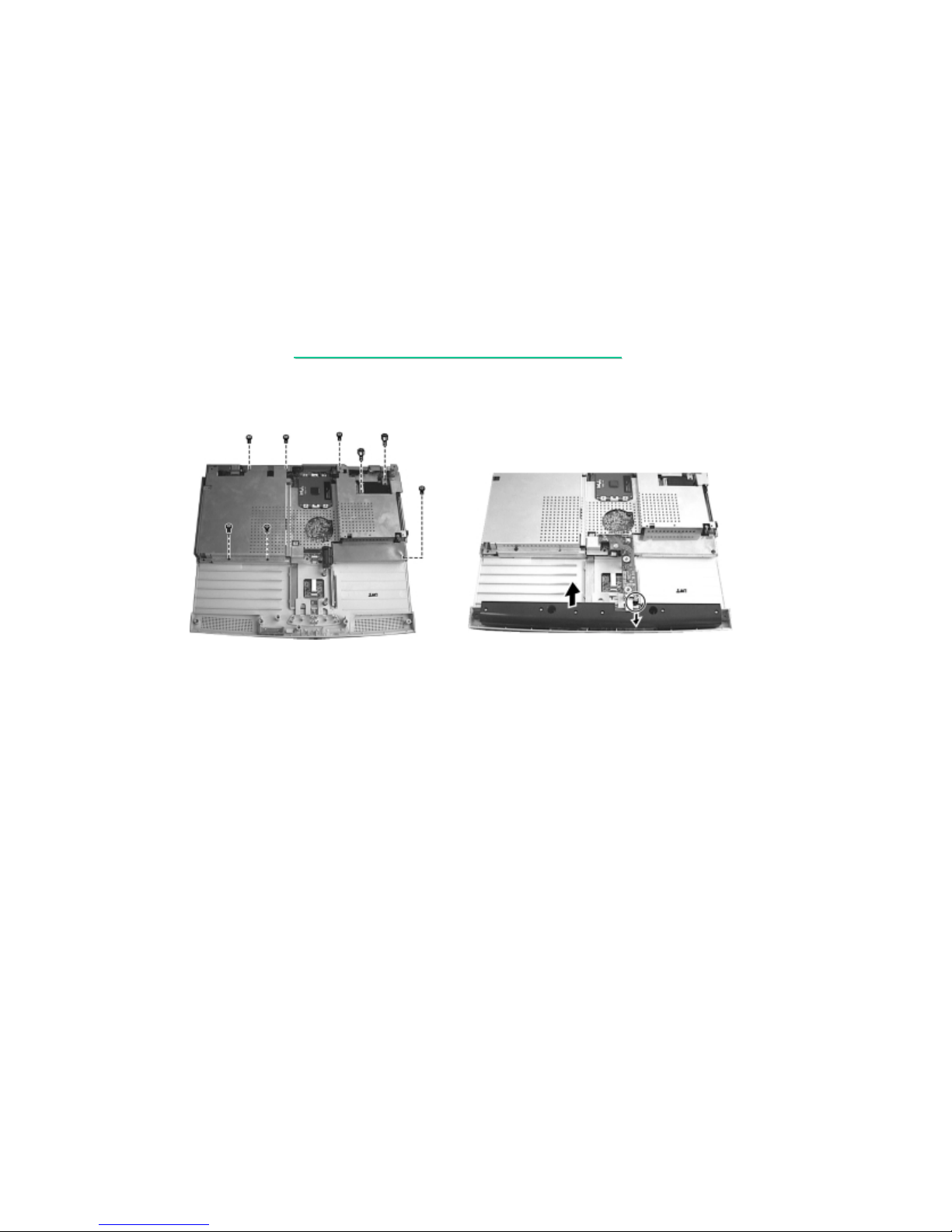
80
7521
7521
N/B MAINTENANCE
N/B MAINTENANCE
6. Remove six screws and two hexnut screws fastening the metal shield, and then lift the shield up
from the system board carefully. (figure 5-23)
Figure 5-23 Figure 5-24
7. Lift up the speaker assembly and disconnect the cable. (figure 5-24)
Page 82
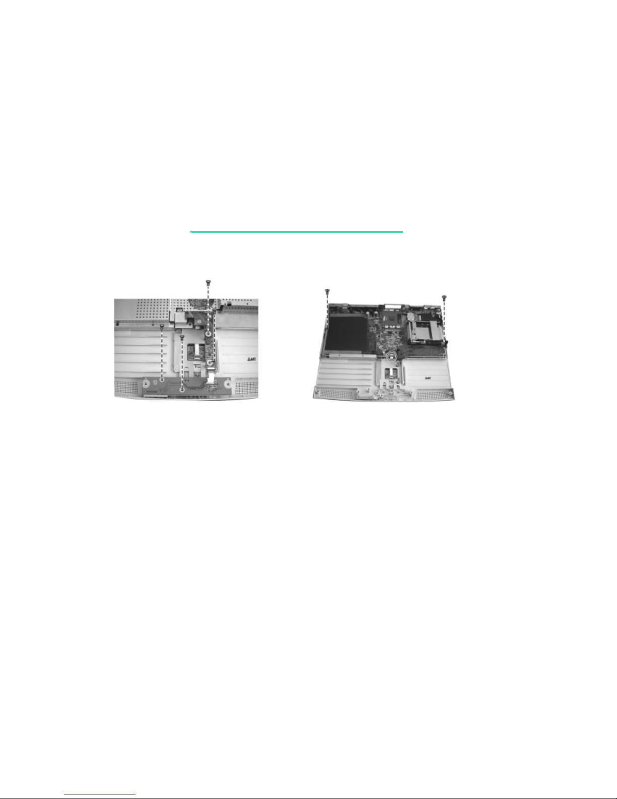
81
7521
7521
N/B MAINTENANCE
N/B MAINTENANCE
8. Remove four screws to take the recharge board apart. (figure 5-25)
Figure 5-25 Figure 5-26
9. Remove two screws fastening the system board and disconnect the cable of the touchpad.
Now you can lift the system board up from the base unit. (figure 5-26)
Reassembly
1. Fit the system board into place and secure with two screws.
2. Reconnect the touchpad’s cable.
3. Replace the metal shield and secure with six screws and two hexnut screws.
4. Replace the recharge board and secure with four screws.
5. Replace the speaker assembly and reconnect the cable.
Page 83

82
7521
7521
N/B MAINTENANCE
N/B MAINTENANCE
6. Replace the base unit frame and secure with twelve screws.
7. Replace the battery pack, heatsink, modem card, FDD/HDD module, and CD-ROM drive.
8. Secure the four screws on the rear side of the notebook.
9. Put the notebook back to the upright position. Replace the Easy Start board into the housing,
then secure with seven screws.
10. Replace the LCD assembly.
11. Replace the keyboard and Easy Start panel.
Page 84
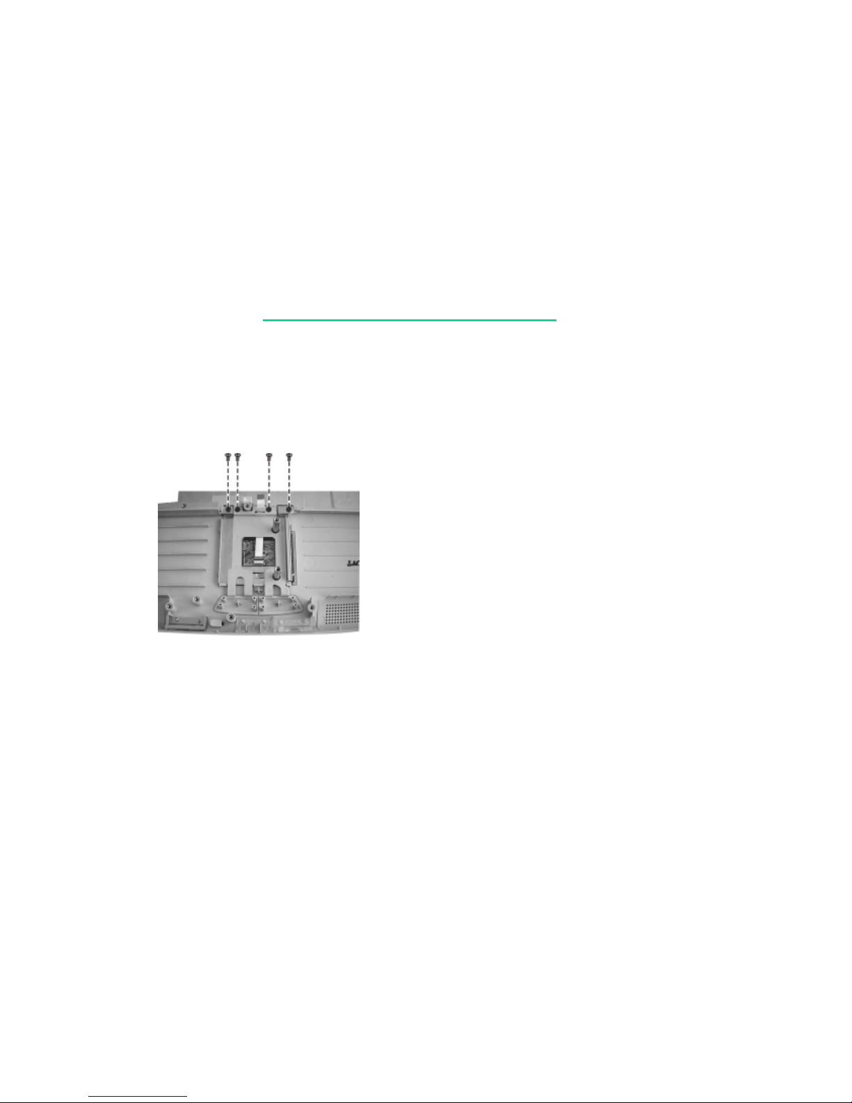
83
7521
7521
N/B MAINTENANCE
N/B MAINTENANCE
5.2.12 Touchpad
Disassembly
1. Remove the system board. (See section 5.2.11 Disassembly.)
2. Remove the four screws to lift up the touchpad holder and touchpad panel. (figure 5-27)
Figure 5-27
Reassembly
1. Replace the touchpad holder and touchpad panel, and secure with four screws.
2. Replace the system board and assemble the notebook. (See section 5.2.11 Reassembly.)
Page 85

84
7521
7521
N/B MAINTENANCE
N/B MAINTENANCE
6.1
6.1
Introduction
Introduction
Each time the computer is turned on, the system bios runs a seri
Each time the computer is turned on, the system bios runs a seri
es
es
of internal checks on the hardware. This power
of internal checks on the hardware. This power--
on self test (post) allows
on self test (post) allows
the computer to detect problems as early as the power
the computer to detect problems as early as the power--
on stage. Error
on stage. Error
messages of post can alert you to the problems of your computer.
messages of post can alert you to the problems of your computer.
If an error is detected during these tests, you will see
If an error is detected during these tests, you will see
an error
an error
message displayed on the screen. If the error occurs before the
message displayed on the screen. If the error occurs before the
display
display
is initialized,then the screen cannot display the error message.
is initialized,then the screen cannot display the error message.
Error
Error
codes or system beeps are used to identify a post error that occ
codes or system beeps are used to identify a post error that occ
urs
urs
when the screen is not available.
when the screen is not available.
The value for the diagnostic port
The value for the diagnostic port
(378H)
(378H)
is written at the beginning of
is written at the beginning of
the test. Therefore, if the test failed, the user can determine
the test. Therefore, if the test failed, the user can determine
where the
where the
problem occurred by reading the last value written to port
problem occurred by reading the last value written to port
378H
378H
by the
by the
378H
378H
port debug board plug at
port debug board plug at
PIO PORT.
PIO PORT.
6. Maintenance Diagnostics
Page 86
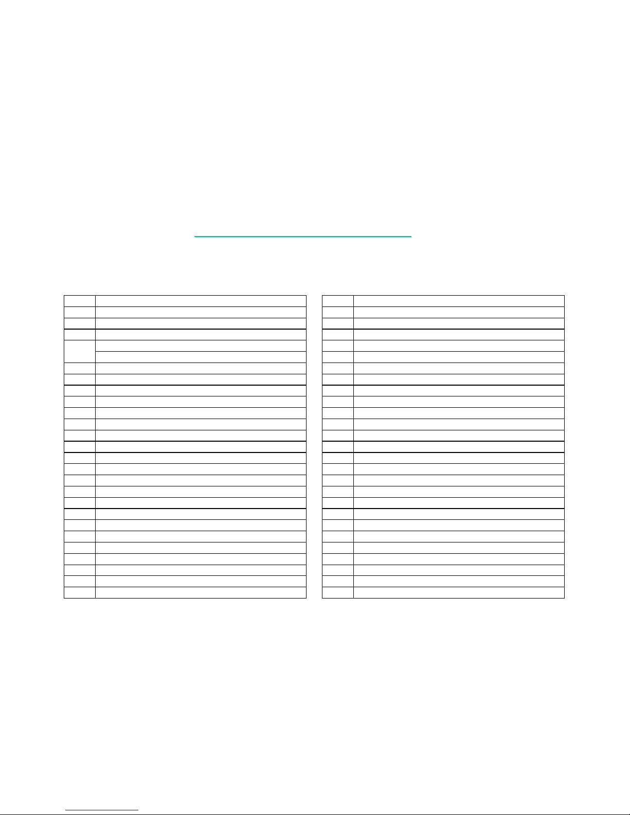
85
7521
7521
N/B MAINTENANCE
N/B MAINTENANCE
6. Maintenance Diagnostics
6.2 Error Codes : Following is a list of error codes in sequent display on the PIO debug board.
SYSTEM SOFT BIOS:
CODE DESCRIPTION
01h Start of boot loader sequence.
02h Initialize chipset.
03h Memory Sizing.
Perform conventional RAM(1st 640K) test with crossed-04h
pattern R/W
05h Move boot loader to the RAM.
06h Start point of execution of boot loader in RAM.
07h Shadow system BIOS.
08h Initialize clock synthesizer
09h Initialize audio controller.
0Ah Detect internal ISA MODEM
0Bh Proceed with normal boot
0Ch Proceed with crisis boot
0Fh DRAM sizing
10h Initial L1,L2 cache, make stack and diagnose CMOS.
11h Turn off fast A20 for post. Reset GDT's, 8259s quickly.
12h Signal power on reset at COMS.
13h Initialize the chipset, (SDRAM).
14h Search for ISA bus VGA adapter
15h Reset counter/timer 1, exite the RAM.
16h User register config through CMOS
18h Dispatch to 1st 64K RAM test
19h Checksum the ROM
1Ah Reset PIC's(8259s)
1Bh Initialize video adapter(s)
1Ch Initialize video (6845 regs)
CODE DESCRIPTION
1Dh Initialize color adapter
1Eh Initialize monochrome adapter
1Fh Test 8237A page registers
20h Perform keyboard self test
21h Test & initialize keyboard controller
22h Check if CMOS RAM valid
23h Test battery fail & CMOS X-SUM
24h Test the DMA controllers
25h Initialize 8237A controller
26h Initialize interrupt vectors table.
27h RAM quick sizing
28h Protected mode entered safely
29h RAM test completed
2Ah Protected mode exit successful
2Bh Setup shadow
2Ch Prepare to initialize video
2Dh Search for monochrome adapter
2Eh Search for color adapter, VGA initialize.
2Fh Signon messages displayed
30h Special init of keyboard ctlr
31h Test if keyboard present
32h Test keyboard interrupt
33h Test keyboard command Byte
34h Test, blank and count all RAM
35h Protected mode entered safely (2).
36h RAM test complete
Page 87

86
7521
7521
N/B MAINTENANCE
N/B MAINTENANCE
CODE DESCRIPTION
37h Protected mode exit successful
38h Update keyboard output port to disable gate of A20
39h Setup cache controller
3Ah Test if 18.2Hz periodic working
3Bh Initialize BIOS data area at 40:0.
3Ch Initialize the hardware interrupt vector tab l
3Dh Search and init the Mouse
3Eh Update num lock status
3Fh OEM initialization of COMM and LPT ports
40h Configure the COMM and LPT ports
41h Initialize the floppies
42h Initialize the hard disk
43h OEM's init of PM with USB
44h Initialize additional ROMs
45h Update NUMLOCK status
46h Test for coprocessor installed
47h OEM's init of power management, (check SMI)
48h OEM functions before boot (PCMCIA, CardBus)
49h Dispatch to operation system boot
4Ah Jump into bootstrap code
6. Maintenance Diagnostics
6.2 Error Codes : Following is a list of error codes in sequent display on the PIO debug board.
SYSTEM SOFT BIOS:
Page 88
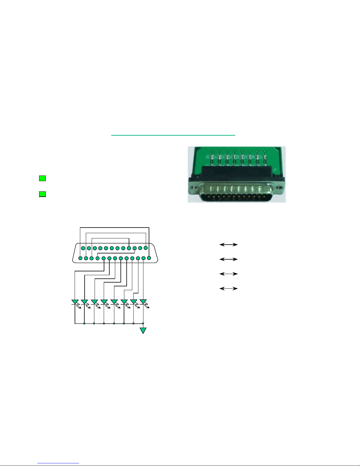
87
7521
7521
N/B MAINTENANCE
N/B MAINTENANCE
6. Maintenance Diagnostics
6.6.3.1
3.1
Diagnostic Tools :
Diagnostic Tools :
LED * 8
LED * 8
PIO CONNECTOR * 1
PIO CONNECTOR * 1
PIN1 : STROBE PIN 13 : SLCT
PIN1 : STROBE PIN 13 : SLCT
PIN10: ACK# PIN 16 : INT#
PIN10: ACK# PIN 16 : INT#
PIN11: BUSY PIN 17 : SELIN#
PIN11: BUSY PIN 17 : SELIN#
PIN12: PTERR PIN 14 : AUTOFD#
PIN12: PTERR PIN 14 : AUTOFD#
PIN{9:2}: PD{7:0}
PIN{9:2}: PD{7:0}
6.6.3.2
3.2
CIRCUIT:
CIRCUIT:
PIO
PIO
CONNECTOR
CONNECTOR
LED
LED
1
1
13
13
14
14
25
25
P/N:411904800001
DESCRIPTION :PWA;PWA-378PORT DEBUG BD
Note:Order it from MIC/TSSC
OR
Page 89

88
7521
7521
N/B MAINTENANCE
N/B MAINTENANCE
7. TROUBLE SHOOTING
7.1 NO POWER
7.2 NO DISPLAY
7.3 VGA CONTROLLER FAILURE LCD NO DISPLAY
7.4 EXTERNAL MONITOR NO DISPL AY
7.5 MEMORY TEST ERROR
7.6 KEYBOARD TEST ERROR OR TRACK PAD TEST ERROR
7.7 CD-ROM DRIVE TEST ERROR
7.8 HARD DRIVE TEST ERROR
7.9 USB PORT TEST ERROR
7.10 AUDIO FAILURE
7.11 SIO PORT TEST ERROR
7.12 PIO PORT TEST ERROR
7.13 PC-CARD SOKET FAIL
Page 90
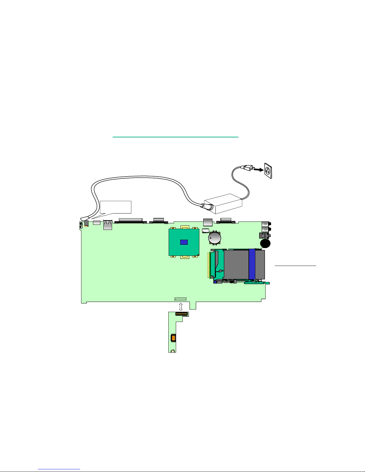
89
7521
7521
N/B MAINTENANCE
N/B MAINTENANCE
7.1 NO POWER:
When the power button is pressed, nothing happens ,power indicator does not light up.
Power Jack
22.5V 2.67A
1. Check AC Adaptor.
2. Check OUTLET.
3.Check Charge B’D
OUTLET
MOTHER BOARD
Charge B’D
J514
J1
Page 91
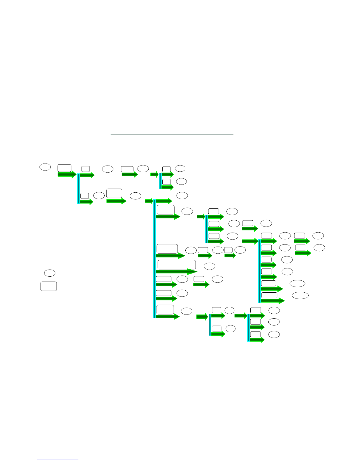
90
7521
7521
N/B MAINTENANCE
N/B MAINTENANCE
POWER IN
P25
PJ501
PL1, PF1
PD2
PWR_VDDIN
P25
VDD5
P23
F5, U32 Q26
+S5V
Q27
VDD5S
P23
P23
PU1
ADINP
P26
P25
PD1, PD3,
PL4
D/VMAIN
VMAIN
P29
PQ502
PQ503,PU9
+S3V_P
P27
JO4
+S3V
P29
PQ10
S1.8V
P29
PQ504
+3V
P29
JO6
+S1.8V
P29
PU13,PU4
1.8V
P28
PQ14
2.5V
P29
JO9
+2.5V
P29
+S12V
PU9,PQ7,PQ9
PL502,PU501
P27
PU9,PQ7
PQ9,PL502
+S5V_P
P27
PQ3
+5V
P29
J01
+S5V
P29
PQ501
+12V
P29
PL5,PU14,PU5,PU6,PU7
PU10,PU11,PU12,
P30
VCC_CORD
7.1 NO POWER:
When the power button is pressed, nothing happens ,power indicator does not light up.
PU13,PU3
1.5V
P28
JO11
+1.8V
P29
P29
:Page 29 on circuit diagram.
PD1, PD3,
PL4
:Through by parts PD1,PD3,PL4.
Note:
L25
ICVCC
P5
L23
LVDSVCC
P5
L11
PLLVCC
P5
L532
DACAVDD
P5
L54,R214
DCLKAVDD
P5
L55,R223
ECLKAVDD
P5
U4
VA
P29
JS15
+5VS_FDD
P13
JS14
+5VS_HDD
P13
JS501
+5VS_CDROM
P13
Page 92
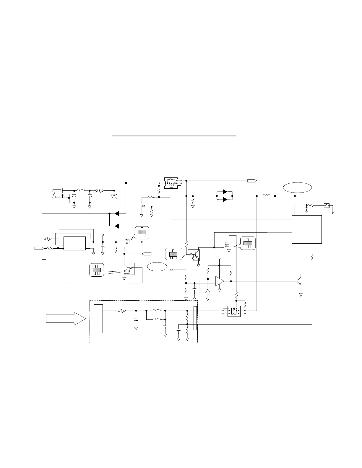
91
7521
7521
N/B MAINTENANCE
N/B MAINTENANCE
Symptom:
Symptom:
When the power button is pressed, nothing happens, no fan activi
When the power button is pressed, nothing happens, no fan activi
ty is heard and power indicator is not light up
ty is heard and power indicator is not light up..
D/VMAIN
PF1
6.5A/32VDC
U12
H8
ADINP
PJ501
PC4
0.1U
PD502
RLZ24D
PD3
EC31QS04
PL4
120Z/100M
PR14
226K
PQ6
DTC144WK
2
3
1
PQ12
2N7002
G
D
S
3
12
D
SG
IN 5VTAP
SENSE OUT
F/B ERRSHUTDN GND
PWR_VDDIN
SW_VDD5
FROM H8
VDD5
SGD
SW_VDD5#
+5V
F5
R233
0
U32
LP2951-02BM
8
2
7
3
6
1
5
4
X
C235
4.7U
Q26
Q25
DTC144WK
3
2
1
D
SG
3
12
ADEN#_P
BATT
1
4
5
6
7
8
2
3
PJ4
6
PF1
6.5A/32VDC
PR2
301K
PC5
0.1U
50V
PR1
100K
PU8
SI4435DY
PR21
33K
PR20
100K
BAT_V
BATTERY IN
RP22
38
BAT_V
POWER IN
PL1
120Z/100M
D
S
G
LEARNING
PR10
1M
PQ5
2N7002
PR11
120K
G
4
6
7
8
2
3
S
D
1
5
PR12
470K
PR18
715K
PR17
100K
+
-
PC6
0.1U
PL1
120Z/100M
PL2
120Z/100M
PC1
0.01U
PC17
0.1U
PQ8
PR13
10K
PR15
100K
VDD5S_P
Q508
BATT_ALARM
7.1 NO POWER:
PU1
SI4835DY
PC3
0.1U
PR89
4.7K
PD1
EC31QS04
PD2
EC10QS041M
PD4
EC10QS041M
D/VMAIN
1.25V
PU2B
J514
CHARGE B’D
POWERBTN#
SW2
POWER BUTTON
R577
C577
R230
100K
J1
47
Page 93
92
7521
7521
N/B MAINTENANCE
N/B MAINTENANCE
Symptom:
Symptom:
When the power button is pressed, nothing happens, no fan activi
When the power button is pressed, nothing happens, no fan activi
ty is heard and power indicator is not light up
ty is heard and power indicator is not light up..
7.1 NO POWER:
No power
Is the
notebook
power source O.K?
(Either AC adapter
or battery)
No
Connect
AC adapter
or battery
Yes
Try another known good battery,
charger board or AC adapter.
Power
O.K ?
Replace motherboard
or go into board level
troubleshooting
Replace the faulty
battery, charger
board or AC adapter.
Board level
troubleshooting
for no power
Next Page
1. Check the power source
from battery circuit.
From mother board J514
check the following signal & parts.
SIGNAL: PARTS:
Yes
No
PU8
PR20
PR21
PQ12
J514
CHARGE B’D
BATT
BAT_V
WHERE
FROM POWER SOURCE
PROBLEM
?
AC-ADAPTOR
BATTERY PACK
Page 94
93
7521
7521
N/B MAINTENANCE
N/B MAINTENANCE
Symptom:
Symptom:
When the power button is pressed, nothing happens, no fan activi
When the power button is pressed, nothing happens, no fan activi
ty is heard and power indicator is not light up
ty is heard and power indicator is not light up..
7.1 NO POWER:
CONTINUE
2. Check the power source
from AC adapter. (PJ501)
POWER
OK?
END
NO
YES
If “D/VMAIN”
failure.
If “VCC_CORE”
(CPUVCC)
failure.
If “+S12V, +S5V_P
or +S3V_P” failure.
If “1.5V, 1.8V”
Failure.
If “VDD5”
failure.
CHECK: PD1,PD3,PL4,PC16,PR20,PR21
PQ12,PU8,PC15,PC33…….
CHECK: PL5,PU14,PU5,PU10,PU6,PU11,
PU7,PU12,PD7,PL8,PR29,PR44,
PC50,PC49,PC48,PC47,PC46….
CHECK : PU9,PQ7,PQ9,PL502,PD501
PU501,PR4,PQ502,PQ503,
PL501,PR2,PD6,PD505…….
CHECK: PU13,PU3,PU4,PD9,PD10,PD5
PD6,PL6,PL10,PR30,PR34….
CHECK : PD2,PD4,F5,U32,C235......
PL1
PF1
PC3
PC4 PR12 PR14
PD502 PR11 PD1
PU1 PR10 ……..
SIGNAL: PARTS:
ADINP
LEARING
Page 95
94
7521
7521
N/B MAINTENANCE
N/B MAINTENANCE
7.2 NO DISPLAY
There is no display on both LCD and monitor
NO DISPLAY
YES
Connect the I/O device
& cables to the system
one at a time to find out
the faulty parts then
replace and end.
Replace motherboard or into
board-level
Troubleshooting.
Plug PIO debug board to PIO
port and get the 378h error code.
Is there
any error code
shown on debug
board ?
Check system clock or reset
circuit and major chip for any
cold solder.
NO
Refer to the error
code description
and find out the
error.
YES
1. Check if power system is O.K .
2. Remove all the I/O device
from system.
YES
NO
Reboot
and display
OK?
Check switch setting or
replace a known good
battery.
NO
Reboot
and display
OK?
Replace the faulty
parts then end.
Page 96
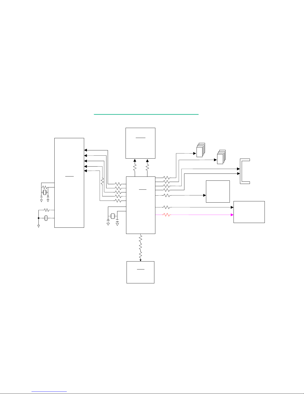
95
7521
7521
N/B MAINTENANCE
N/B MAINTENANCE
7.2 NO DISPLAY
******System Clock Check ******
U503
CPU
FC-PGA
U13
Clock
Generator
ICS9248-102
R90
HCLK_CPU
R104
APICCLK
45
48
W37
J33
C151
U22
SIS 630
U27
Super I/O
PC97338VJG
46
R89
R136
R139
R98
9
17
26
14.318MHz
X4
C158
4
5
CPUCLK
630PCLK
CLK14_VGA
USB_48MHZ
5
20 R140
21 R141
28 R92
29 R91
SDRAMCLK2
SDRAMCLK3
A18
AJ14
AJ15
J1
25
R144
2
630SDCLK
AG1
R99
IO_48MHZ
32.768K
H1
H2
C597
C606
R596
X501
X3
R113
B5
A5
25M
SDRAMCLK0
SDRAMCLK1
J6
U16 U21
U26 U30
U15 U20
U25 U29
U505
TI1225
PCMCIA
CONTROLLER
11 R137
PCLKCARD
180
U31
LPC TO ISA
W83626F
12 R138
LPC2ISACLK
21
ISA 14M
26
48 R105
R94
R236
R93
SODIMM
Page 97
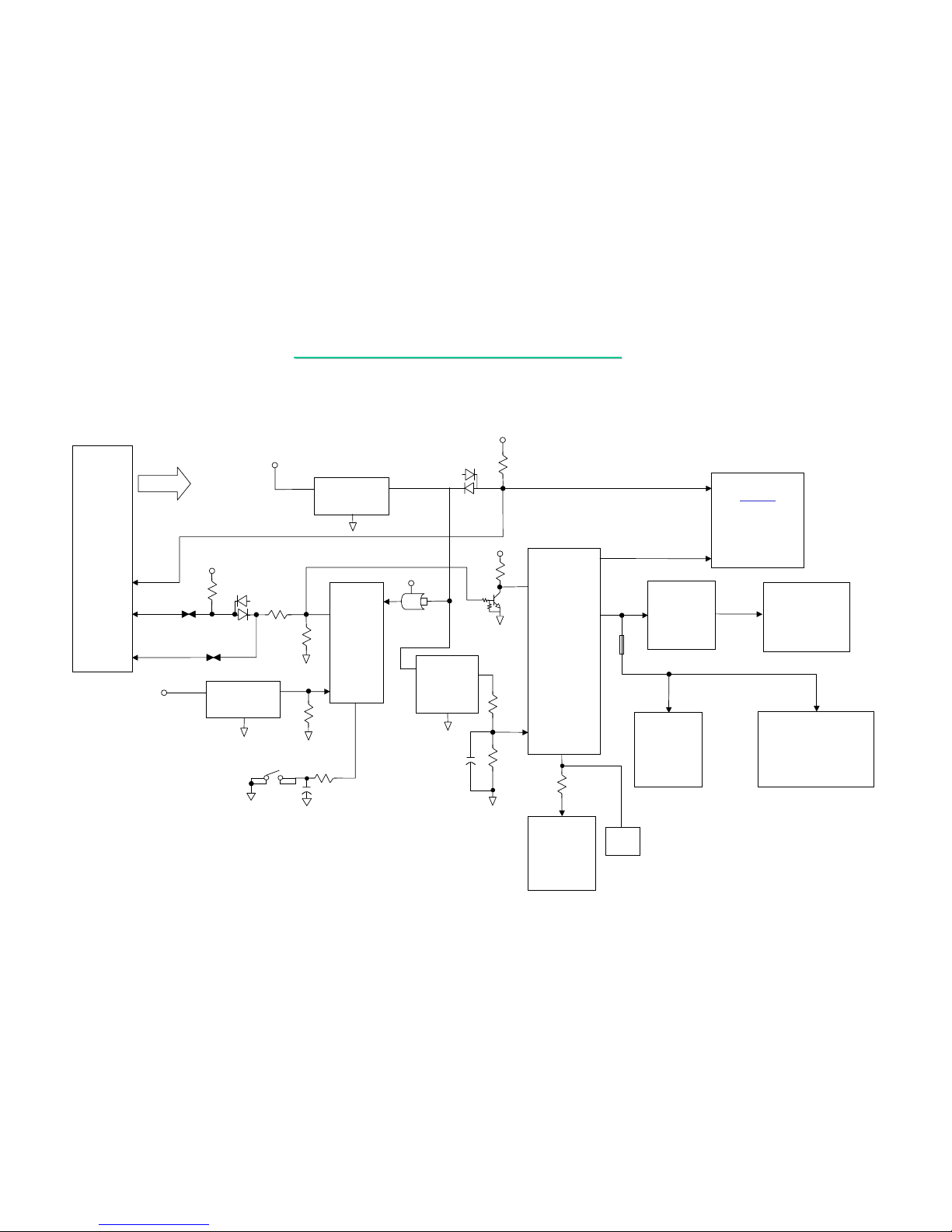
96
7521
7521
N/B MAINTENANCE
N/B MAINTENANCE
U9
MAX809
VCC
RESET#
GND
U22
SIS
630
U12
H8
PWROK
POWER ON BTN
U503
CPU
FC-PGA
CPU_PWRGOOD
H8_PWRON
PWR_ON
CPU_PWR_ON
D/CPU_PWR_ON
D/PWR_ON
+S12V
+S5V_P
+3V_P
1.5V
1.8V
VCC_CORE
2.5V
D7
R85
R132
R133
D11
R84
+3V
+3V
+5V
U18
CPURST#
18
14
U31
LPC
TO
ISA
14
PCIRST#
U27
Super I/O
PC97338VJG
RSTDRY
77 100
U505
PCMCIA/CARDBUS
CONTROLLER
TI 1225
JL21
PCIRSTNS#
166
U17
POWER
SWITCH
MATRIX
14
U5
CODEC
CS4299
11
U504
MAX809
VCC
RESET#
GND
VDD5
H8_RESET#
R57
ARST
23
R577
SW2
POWERBTN#
R570
7521
Power
Module
7.2 NO DISPLAY
******Power Good & Reset System ******
U14
MAX809
VCC
RESET#
GND
SIS PWROK
R126
R146
SIS_PWRBTN#
Q11
R606
+S3V
C577
1000P
C174
J511
FM/D
Page 98
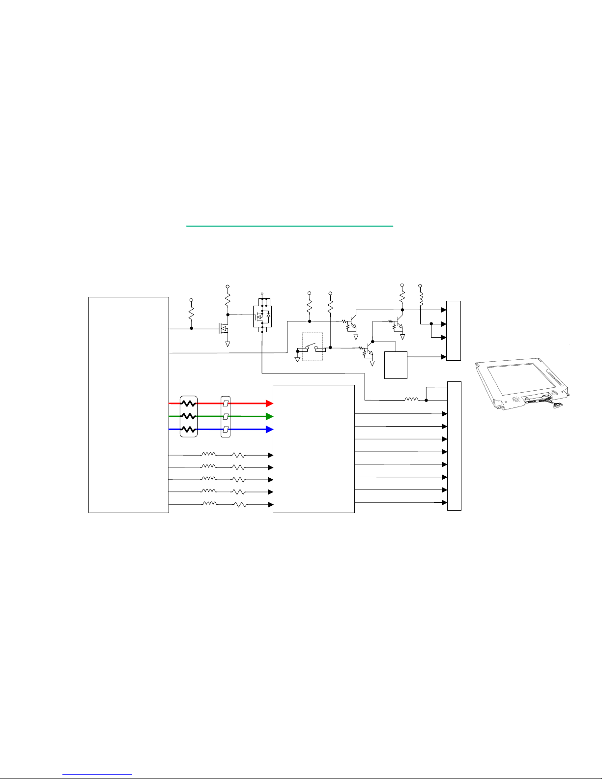
97
7521
7521
N/B MAINTENANCE
N/B MAINTENANCE
U22
SIS 630
U2
DS90C363MTD
R[2~7]_301
G[2~7]_301
B[2~7]_301
FA6,FA8,FA10
FA7,FA9,FA11
RP7,RP9,RP11
RP8,RP10,RP12
VBHSYNC
VBVSYNC
VBBLANK#
VGCLK
L528
L51
L529
L531
R526
R18
R11
R525
22
23
25
26
TXCLKOUT+
TXCLKOUT-
TXOUT0+
TXOUT0-
TXOUT1+
TXOUT1-
TXOUT2+
TXOUT2-
32
33
40
41
38
39
34
35
27
VBCLK
7
11
16
20
8
12
15
19
1 23
5 678
4
S
G
D
1
2
D
S
G
FPVCC
R5
+5V
+12V
R8
Q3
+3V
Q4
L4
ENABKL_VGA#
SW1
ENABKL_VGA
U12
H8
BLADJ
4
45
1
LID_OPEN#
24
LCD
+5V
L15
2
3
J1
+3V
R190
Q16
Q20
Q5
+3V
+3V
R19
R196
7.3. VGA CONTROLLER FAILURE LCD NO DISPLAY
There is no display or picture abnormal on LCD.
J2
LCD COVER SW
L537 R623
Page 99
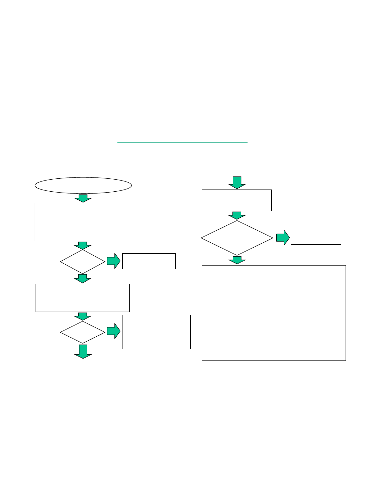
98
7521
7521
N/B MAINTENANCE
N/B MAINTENANCE
VGA CONTROLLER FAILURE
1. Confirm LCD panel or monitor is good
and check the cable are connected
properly.
2. Try another known good monitor or
LCD module.
Display
OK?
Remove all the I/O device & cable from
motherboard except LCD panel or extended
monitor.
Display
OK?
Replace faulty
LCD or monitor.
Connect the I/O device & cable
to the M/B one at a time to find
out which part is causing the
problem.
YES
NO
YES
NO
Replace motherboard
or into board-level
Troubleshooting.
YES
Re-soldering.
NO
One of the following parts on the mother-board may be
defective, use an oscilloscope to check the following signal or
replace the parts one at a time and test after each replacement.
Parts:
U22 U2
U12 J1
J2 Q20
Q16 Q5
Q4 Q3
SW1 R19
R190 R196
L4 R8
R5 L25
L23 L11
Signals:
TXCLKOUTTXCLKOUT+
TXOUT0TXOUT0+
TXOUT1TXOUT1+
TXOUT2TXOUT2+
Check if
U22, U2, J1, J2
are cold
solder?
R[2~7]301
G[2~7]301
B[2~7]301
VBHSYNC
VBVSYNC
VBBLANK#
VGCLK
FPVCC
LID_OPEN#
FA8 FA9
FA11 FA10
FA6 FA7
RP11 RP12
RP10 RP9
RP8 RP7
L528 L51
L529 L531
R528 RR18
R11 R525
7.3. VGA CONTROLLER FAILURE LCD NO DISPLAY
There is no display or picture abnormal on LCD.
Page 100
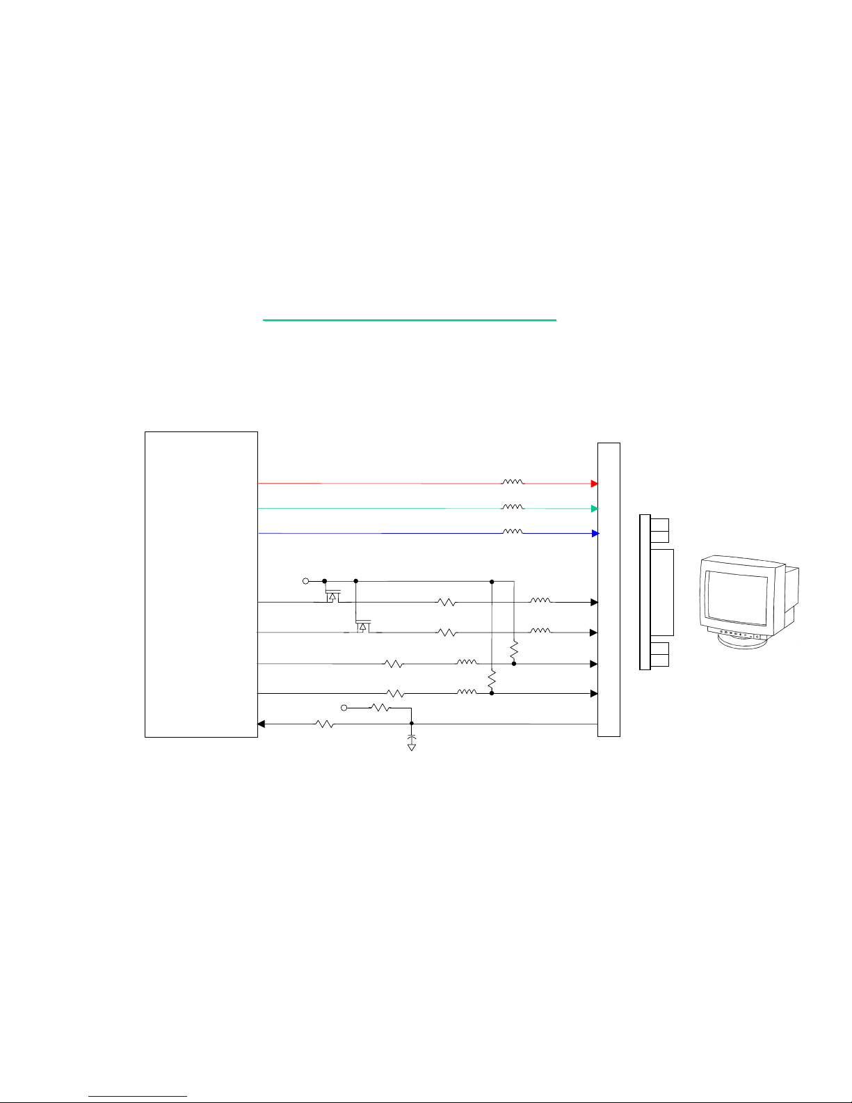
99
7521
7521
N/B MAINTENANCE
N/B MAINTENANCE
U22
SIS 630
G
D
S
G
D
S
RED
GREEN
BLUE
HSYNC
VSYNC
DDDA
DDCK
Q23
Q22
L514
L511
L510
L509
L515
L513
L508
+5V
R256
R261
+3V
R518R516CRT_IN#
J506
1
2
3
13
14
12
15
10
7.4 EXTERNAL MONITOR NO DISPLAY
There is no display or picture abnormal on CRT monitor.
CRT MONITOR
C504
R621
0
R620
R205
R206
 Loading...