

Page 1

Programming the MIPS32® 74K™ Core
Family
Document Number: MD00541
Revision 02.14
March 30, 2011
Page 2

Unpublished rights (if any) reserved under the copyright laws of the United States of America and other countries.
This document contains information that is proprietary to MIPS Tech, LLC, a Wave Computing company (“MIPS”) and MIPS’
affiliates as applicable. Any copying, reproducing, modifying or use of this information (in whole or in part) that is not expressly
permitted in writing by MIPS or MIPS’ affiliates as applicable or an authorized third party is strictly prohibited. At a minimum,
this information is protected under unfair competition and copyright laws. Violations thereof may result in criminal penalties
and fines. Any document provided in source format (i.e., in a modifiable form such as in FrameMaker or Microsoft Word
format) is subject to use and distribution restrictions that are independent of and supplemental to any and all confidentiality
restrictions. UNDER NO CIRCUMSTANCES MAY A DOCUMENT PROVIDED IN SOURCE FORMAT BE DISTRIBUTED TO A THIRD
PARTY IN SOURCE FORMAT WITHOUT THE EXPRESS WRITTEN PERMISSION OF MIPS (AND MIPS’ AFFILIATES AS APPLICABLE)
reserve the right to change the information contained in this document to improve function, design or otherwise.
MIPS and MIPS’ affiliates do not assume any liability arising out of the application or use of this information, or of any error or
omission in such information. Any warranties, whether express, statutory, implied or otherwise, including but not limited to the
implied warranties of merchantability or fitness for a particular purpose, are excluded. Except as expressly provided in any
written license agreement from MIPS or an authorized third party, the furnishing of this document does not give recipient any
license to any intellectual property rights, including any patent rights, that cover the information in this document.
The information contained in this document shall not be exported, reexported, transferred, or released, directly or indirectly, in
violation of the law of any country or international law, regulation, treaty, Executive Order, statute, amendments or
supplements thereto. Should a conflict arise regarding the export, reexport, transfer, or release of the information contained in
this document, the laws of the United States of America shall be the governing law.
The information contained in this document constitutes one or more of the following: commercial computer software,
commercial computer software documentation or other commercial items. If the user of this information, or any related
documentation of any kind, including related technical data or manuals, is an agency, department, or other entity of the United
States government ("Government"), the use, duplication, reproduction, release, modification, disclosure, or transfer of this
information, or any related documentation of any kind, is restricted in accordance with Federal Acquisition Regulation 12.212
for civilian agencies and Defense Federal Acquisition Regulation Supplement 227.7202 for military agencies. The use of this
information by the Government is further restricted in accordance with the terms of the license agreement(s) and/or applicable
contract terms and conditions covering this information from MIPS Technologies or an authorized third party.
MIPS, MIPS I, MIPS II, MIPS III, MIPS IV, MIPS V, MIPSr3, MIPS32, MIPS64, microMIPS32, microMIPS64, MIPS-3D, MIPS16,
MIPS16e, MIPS-Based, MIPSsim, MIPSpro, MIPS-VERIFIED, Aptiv logo, microAptiv logo, interAptiv logo, microMIPS logo, MIPS
Technologies logo, MIPS-VERIFIED logo, proAptiv logo, 4K, 4Kc, 4Km, 4Kp, 4KE, 4KEc, 4KEm, 4KEp, 4KS, 4KSc, 4KSd, M4K, M14K,
5K, 5Kc, 5Kf, 24K, 24Kc, 24Kf, 24KE, 24KEc, 24KEf, 34K, 34Kc, 34Kf, 74K, 74Kc, 74Kf, 1004K, 1004Kc, 1004Kf, 1074K, 1074Kc,
1074Kf, R3000, R4000, R5000, Aptiv, ASMACRO, Atlas, "At the core of the user experience.", BusBridge, Bus Navigator, CLAM,
CorExtend, CoreFPGA, CoreLV, EC, FPGA View, FS2, FS2 FIRST SILICON SOLUTIONS logo, FS2 NAVIGATOR, HyperDebug,
HyperJTAG, IASim, iFlowtrace, interAptiv, JALGO, Logic Navigator, Malta, MDMX, MED, MGB, microAptiv, microMIPS, Navigator,
OCI, PDtrace, the Pipeline, proAptiv, Pro Series, SEAD-3, SmartMIPS, SOC-it, and YAMON are trademarks or registered
trademarks of MIPS and MIPS’ affiliates as applicable in the United States and other countries.
All other trademarks referred to herein are the property of their respective owners.
WƌŽŐƌĂŵŵŝŶŐ ƚŚĞ D/W^ϯϮΠ ϳϰ<Ρ ŽƌĞ &ĂŵŝůLJ ZĞǀŝƐŝŽŶ ϬϮϭϰ
Page 3

Table of Contents
Chapter 1: Introduction........................................................................................................................11
1.1: Chapters of this manual............................................................................................................................. 12
1.2: Conventions............................................................................................................................................... 12
1.3: 74K™ core features................................................................................................................................... 13
1.4: A brief guide to the 74K™ core implementation ........................................................................................ 14
1.4.1: Notes on pipeline overview diagram (Figure 1.1):............................................................................ 14
1.4.2: Branches and branch delays............................................................................................................17
1.4.3: Loads and load-to-use delays.......................................................................................................... 18
1.4.4: Queues, Resource limits and Consequences.................................................................................. 19
Chapter 2: Initialization and identity...................................................................................................21
2.1: Probing your CPU - Config CP0 registers.................................................................................................21
2.1.1: The Config register........................................................................................................................... 22
2.1.2: The Config1-2 registers.................................................................................................................... 23
2.1.3: The Config3 register......................................................................................................................... 24
2.1.4: The Config6 register......................................................................................................................... 25
2.1.5: CPU-specific configuration — Config7.............................................................................................26
2.2: PRId register — identifying your CPU type ............................................................................................... 26
Chapter 3: Memory map, caching, reads, writes and translation ....................................................29
3.1: The memory map ...................................................................................................................................... 29
3.2: Fixed mapping option................................................................................................................................30
3.3: Reads, writes and synchronization............................................................................................................ 30
3.3.1: Read/write ordering and cache/memory data queues in the 74K™ core......................................... 30
3.3.2: The “sync” instruction in 74K™ family cores....................................................................................31
3.3.3: Write gathering and “write buffer flushing” in 74K™ family cores..................................................... 32
3.4: Caches ...................................................................................................................................................... 32
3.4.1: The L2 cache option.........................................................................................................................32
3.4.2: Cacheability options......................................................................................................................... 33
3.4.3: Uncached accelerated writes........................................................................................................... 34
3.4.4: The cache instruction and software cache management.................................................................34
3.4.5: Cache instructions and CP0 cache tag/data registers.....................................................................35
3.4.6: L1 Cache instruction timing..............................................................................................................37
3.4.7: L2 cache instruction timing............................................................................................................... 37
3.4.8: Cache management when writing instructions - the “synci” instruction ........................................... 37
3.4.9: Cache aliases...................................................................................................................................38
3.4.10: Cache locking.................................................................................................................................39
3.4.11: Cache initialization and tag/data registers ..................................................................................... 39
3.4.12: L23TagLo Regiser..........................................................................................................................40
3.4.13: L23DataLo Register.......................................................................................................................40
3.4.14: L23DataHi Register........................................................................................................................40
3.4.15: TagLo registers in special modes .................................................................................................. 41
3.4.16: Parity error exception handling and the CacheErr register............................................................41
3.4.17: ErrCtl register................................................................................................................................. 42
3.5: Bus error exception ................................................................................................................................... 43
3.6: Scratchpad memory/SPRAM..................................................................................................................... 44
3.7: Common Device Memory Map..................................................................................................................46
3 Programming the MIPS32® 74K™ Core Family, Revision 02.14
Page 4

3.8: The TLB and translation............................................................................................................................47
3.8.1: A TLB entry......................................................................................................................................47
3.8.2: Live translation and micro-TLBs....................................................................................................... 48
3.8.3: Reading and writing TLB entries: Index, Random and Wired..........................................................48
3.8.4: Reading and writing TLB entries - EntryLo0-1, EntryHi and PageMask registers............................ 49
3.8.5: TLB initialization and duplicate entries.............................................................................................50
3.8.6: TLB exception handlers — BadVaddr, Context, and ContextConfig registers.................................51
Chapter 4: Programming the 74K™ core in user mode....................................................................55
4.1: User-mode accessible “Hardware registers”.............................................................................................55
4.2: Prefetching data ........................................................................................................................................ 56
4.3: Using “synci” when writing instructions...................................................................................................... 56
4.4: The multiplier.............................................................................................................................................57
4.5: Tuning software for the 74K™ family pipeline ........................................................................................... 58
4.5.1: Cache delays and mitigating their effect..........................................................................................58
4.5.2: Branch delay slot..............................................................................................................................59
4.6: Tuning floating-point..................................................................................................................................59
4.7: Branch misprediction delays...................................................................................................................... 60
4.8: Load delayed by (unrelated) recent store.................................................................................................. 60
4.9: Minimum load-miss penalty.......................................................................................................................60
4.10: Data dependency delays.........................................................................................................................61
4.10.1: More complicated dependencies ................................................................................................... 64
4.11: Advice on tuning instruction sequences (particularly DSP).....................................................................65
4.12: Multiply/divide unit and timings................................................................................................................ 65
Chapter 5: Kernel-mode (OS) programming and Release 2 of the MIPS32® Architecture............67
5.1: Hazard barrier instructions ........................................................................................................................ 67
5.2: MIPS32® Architecture Release 2 - enhanced interrupt system(s)............................................................ 68
5.2.1: Traditional MIPS® interrupt signalling and priority........................................................................... 69
5.2.2: VI mode - multiple entry points, interrupt signalling and priority.......................................................70
5.2.3: External Interrupt Controller (EIC) mode.......................................................................................... 70
5.3: Exception Entry Points .............................................................................................................................. 71
5.3.1: Summary of exception entry points..................................................................................................72
5.4: Shadow registers....................................................................................................................................... 73
5.5: Saving Power ............................................................................................................................................ 75
5.6: The HWREna register - Control user rdhwr access .................................................................................. 75
Chapter 6: Floating point unit..............................................................................................................77
6.1: Data representation...................................................................................................................................77
6.2: Basic instruction set................................................................................................................................... 78
6.3: Floating point loads and stores.................................................................................................................. 79
6.4: Setting up the FPU and the FPU control registers .................................................................................... 79
6.4.1: IEEE options .................................................................................................................................... 79
6.4.2: FPU “unimplemented” exceptions (and how to avoid them)............................................................79
6.4.3: FPU control register maps ............................................................................................................... 80
6.5: FPU pipeline and instruction timing...........................................................................................................82
6.5.1: FPU register dependency delays..................................................................................................... 84
6.5.2: Delays caused by long-latency instructions looping in the M1 stage............................................... 84
6.5.3: Delays on FP load and store instructions......................................................................................... 84
6.5.4: Delays when main pipeline waits for FPU to decide not to take an exception................................. 84
6.5.5: Delays when main pipeline waits for FPU to accept an instruction..................................................85
6.5.6: Delays on mfc1/mtc1 instructions .................................................................................................... 85
Programming the MIPS32® 74K™ Core Family, Revision 02.14 4
Page 5

6.5.7: Delays caused by dependency on FPU status register fields.......................................................... 85
6.5.8: Slower operation in MIPS I™ compatibility mode............................................................................85
Chapter 7: The MIPS32® DSP ASE .....................................................................................................87
7.1: Features provided by the MIPS® DSP ASE..............................................................................................87
7.2: The DSP ASE control register...................................................................................................................88
7.2.1: DSP accumulators ........................................................................................................................... 89
7.3: Software detection of the DSP ASE..........................................................................................................89
7.4: DSP instructions........................................................................................................................................90
7.4.1: Hints in instruction names................................................................................................................ 90
7.4.2: Arithmetic - 64-bit............................................................................................................................. 91
7.4.3: Arithmetic - saturating and/or SIMD Types......................................................................................91
7.4.4: Bit-shifts - saturating and/or SIMD types.......................................................................................... 91
7.4.5: Comparison and “conditional-move” operations on SIMD types......................................................91
7.4.6: Conversions to and from SIMD types .............................................................................................. 92
7.4.7: Multiplication - SIMD types with result in GP register ...................................................................... 92
7.4.8: Multiply Q15s from paired-half and accumulate...............................................................................93
7.4.9: Load with register + register address............................................................................................... 93
7.4.10: DSPControl register access........................................................................................................... 93
7.4.11: Accumulator access instructions....................................................................................................94
7.4.12: Dot products and building blocks for complex multiplication..........................................................94
7.4.13: Other DSP ASE instructions .......................................................................................................... 95
7.5: Macros and typedefs for DSP instructions ................................................................................................ 95
7.6: Almost Alphabetically-ordered table of DSP ASE instructions..................................................................96
7.7: DSP ASE instruction timing.....................................................................................................................100
Chapter 8: 74K™ core features for debug and profiling.................................................................102
8.1: EJTAG on-chip debug unit ...................................................................................................................... 102
8.1.1: Debug communications through JTAG..........................................................................................103
8.1.2: Debug mode...................................................................................................................................103
8.1.3: Exceptions in debug mode.............................................................................................................104
8.1.4: Single-stepping .............................................................................................................................. 104
8.1.5: The “dseg” memory decode region................................................................................................ 104
8.1.6: EJTAG CP0 registers, particularly Debug......................................................................................106
8.1.7: The DCR (debug control) memory-mapped register......................................................................108
8.1.8: The DebugVectorAddr memory-mapped register..........................................................................110
8.1.9: JTAG-accessible registers.............................................................................................................110
8.1.10: Fast Debug Channel....................................................................................................................112
8.1.11: EJTAG breakpoint registers......................................................................................................... 115
8.1.12: Understanding breakpoint conditions...........................................................................................117
8.1.13: Imprecise debug breaks...............................................................................................................118
8.1.14: PC Sampling with EJTAG............................................................................................................118
8.1.15: JTAG-accessible and memory-mapped PDtrace TCB Registers ................................................ 119
8.2: PDtrace™ instruction trace facility........................................................................................................... 121
8.2.1: 74K core-specific fields in PDtrace™ JTAG-accessible registers..................................................121
8.2.2: CP0 registers for the PDtrace™ logic............................................................................................123
8.2.3: JTAG triggers and local control through TraceIBPC/TraceDBPC..................................................125
8.2.4: UserTraceData1 reg and UserTraceData2 reg.............................................................................. 126
8.2.5: Summary of when trace happens .................................................................................................. 126
8.3: CP0 Watchpoints..................................................................................................................................... 128
8.3.1: The WatchLo0-3 registers..............................................................................................................128
8.3.2: The WatchHi0-3 registers .............................................................................................................. 128
8.4: Performance counters.............................................................................................................................129
5 Programming the MIPS32® 74K™ Core Family, Revision 02.14
Page 6

8.4.1: Reading the event table.................................................................................................................130
Appendix A: References ....................................................................................................................135
Appendix B: CP0 register summary and reference.........................................................................137
B.1: Miscellaneous CP0 register descriptions................................................................................................140
B.1.1: Status register................................................................................................................................141
B.1.2: The UserLocal register .................................................................................................................. 143
B.1.3: Exception control: Cause and EPC registers................................................................................. 143
B.1.3.1: The Cause register............................................................................................................... 143
B.1.4: The EPC register...........................................................................................................................145
B.1.5: Count and Compare ...................................................................................................................... 145
B.2: Registers for CPU Configuration............................................................................................................. 145
B.2.1: The Config7 register......................................................................................................................145
B.3: Registers for Cache Diagnostics............................................................................................................. 148
B.3.1: Different views of ITagLo/DTagLo.................................................................................................148
B.3.2: Dual (virtual and physical) tags in the 74K core D-cache — DTagHi register...............................149
B.3.3: Pre-decode information in the I-cache - the ITagHi Register......................................................... 149
B.3.4: The DDataLo, IDataHi and IDataLo registers................................................................................ 150
B.3.5: The ErrorEPC register...................................................................................................................150
Appendix C: MIPS® Architecture quick-reference sheet(s) ...........................................................151
C.1: General purpose register numbers and names ...................................................................................... 151
C.2: User-level changes with Release 2 of the MIPS32® Architecture.......................................................... 151
C.2.1: Release 2 of the MIPS32® Architecture - new instructions for user-mode ................................... 151
C.2.2: Release 2 of the MIPS32® Architecture - Hardware registers from user mode............................ 152
C.3: FPU changes in Release 2 of the MIPS32® Architecture....................................................................... 153
Appendix D: Revision History ...........................................................................................................155
Programming the MIPS32® 74K™ Core Family, Revision 02.14 6
Page 7

List of Figures
Figure 1.1: Overview of The 74K™ Pipeline........................................................................................................... 14
Figure 2.1: Fields in the Config Register................................................................................................................. 22
Figure 2.2: Fields in the Config1 Register............................................................................................................... 23
Figure 2.3: Fields in the Config2 Register............................................................................................................... 23
Figure 2.4: Config3 Register Format....................................................................................................................... 24
Figure 2.5: Config6 Register Format....................................................................................................................... 25
Figure 2.6: Fields in the PRId Register...................................................................................................................26
Figure 3.1: Fields in the encoding of a cache instruction........................................................................................ 34
Figure 3.2: Fields in the TagLo Registers ..............................................................................................................39
Figure 3.3: L23TagLo Register Format................................................................................................................... 40
Figure 3.4: L23DataLo Register Format..................................................................................................................40
Figure 3.5: L23DataHi Register Format..................................................................................................................41
Figure 3.6: Fields in the CacheErr Register ...........................................................................................................41
Figure 3.7: Fields in the ErrCtl Register.................................................................................................................. 43
Figure 3.8: SPRAM (scratchpad RAM) configuration information in TagLo............................................................ 45
Figure 3-9: Fields in the CDMMBase Register........................................................................................................46
Figure 3.10: Fields in the Access Control and Status (ACSR) Register ................................................................. 47
Figure 3.11: Fields in a 74K™ core TLB entry........................................................................................................ 48
Figure 3.12: Fields in the EntryHi and PageMask registers.................................................................................... 49
Figure 3.13: Fields in the EntryLo0-1 registers.......................................................................................................50
Figure 3.14: Fields in the Context register when Config3CTXTC=0 and Config3SM=0.........................................51
Figure 3.15: Fields in the Context register when Config3CTXTC=1 or Config3SM=1............................................ 52
Figure 3.16: Fields in the ContextConfig register................................................................................................... 53
Figure 5.1: Fields in the IntCtl Register................................................................................................................... 69
Figure 5.2: Fields in the EBase Register.................................................................................................................72
Figure 5.3: Fields in the SRSCtl Register ............................................................................................................... 73
Figure 5.4: Fields in the SRSMap Register............................................................................................................. 74
Figure 5.5: Fields in the HWREna Register............................................................................................................75
Figure 6.1: How floating point numbers are stored in a register ............................................................................ 78
Figure 6.2: Fields in the FIR register....................................................................................................................... 80
Figure 6.3: Floating point control/status register and alternate views..................................................................... 81
Figure 6.4: Overview of the FPU pipeline .............................................................................................................. 83
Figure 7.1: Fields in the DSPControl Register........................................................................................................88
Figure 8.1: Fields in the EJTAG CP0 Debug register ........................................................................................... 107
Figure 8.2: Exception cause bits in the debug register.........................................................................................108
Figure 8.3: Debug register - exception-pending flags...........................................................................................108
Figure 8.4: Fields in the memory-mapped DCR (debug control) register ............................................................. 109
Figure 8.5: Fields in the memory-mapped DCR (debug control) register ............................................................. 110
Figure 8.6: IFields in the JTAG-accessible Implementation register..................................................................... 110
Figure 8.7: Fields in the JTAG-accessible EJTAG_CONTROL register...............................................................111
Figure 8.8: Fast Debug Channel........................................................................................................................... 113
Figure 8.9: Fields in the FDC Access Control and Status (FDACSR) Register....................................................113
Figure 8.10: Fields in the FDC Config (FDCFG) Register.....................................................................................114
Figure 8.11: Fields in the FDC Status (FDSTAT) Register...................................................................................114
Figure 8.12: Fields in the FDC Receive (FDRX) Register.....................................................................................115
Figure 8.13: Fields in the FDC Transmit (FDTXn) Registers................................................................................115
Figure 8.14: Fields in the IBS/DBS (EJTAG breakpoint status) registers.............................................................116
7 Programming the MIPS32® 74K™ Core Family, Revision 02.14
Page 8

Figure 8.15: Fields in the hardware breakpoint control registers (IBCn, DBCn)...................................................117
Figure 8.16: Fields in the TCBCONTROLE register ............................................................................................. 122
Figure 8.17: Fields in the TCBCONFIG register ................................................................................................... 123
Figure 8.18: Fields in the TraceControl Register .................................................................................................. 123
Figure 8.19: Fields in the TraceControl2 Register ................................................................................................ 123
Figure 8.20: Fields in the TraceControl3 register.................................................................................................. 123
Figure 8.21: Fields in the TraceIBPC/TraceDBPC registers................................................................................. 125
Figure 8.22: Fields in the WatchLo0-3 Register.................................................................................................... 128
Figure 8.23: Fields in the WatchHi0-3 Register .................................................................................................... 128
Figure 8.24: Fields in the PerfCtl0-3 Register....................................................................................................... 129
Figure B.1: Fields in the Status Register...............................................................................................................141
Figure B.2: Fields in the Cause Register .............................................................................................................. 143
Figure B.3: Fields in the TagLo-WST Register ..................................................................................................... 148
Figure B.4: Fields in the TagLo-DAT Register......................................................................................................149
Figure B.5: Fields in the DTagHi Register.............................................................................................................149
Figure B.6: Fields in the ITagHi Register..............................................................................................................149
Programming the MIPS32® 74K™ Core Family, Revision 02.14 8
Page 9

List of Tables
Table 2.1: Roles of Config registers........................................................................................................................ 21
Table 2.2: 74K™® core releases and PRId[Revision] fields...................................................................................26
Table 3.1: Basic MIPS32® architecture memory map............................................................................................29
Table 3.2: Fixed memory mapping..........................................................................................................................30
Table 3.3: Cache Code Values...............................................................................................................................34
Table 3.4: Operations on a cache line available with the cache instruction............................................................ 36
Table 3.1: Caches and their CP0 cache tag/data registers.....................................................................................37
Table 3.5: L23DataLo Register Field Description ................................................................................................... 40
Table 3.6: L23DataHi Register Field Description.................................................................................................... 41
Table 3.7: Recommended ContextConfig Values................................................................................................... 53
Table 4.1: Hints for “pref” instructions..................................................................................................................... 57
Table 4.2: Register → eager consumer delays.......................................................................................................62
Table 4.3: Producer → register delays.................................................................................................................... 63
Table 5.1: All Exception entry points....................................................................................................................... 73
Table 6.1: FPU (co-processor 1) control registers..................................................................................................80
Table 6.2: Long-latency FP instructions.................................................................................................................. 84
Table 7.1: Mask bits for instructions accessing the DSPControl register................................................................93
Table 7.2: DSP instructions in alphabetical order...................................................................................................96
Table 8.1: JTAG instructions for the EJTAG unit..................................................................................................103
Table 8.2: EJTAG debug memory region map (“dseg”)........................................................................................ 105
Table 8.3: Fields in the JTAG-accessible EJTAG_CONTROL register ................................................................ 111
Table 8.4: FDC Register Mapping.........................................................................................................................113
Table 8.5: Mapping TCB Registers in drseg........................................................................................................119
Table 8.6: Fields in the TCBCONTROLA register.................................................................................................122
Table 8.7: Fields in the TCBCONTROLB register.................................................................................................122
Table 8.8: Performance Counter Event Codes in the PerfCtl0-3[Event] field. ...................................................... 131
Table B.1: Register index by name....................................................................................................................... 137
Table B.2: CP0 registers by number..................................................................................................................... 138
Table B.3: CP0 Registers Grouped by Function................................................................................................... 140
Table B.4: Encoding privilege level in Status[UM,SM].......................................................................................... 142
Table B.5: Values found in Cause[ExcCode]........................................................................................................ 144
Table B.6: Fields in the Config7 Register..............................................................................................................146
Table C.1: Conventional names of registers with usage mnemonics ................................................................... 151
Table C.2: Release 2 of the MIPS32® Architecture - new instructions................................................................. 152
9 Programming the MIPS32® 74K™ Core Family, Revision 02.14
Page 10

Programming the MIPS32® 74K™ Core Family, Revision 02.14 10
Page 11

Chapter 1
Introduction
The MIPS32® 74K™ core is the first member of a family of synthesizable CPU cores launched in 2007, and offers
the highest performance yet from a synthesizable core. It does this by issuing two instructions simultaneously (where
possible) and by using a long pipeline to enable relatively high frequency operation. Conventional high-throughput
designs of this type are slowed by dependencies between consecutive instructions, so 74K family cores use out-of-
order execution to work around short-term dependencies and keep the pipeline full.
74K Cores offer better performance in the same process compared to MIPS Technologies’mid-range24K® family, at
the cost of a larger and more complex core.
Intended Audience
This document is for programmers who are already familiar with the MIPS® architecture and who can read MIPS
assembler language (if that’s not you yet, you’d probably benefit from reading a generic MIPS book - see Appendix
A, “References” on page 135).
More precisely, you should definitely be reading this manual if you have an OS, compiler, or low-level application
which already runs on some earlier MIPS CPU, and you want to adapt it to the 74K core. So this document concentrates on where a MIPS 74K family core behaves differently from its predecessors. That’s either:
• Behavior which is not completely specified by Release 2 of the MIPS32® architecture: these either concern priv-
ileged operation, or are timing-related.
• Behavior which was standardized only in the recent Release 2 of the MIPS32 specification (and not in previous
versions). All Release 2 features are formally documented in [MIPS32]1, and [MIPS32V1] describes the main
changes added by Release 2.
But the summary is too brief to program from, and the details are widely spread; so you’ll find a reminder of the
changes here. Changes to user-privilege instructions are found in Appendix C, “MIPS® Architecture quick-
reference sheet(s)” on page 151, and changes to kernel-privilege (OS) instructions and facilities are detailed in
Chapter 5, “Kernel-mode (OS) programming and Release 2 of the MIPS32® Architecture” on page 67.
• Details of timing, relevant to engineers optimizing code (and that very small audience of compiler writers), found
in Section 4.5 “Tuning software for the 74K‘ family pipeline”.
This manual is distinct from the [SUM] reference manual: that is a CPU reference organized from a hardware viewpoint. If you need to write processor subsystem diagnostics, this manual will not be enough! If you want a very careful corner-cases-included delineation of exactly what an instruction does, you’ll need [MIPS32]... and so on.
For readability, some MIPS32 material is repeated here, particularly where a reference would involve a large excursion for the reader for a small saving for the author. Appendices mention every user-level-programming difference
any active MIPS software engineer is likely to notice when programming the 74K core.
1. References (in square brackets) are listed in Appendix A, “References” on page 135.
Programming the MIPS32® 74K™ Core Family, Revision 02.14 11
Page 12

All 74K cores are able to run programs encoded with the MIPS16e™ instruction set extension - which makes the
binary significantly smaller, with some trade-off in performance. MIPS16e code is rarely seen - it’s almost exclusively produced by compilers, and in a debugger view is pretty much a subset of the regular MIPS32 instruction set so you’ll find no further mention of it in this manual; please refer to [MIPS16e].
The document is arranged functionally: very approximately, the features are described in the order they’d come into
play in a system as it bootstraps itself and prepares for business. But a lot of the CPU-specific data is presented in coprocessor zero (“CP0”) registers, so you’ll find a cross-referenced list of 74K core CP0 registers in Appendix B, “CP0
register summary and reference” on page 137.
1.1 Chapters of this manual
• Chapter 2, “Initialization and identity” on page 21: what happens from power-up? boot ROM material, but a
good place to cover how you recognize hardware options and configure software-controlled ones.
• Chapter 3, “Memory map, caching, reads, writes and translation” on page 29: everything about memory
accesses.
• Chapter 4, “Programming the 74K™ core in user mode” on page 55: features relevant to user-level program-
ming; instruction timing and tuning, hardware registers, prefetching.
1.1 Chapters of this manual
• Chapter 5, “Kernel-mode (OS) programming and Release 2 of the MIPS32® Architecture” on page 67: 74K-
core-specific information about privileged mode programming.
• Chapter 6, “Floating point unit” on page 77: the 74K core’s floating point unit, available on models called
74Kf™.
• Chapter 7, “The MIPS32® DSP ASE” on page 87: A brief summary of the MIPS DSP ASE (revision 2), avail-
able on members of the 74K core family.
• Chapter 8, “74K™ core features for debug and profiling” on page 102: the debug unit, performance counters and
watchpoints.
• Appendix A, “References” on page 135: more reading to broaden your knowledge.
• Appendix B, “CP0 register summary and reference” on page 137: all the registers, and references back into the
main text.
• Appendix C, “MIPS® Architecture quick-reference sheet(s)” on page 151: a few reference sheets, and some
notes on what was new in MIPS32 and its second release.
1.2 Conventions
Instruction mnemonics are in bold monospace; register names in small monospace. Register fields are shown
after the register name in square brackets, so the interrupt enable bit in the status register appears as Status[IE].
CP0 register numbers are denoted by n.s, where “n” is the register number (between 0-31) and “s” is the “select”
field (0-7). If the select field is omitted, it’s zero. A select field of “x” denotes all eight potential select numbers.
In this book most registers are described in context, spread through various sections, so there are cross-referenced
tables to help you find specific registers. To find a register by name, look in Table B.1, then look up the CP0 number
Programming the MIPS32® 74K™ Core Family, Revision 02.14 12
Page 13

Introduction
in Table B.2 and you will find a link to the register description (a hotlink if you’re reading on-screen, and a reference
including page number if you’re reading paper).
Register diagrams in this book are found in the list of figures. Register fields may show a background color, coded to
distinguish different types of fields:
read-write read-only reserved,
Numeric values below the field diagram show the post-reset value for a field which is reset to a known value.
1.3 74K™ core features
All 74K family cores conform to Release 2 of the MIPS32 architecture. You may have the following options:
• I- and D-Caches: 4-way set associative; I-cache may be 0 Kbytes, 16Kbytes, 32Kbytes or 64Kbytes in size. D-
cache may be 0 Kbytes, 16Kbytes, 32Kbytes or 64Kbytes in size. 32Kbyte caches are likely to be the most pop-
ular; 64Kbyte caches will involve some cost in frequency in most processes. The D-cache may even be entirely
omitted, when the system is fitted with high-speed memory on the cache interface (scratchpad RAM or SPRAM:
see Section 3.6 “Scratchpad memory/SPRAM”.)
• The caches are virtually indexed but physically tagged (the D-cache also keeps a virtual tag which is used to save
a little time, but the final hit/miss decision is always checked with the physical tag). Optionally (but usually) the
32K and 64K
which explains some software-visible effects. The option is selected when the “cache wrapper” was defined for
the 74K core in your design and shows up as the Config7[AR] bit. L2 (secondary) cache: you can configure your
74K core with MIPS Technologies’ L2 cache between 128Kbyte and 1Mbyte in size. Full details are in “MIPS®
PDtrace™ Interface and Trace Control Block Specification”, MIPS Technologies document MD00439. Current
revision is 4.30: you need revision 4 or greater to get multithreading trace information. [L2CACHE], but pro-
gramming information is in Section 3.4 “Caches” of this manual.
2
D-cache configurations can be made free of cache aliases — see Section 3.4.9, "Cache aliases",
always zero
unused software-only write has
unusual effect.
• Fast multiplier: 1-per-clock repeat rate for 32×32 multiply and multiply/accumulate.
• DSP ASE: this instruction set extension adds a lot of new computational instructions with a fixed-point math unit
crafted to speed up popular signal-processing algorithms, which form a large part of the computational load for
voice and imaging applications. Some of these functions do two math operations at once on two 16-bit values
held in one 32-bit register. 74K family cores support Revision 2 of the DSP ASE.
There’s a guide to the DSP ASE in Chapter 7, “The MIPS32® DSP ASE” on page 87 and the full manual is
[MIPSDSP].
• Floating point unit (FPU): if fitted, this is a 64-bit unit (with 64-bit load/store operations), which most often runs
at half or two-thirds the clock rate of the integer unit (you can build the system to run the FPU at the same clock
rate as the integer core, but it will then limit the speed of the whole CPU).
• The “CorExtend®” instruction set extension: is available on all 74K CPUs. [CorExtend] defines a hardware
interface which makes it relatively straightforward to add logic to implement new computational (register-to-reg-
ister) instructions in your CPU, using predefined instruction encodings. It’s matched by a set of software tools
2. Note that a 4-way set associative cache of 16Kbyte or less (assuming a 4Kbyte minimum page size) can’t suffer
from aliases.
13 Programming the MIPS32® 74K™ Core Family, Revision 02.14
Page 14
1.4 A brief guide to the 74K™ core implementation
which allow users to create assembly language mnemonics and C macros for the new instructions. But there’s
very little about the CorExtend ASE in this manual.
1.4 A brief guide to the 74K™ core implementation
The 74K family is based around a long (14-19 stage) pipeline with dual issue, and executes instructions out-of-order
to maintain progress around short-term dependencies. The longer pipeline allows for a higher frequency than can be
reached by 24K® family cores (in a comparable process), and the more sophisticated instruction scheduling means
that the 74K core also gets more work done per cycle.
Long-pipeline CPUs can trip up on dependencies (they need a result from a previous instruction), on branches (they
don’t know where to fetch the next instructions until the branch instruction is substantially complete), and on loads
(even on cache hits, the data cannot be available for some number of instructions). Earlier MIPS Technologies cores
had no real trouble with dependencies (dependent instructions, in almost all cases, can run in consecutive cycles).
That’s not so in the longer-pipeline 74K core, and its key trick to get around dependencies is out-of-order execution.
But the techniques used to deal with branches and loads still include branch prediction, non-blocking loads and late
writes — all familiar from MIPS Technologies’ 24K and 34K® core families.
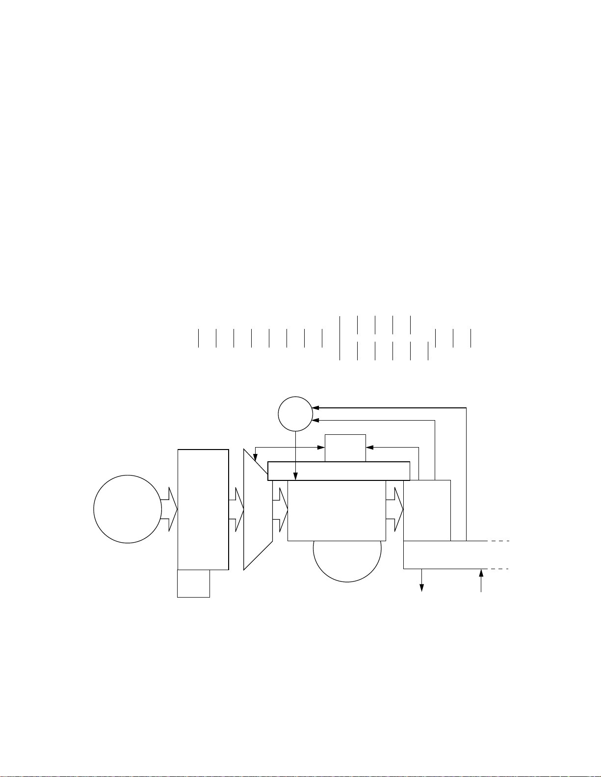
Figure 1.1 Overview of The 74K™ Pipeline
74K pipeline stages
I-cache
x4
IT
IFU
speculative
fetch
BHT
ID IS
x4
IB
IDU
issue
DD
DR DS
DM
reg
file
completion buffers
ALU
AGEN
x2
out-of-order execution
AF
EM EA
rename
map
D-cache
AC
EC
AB
ES
EB
AM
cache miss data
updates
GRU
x2
in-order
completion
memory pipeline
loads. stores, etc
external
read/write
WB
GC
read data
1.4.1 Notes on pipeline overview diagram (Figure 1.1):
Although this diagram is considerably simpler (and further abstracted from reality) than those in [SUM], there is still
a lot to digest. Rectangles and circles with a thick outline are major functional units — the rectangles are the active
Programming the MIPS32® 74K™ Core Family, Revision 02.14 14
Page 15

Introduction
units and each has a phrase (in italics) summarizing what it does. The three-letter acronyms match those found in the
detailed descriptions, and the pipeline stage names used in the detailed descriptions are across the top. Tosimplify the
picture the integer multiply unit and the (optional) floating point unit have been omitted — once you figure out what’s
going on, they shouldn’t be too hard to put back. So:
• The 74K core’s instruction fetch unit (“IFU”) is semi-autonomous. It’s 128 bits wide, and handles four instruc-
• Issue: the IDU (“instruction decode/dispatch unit”) keeps its own queue of instructions and tries to find two of
tions at a bite.
The IFU works a bit like a dog being taken for a walk. It rushes on ahead as long as the lead will stretch (the IFU,
processing instructions four at a time, can rapidly get ahead). Even though you’re in charge, your dog likes to go
first - and so it is with the IFU. Like a dog, the IFU guesses where you want to go, strongly influenced by the way
you usually go. If you make an unexpected turn there is a brief hiatus while the dog comes back and gets up front
again.
The IFU has a queue to keep instructions in when it’s running ahead of the rest of the CPU. This kind of design is
called a “decoupled” IFU.
them which can be issued in parallel. The instruction set is strictly divided into AGEN instructions (loads, stores,
prefetch, cacheops; conditional moves, branches and jumps) and ALU (everything else). If all else is good, the
IDU can issue one instruction of each type in every cycle. Instructions are marked with their place in the program
sequence, but are not necessarily issued in order. An instruction may leapfrog ahead of program order in the
IDU’s queue, if all the data it needs is ready (or at least will be ready by the time it’s needed).
Instructions which execute ahead of time can’t write data to real registers — that would disrupt the operation of
their program predecessors, which might execute later. It may turn out that such an instruction shouldn’t haverun
at all if there was a mispredicted branch, or an earlier-in-program-order instruction took an exception. Instead,
each instruction is assigned a completion buffer (CB) entry to receive its result. The CB entry also keeps informa-
tion about the instruction and where it came from. An instruction which is dependent on this one for a source reg-
ister value but runs soon afterward can get its data from the CB. CB-resident values can be found through the
rename map; that map is indexed by register number and points to the CB reserved by the instruction which will
write or has written a register value.
• out-of-orderexecution:theeffectoftheaboveisthatinstructions are issued in “dataflow” order,asdeterminedby
their dependencies on register values produced by other instructions. Up to 32 instructions can be somewhere
between available for issue and completed in the 74K core — those instructions are often said to be in flight. The
32 possible instructions correspond to 32 CB entries — 14 for AGEN instructions, 18 for ALU instructions.
Inside the “execution” box the AGEN and ALU instructions proceed strictly through two internally-pipelined
units of the same names. The two pipelines are in lockstep, and are kept that way. This sounds rigid, but is help-
ful. When the IDU issues an instruction, it does not have to know that an instruction’s data is ready “right now”:
it’s enough that the instruction producing that data is far enough along either execution pipeline. When no other
progress can be made its probably best to think of the IDU issuing a “no-op” or “bubble” into either or both pipe-
lines.
Most of the time the execution pipelines just keep running — the IDU tries to detect any reason why an instruc-
tion cannot run through either the AGEN or ALU pipe.When dependent instructions run close together, the data
doesn’t have time to go into a register or CB entry and be read out again. Instead it can flow down a dedicated
bypass connection between two particular pipestages — a routine trick used in pipelined logic. In the 74K core
there are bypasses interconnecting the AGEN and ALU pipelines, as well as within each pipeline. But whereas
pipeline multiplexing in a conventional design is controlled by comparing register numbers, in 74K cores we
compare completion buffer entry IDs.
15 Programming the MIPS32® 74K™ Core Family, Revision 02.14
Page 16

1.4 A brief guide to the 74K™ core implementation
There are a few simple instructions where the ALU produces its results in one clock (they’re listed in Table 4.3),
but most ALU instructions require two clocks: so, in the 74K core, dependent ALU instructions cannot usually
be run back-to-back. This would have a catastrophic effect on the performance of an in-order CPU, because
many instructions are dependent on their immediate predecessor. But an out-of-order CPU will run just fine,
because there are also a reasonable number of cases where an instruction is not dependent on its immediate pre-
decessor, so the pipeline can find something to run. The CPU will slow down if fed with a sequence of relatively
long-latency instructions each of which is dependent on its predecessor, of course. For example, in the AGEN
pipeline it takes four cycles to turn a load address into load data (assuming a cache hit). So chasing a chain of
pointers through memory will take at least four cycles per pointer.
• Optimistic issue: any instruction which is issued may yet not run to completion (there might be an exception on
an earlier-in-program instruction, for example). But some instructions are issued even though they are directly
dependent on something we’renot sure about — they’reissued optimistically. The most common example is that
instructions dependent on load data are issued as if we were confident the load will hit in the L1 cache.
Sometimes it turns out we were wrong. Notably, sometimes the load we’re dependent on suffers a cache miss. In
this case the hardware does the simplest thing: rather than attempt to single out the now unviable instruction, we
take a redirect on the load-value-consuming instruction we issued optimistically — that is, we discard all work
on that instruction and its successors, and ask the front end of the pipeline to start again from scratch, re-fetching
the instruction from the I-cache.
• In-order completion: at the end of the execution unit we take the oldest in-flight instruction (with luck, the sec-
ond-oldest too) and, if it’s results are ready, we graduate3one or two instructions (“GRU” stands for “graduation
unit”). Before we do that, we make a last minute check for exceptions: if one of the proposed graduates has
encountered a condition which should cause an exception it will be carrying that information with it, we discard
that instruction and do a redirect to the start of the appropriate exception handler. On successful graduation the
instruction’s results are copied from its CB entry back to a real CPU register, and it’s finished.
Because instruction effects aren’t “publicly” visible until graduation, our out-of-order CPU appears to the pro-
grammer to be running sequentially just like any other MIPS32-compliant CPU.
More details about out-of-order execution
That’s the basic flow. But the dual-issue, out-of-order design has some subtle points which can affect how programs
run:
• Mispredicted branches and redirects: because of the long pipeline, the 74K core relies very heavily on good
branch prediction. When the IFU guesses wrong about a conditional branch, or can’t compute the target for a
jump-register instruction, that’s detected somewhere down the AGEN pipeline (usually the “EC” stage). By then
we’ll have done a minimum of 12 cycles of work on the wrong path.
Whenever a branch is resolved the prediction result is sent back to the IFU to maintain its history table. For most
branches, the prediction result is sent back at the same time as we resolve the branch, which means that a few
branches which don’t graduate can affect the branch history. That’s OK, it was only a heuristic.
• Exceptions: can’t be resolved until we’re committed to running an instruction and have completed all its prede-
cessors. So they’re resolved only at graduation. That posts an exception handler address down to the front of a
pipe, clearing out all prefetched and speculatively-executed instructions in the process. There will be at least 19
3. Curiously,the alternative word to “graduation” (for an instruction being committed in an out-of-order design) is“retirement”:
a rather different stage of one’s career. I guess that from a software point of view we’reglad that the instruction is now grown
up and real, while the hardware is now ready to wave goodbye to it.
Programming the MIPS32® 74K™ Core Family, Revision 02.14 16
Page 17

Introduction
• Loads and Stores: the L1 cache lookup happens inside the out-of-order execution pipeline. But only loads which
cycles between the point where the exception is processed in the graduation unit and the time when the first
instruction of the exception handler graduates.
hit in the L1 cache are complete when they graduate. Other loads and stores graduate and then start actions in the
memory pipeline. It’s probably fairly obvious how a store can be “stored” — so long as the hardware keeps a note
of the address and data of the store, the cache/memory update can be done later. On the 74K core, even a write
into the L1 cache is deferred until after graduation. While the write is pending, the cache hardware has to keep a
note in case some later instruction wants to load the same value before we’ve completed the write; but that’s
familiar technology.
It’s less obvious that we can allow load instructions which L1-miss to graduate. But on the 74K core, loads are
non-blocking — a load executes, and results in data being loaded into a GP register at some time in the future.
Any later instruction which reads the register value must wait until the load data has arrived. So load instructions
are allowed to graduate regardless of how far away their data is. Once the instruction graduates its CB entry must
be given back, so data arriving for a graduated load is sent directly to the register file.
There’s another key reason why we did this: with only L1 accesses done out-of-order, loads and stores only
become visible outside the CPU after they graduate, so there’s no worry about other parts of the system seeing
unexpected effects from speculative instructions.
An instruction which depends on a load which misses will (unless it was a long, long way behind in instruction
sequence) have to wait. Most often the consuming instruction will become a candidate for issue before we know
whether the load hit in the L1 cache. In this case the dependent instruction is issued: we’re optimists, hoping for
a hit. If a consuming instruction reaches graduation and finds the load missed, we must do a “redirect”, re-fetching the consuming instruction and everything later in program order). Next time the consuming instruction is an
issue candidate, we’ll know the load has missed, and the consumer will not get issued until the load data has
arrived. The redirect for the consuming instruction is quite expensive (19 or more cycles), but in most cases that
overhead will be hidden in the time taken to return data for the cache miss.
Stores are less complicated. But since even the cache must not be updated until the store instruction graduates,
the memory pipeline is used for writing the L1 cache too: even store L1-hits result in action in the memory pipeline.
1.4.2 Branches and branch delays
The MIPS architecture defines that the instruction following a branch (the “branch delay slot” instruction) is always
executed4. That means that the CPU has one instruction it knows will be executed while it’s figuring out where a
branch is going. But with the 74K core’s long pipeline we don’t finally know whether a conditional branch should be
taken, and won’t have computed the target address for a jump-register,until about 8 stages down the pipeline. It’s better to guess (and pay the price when we’re wrong) than to wait to be certain. Several different tricks are used:
• The decoupled IFU (the electronic dog) runs ahead of the rest of the CPU by fetching four instructions per clock.
• Branch instructions are identified very early (in fact, they’re marked when instructions are fetched into the I–
cache). MIPS branch and jump instructions (at least those not dependent on register values) are easy to decode,
and the IFU decodes them locally to calculate the target address.
4. That’s not quite accurate: there are special forms of conditional branches called “branch likely” which are defined to execute
the branch delay slot instruction only when the branch is taken. Note that the “likely” part of the name has nothing to do with
branch prediction; the 74K core’s branch prediction system treats the “likelies” just like any other branches. The dependency
between a branch condition and the branch delay slot instruction is annoying to keep track of in an out-of-order machine, and
MIPS would prefer you not to use branch-likely instructions.
17 Programming the MIPS32® 74K™ Core Family, Revision 02.14
Page 18

1.4 A brief guide to the 74K™ core implementation
The IFU’s branch predictor guesses whether conditional branches will be taken or not - it’s not magic, it uses a
BHT (a “Branch History Table”) of what happened to branches in the past, indexed by the low bits of the loca-
tion of the branch instruction. This particular hardware is an example of Combined branch prediction (majority
voting between three different algorithms, one of which is gshare; if you want to know, there’s a good wikipedia
article whose topic name is “Branch Predictor”). The branch predictor is taking a good guess. It can seem surprising that the predictor makes no attempt to discover whether the history stored in a BHT slot is really that of
the current branch, or another one which happened to share the same low address bits; we’re going to be wrong
sometimes. It guesses correctly most of the time.
In this way the IFU can predict the next-instruction address and continue to run ahead.
• When the IFU guesses wrong, it doesn’t know (the dog just rushes ahead until its owner reaches the fork). The
branch mispredict will be noticed once the branch instruction has been issued and carried through to the AGEN
“EC” stage, and is executed in its full context (“resolved”). On detecting a mispredict, the CPU must discard the
instructions based on the bad guess (which will not have graduated yet, so will not have changed any vital
machine state) and start fetching instructions from the correct target5. The exact penalty paid by a program which
suffers a mispredict depends on how busy the execution unit is, and how early it resolves the branch; the minimum penalty is 12 cycles.
• Even when we guess right, the branch target calculation in the IFU takes a little while to operate. A rapid
sequence of correctly-predicted branches can empty the queues, causing a program to run slower.
• Jump-register instruction targets are unpredictable: the IFU has no knowledge of register data and can’t in gen-
eral anticipate it. But jump-register instructions are relatively rare, except for subroutine returns. In the MIPS
ISA you return from subroutines using a jump-register instruction, jr $31 (register 31 is, by a strong convention, used to hold the return address). So on every call instruction, the IFU pushes the return address onto a small
stack; and on every jr $31 it pops the value of the stack and uses that as its guess for the branch target6.
We have no way of knowing the target of a jr instruction which uses a register other than $31. When we find
one of those, instruction fetch stops until the correct address is computed up in the AGEN pipeline, 12 or more
clocks later.
1.4.3 Loads and load-to-use delays
Even short-pipeline MIPS CPUs can’t deliver load data to the immediately following instruction without a delay,
even on a cache hit. Simple MIPS pipelines typically deliver the data one clock later: a one clock “load-to-use delay”.
Compilers and programmers try to put some useful and non-dependent operation between the load and its first use.
The 74K core’s long pipeline means that a full D-cache hit takes four clocks to return the data, not two: that would be
a three-clock “load-to-use delay”. A pair of loads dependent on each other (one fetches the other’s base address) must
be issued at least four cycles apart (that’s optimistic, hoping-for-a-hit timing).
But the AGEN and ALU pipelines are “skewed”, with ALU results delivered a cycle later than AGEN results. That
means that when an ALU operation is dependent on a load, it can be issued only three cycles after the load. There’s a
price to pay: a load/store whose base address is computed by a preceding ALU instruction must be issued a clock
5. In “branch-likely” variants of conditional branch instructions a mispredict means we also did the wrong thing with the
instruction in the branch delay slot. To fix that up, we need to refetch the branch itself, so the penalty is at least one cycle
higher.
6. The return-stack guess will be wrong for subroutines containing nested calls deeper than the size of the return stack; but subroutines high up the call tree are much more rarely executed, so this isn’t so bad.
Programming the MIPS32® 74K™ Core Family, Revision 02.14 18
Page 19

Introduction
later than an ALU instruction with the same dependency — that’s usually a three cycle delay, because most ALU
operations already take an extra clock to produce their result.
It’s like the skewed pipeline which experts in MIPS Technologies’ 24K® family might remember, and has the same
motivation: ALU operations dependent on recent loads are more common than loads dependent on recent ALU operations.
1.4.4 Queues, Resource limits and Consequences
Queues which can fill up include:
• Cache refills in flight: Is dependent on the size of the “FSB” queue - this and other queues are described in more
detail under Section 3.3, "Reads, writes and synchronization". The CPU does not wait for a cache refill process
— at least not until it needs data from the cache miss. But in practice most load data is used almost at once, so the
CPU will stop very soon after a miss. As a result, you’re unlikely to ever have four refills in flight unless you are
using prefetch or otherwise deliberately optimizing loops. If a series of aggressive prefetches miss often enough,
the fourth outstanding load-miss will use the last FSB entry, preventing further loads from graduating and eventually blocking up the whole CPU until the load data returns. It’s likely to be good practice for code making conscious use of prefetches to ration itself to a number of operations slightly less than the size of the FSB.
• Non-blocking loads to registers (nine): there are nine entries in the “LDQ”, each of which remembers one out-
standing load, and which register the data is destined to return to. Compiled code is unlikely to reach this limit. If
you write carefully optimized code where you try to fill load-use delays (perhaps for data you think will not hit in
the D-cache) you may hit this problem.
• Lines evicted from the cache awaiting writeback (4+): writes are collected in the “WBB” queue. The 74K core’s
ability to write data will in almost all circumstances exceed the bandwidth available to memory; so a long enough
burst of uncached or write-through writes will eventually slow to memory speed. Otherwise, you’re unlikely to
suffer from this.
• Queues in the coprocessor interface: the 74K core hides its out-of-order character from any coprocessors, so
coprocessor hardware need be no more complicated than it is for MIPS Technologies’24Kcore. The coprocessor
hardware sees its instructions strictly in order. Each coprocessor instruction also makes its own way through the
integer execution unit. Between the execution unit and coprocessor there are some queues which can fill up:
• IOIQ (8 entries): instructions being issued — strictly in program order — to a coprocessor.
• CBIDQ (8 entries): data being returned from a coprocessor by an instruction which writes a GP register. But
prior to graduation the data goes back to a completion buffer (hence the queue acronym).
• CLDQ (8 entries): track data being loaded to coprocessor registers (the job done for the GPRs by the LDQ
above). CLDQ data isn’t necessarily provided in instruction sequence: in particular MIPS Technologies
floating-point unit accepts FP load data as and when it arrives, making FP loads non-blocking.
The dispatch process stalls (flooding the ALU and AGEN pipes with bubbles) when there is no space in any of
these queues.
19 Programming the MIPS32® 74K™ Core Family, Revision 02.14
Page 20

1.4 A brief guide to the 74K™ core implementation
Programming the MIPS32® 74K™ Core Family, Revision 02.14 20
Page 21

Chapter 2
Initialization and identity
What happens when the CPU is first powered up? These functions are perhaps more often associated with a ROM
monitor than an OS.
2.1 Probing your CPU - Config CP0 registers
The four registers Config and Config1-3 are 32-bit CP0 registers which contain information about the CPU’s capabilities. Config1-3 are strictly read-only. The few writable fields in Config — notably Config[K0] — are there for
historic compatibility, and are typically written once soon after bootstrap and never changed again.
The 74K core also defines Config7 for some implementation-specific settings (which most programmers will never
use).
Broadly speaking the registers have these roles:
Table 2.1 Roles of Config registers
Config A mix of historical and CPU-dependent information, described in Figure 2.1 below. Some
fields are writable.
Config1 Read-only, strictly totheMIPS32architecture. Config1 shows the primary cache configuration
Config2
Config3 Read-only, strictly to Release 2 of the [MIPS32] architecture.
Config6 Provides information about the presence of optional extensions to the base MIPS32 architec-
Config7 74K-core-specific, with both read-only and writable fields. It’s a strong convention that the
and basic CPU capabilities, while Config2showsinformationaboutL2 and L3 caches, if fitted
(the L2 and the L3 cache is unavailable in 74K family cores). Shown in Figure 2.2 and Figure
2.3 below.
More CPU capability information.
ture in addition to those specified in Config2 and Config3.
writable fields should default to “expected” behavior, so beginners may simply leave these
fields alone. The fields are described later, in Section B.2.1 “The Config7 register”.
While initializing your CPU, you might also want to look at the EBase register, which can be used to relocate your
exception entry points: see Figure 5.2 and the text round it.
Programming the MIPS32® 74K™ Core Family, Revision 02.14 21
Page 22

2.1 Probing your CPU - Config CP0 registers
2.1.1 The Config register
Figure 2.1 Fields in the Config Register
31 30 28 27 25 24 23 22 21 20 19 18 17 16 15 14 13 12 10 9 7 6 4 3 2 0
M K23 KU ISP DSP UDI SB 0 WC MM 0 BM BE AT AR MT 0 VI K0
12 2 01 0 1 02
In Figure 2.1:
M: reads 1 if Config1 is available (it always is).
K23, KU, K0: set the cacheability attributes of chunks of the memory map by writing these fields. All share a 3-bit
encoding with the cacheability field found in TLB entries, which is described in Table 3.3 in Section
3.4.2 “Cacheability options”.
Config[K0] sets the cacheability of kseg0, but it would be very unusual to make that anything other than cacheable
(on different, cache-coherent CPUs, it may want to be set to cacheable-coherent). The power-on value of this standard
field is not mandated by the [MIPS32] architecture; but the 74K core follows the recommendation to set it to "2",
making "kseg0" uncached. That can be surprising; early system initialization software typically re-writes it to "3" in
order that kseg0 will be cached, as expected.
If your
74K core-based system uses fixed mapping instead of having a TLB, Config[K23] is for program addresses
0xC000.0000-0xFFFF.FFFF (the “kseg2” and “kseg3” areas), while Config[KU] is for program addresses
0x0000.0000-0x7FFF.FFFF (the “kuseg” area). If you have a TLB, these regions are mapped and these fields are
unused (write only zeroes to them).
ISP, DSP: read 1 if I-side and/or D-side scratchpad (SPRAM) is fitted, see Section 3.6, "Scratchpad memory/
SPRAM".
(Don’t confuse this with the MIPS DSP ASE, whose presence is indicated by Config3[DDSP].)
UDI: reads 1 if your core implements user-defined "CorExtend" instructions. “CorExtend” is available on cores whose
name ends in "Pro".
SB: read-only "SimpleBE" bus mode indicator. If set, means that this core will only do simple partial-word transfers on
its OCP interface; that is, the only partial-word transfers will be byte, aligned half-word and aligned word.
If zero, it may generate partial-word transfers with an arbitrary set of bytes enabled (which some memory controllers
may not like).
WC: Warning: this is a diagnostic/test field, not intended for customer use, and may vanish without notice from a
future version of the core.
Set this 1 to make the Config1[IS] and Config1[DS] fields writable, which allows you to reduce the number of avail-
able L1 I- and D-cache ``sets per way'', and shrink the usable cache size. You'd never want to do this in a real system,
but it is conceivable it might be useful for debug or performance analysis. If you have an L2 cache configured, then
this makes Config2[SS] writable in the same way.
MM: writable: set 1 if you want writes resulting from separate store instructions in write-through mode merged into a
single (possibly burst) transaction at the interface. This has no affect on cache writebacks (which are always whole
blocks together) or uncached writes (which are never merged).
Programming the MIPS32® 74K™ Core Family, Revision 02.14 22
Page 23

Initialization and identity
BM: read-only - tells you whether your bus uses sequential or sub-block burst order; set by hardware to match your sys-
tem controller.
BE: reads 1 for big-endian, 0 for little-endian.
AT: MIPS32 or MIPS64 compliance On 74K family cores it will read “0”, but the possible values are:
0 MIPS32
1 MIPS64 instruction set but MIPS32 address map
2 MIPS64 instruction set with full address map
AR: Architecture revision level. On 74K family cores it will read “1”, denoting release 2 of the MIPS32 specification.
0 MIPS32/MIPS64 Release 1
1 MIPS32/MIPS64 Release 2
MT: MMU type (all MIPS Technologies cores may be configured as type 1 or 3):
0 None
1 MIPS32/64 compliant TLB
2 “BAT” type
3 MIPS-standard fixed mapping
VI: 1 if the L1 I-cache is virtual (both indexed and tagged using virtual address). No contemporary MIPS Technologies
core has a virtual I-cache.
K0: as described in the notes above on Config[K23] etc, this field determines the cacheing behaviour of the fixed kseg0
memory region .
2.1.2 The Config1-2 registers
These two read-only registers tell you the size of the TLB, and the size and organization of L1, L2 and L3 caches (a
zero “line size” is used to indicate a cache which isn’t there). They’re best described together.
Config1 has some fields which tell you about the presence of some of the older extensions to the base MIPS32 archi-
tecture are implemented on this core. These bits ran out, and other extensions are noted in Config3.
Figure 2.2 Fields in the Config1 Register
31 30 25 24 22 21 19 18 16 15 13 12 10 9 7 6 5 4 3 2 1 0
M MMUSize IS IL IA DS DL DA C2 MD PC WR CA EP FP
1434301111
Figure 2.3 Fields in the Config2 Register
31 30 28 27 24 23 20 19 16 15 13 12 11 8 7 4 3 0
M TU TS TL TA SU L2B SS SL SA
10 0 0 0 0 0
Config1[M]: continuation bit, 1 if Config2 is implemented.
23 Programming the MIPS32® 74K™ Core Family, Revision 02.14
Page 24

2.1 Probing your CPU - Config CP0 registers
Config1[MMUSize]: the size of the TLB array (the array has MMUSize+1 entries).
Config1[IS,IL,IA,DS,DL,DA]: for each cache this reports
S
Number of sets per way. Calculate as: 64 × 2
L
Line size. Zero means no cache at all, otherwise calculate as: 2 × 2
A Associativity/number of ways - calculate as A + 1
S
L
So if (IS, IL, IA) is (2,4,3) you have 256 sets/way, 32 bytes per line and 4-way set associative: that’s a 32Kbyte cache.
Config1[C2,FP]: 1 if coprocessor 2 or or an FPU (coprocessor 1) fitted, respectively. A coprocessor 2 would be a cus-
tomer-designed coprocessor.
Config1[MD]: 1 if MDMX ASE is implemented in the floating point unit (very unlikely for the 74K core).
Config1[PC]: there is at least one performance counter implemented, see Section 8.4, "Performance counters".
Config1[WR]: reads 1 because the 74K core always has watchpoint registers, see Section 8.3, "CP0 Watchpoints".
Config1[CA]: reads 1 because the MIPS16e compressed-code instruction set is available (as it generally is on MIPS
Technologies cores).
Config1[EP]: reads 1 because an EJTAG debug unit is always provided, see Section 8.1, "EJTAG on-chip debug unit".
Config2[M]: continuation bit, 1 if Config3 is implemented.
Config2[TU]: implementation-specific bits related to tertiary cache, if fitted. Can be writable.
Config2[TS,TL,TA]: tertiary cache size and shape - encoded just like Config1[IS,IL,IA] which see above.
Config2[SU]: implementation-specific bits for secondary cache, if fitted. Can be writable.
Config2[L2B]: Set to disable L2 cache (“bypass mode”). Setting this bit also forces Config2[SL] to 0 — most OS code
will conclude that there isn't an L2 cache on the system, which can be useful.
Writing this bit controls a signal out to the L2 cache hardware. However, reading it does not read back what you just
wrote: it reflects the value of a signal sent back from the L2 cache. With MIPS Technologies' L2 cache logic, that
feedback signal will reflect the value you just wrote, with some implementation-dependent delay (it's unlikely to be
100 cycles, but it could easily be more than 10). For more details refer to “MIPS® PDtrace™ Interface and Trace
Control Block Specification”, MIPS Technologies document MD00439. Current revision is 4.30: you need revision 4
or greater to get multithreading trace information. [L2CACHE].
Config2[SS,SL,SA]: secondary cache size and shape, encoded like Config1[IS,IL,IA] above.
2.1.3 The Config3 register
Config3 provides information about the presence of optional extensions to the base MIPS32 architecture. A few of
them were in Config2, but that ran out of bits.
Figure 2.4 Config3 Register Format
31 30 29 28 14 13 12 11 10 9 8 7 6 5 4 3 2 1 0
M 0 CMGCR ULRI 0 DSP2P DSPP
CTXTC
0 VEIC VInt SP
CDMM
MT SM TL
Programming the MIPS32® 74K™ Core Family, Revision 02.14 24
Page 25

Initialization and identity
31 30 29 28 14 13 12 11 10 9 8 7 6 5 4 3 2 1 0
011100
Fields shown in Figure 2.4 include:
Config3[M]: continuation bit which is zero, because there is no Config4.
Config3[CMCGR]: reads 1 if Global Control Register in the Coherence Manager are implemented and the
CMGCRBase register is present. Reads 0 otherwise
Config3[ULRI]: reads 1 if the core implements the UserLocal register, typically used by software threads packages.
DSP2P, DSPP: DSPP reads 1 if the MIPS DSP extension is implemented — as described in Chapter 7, “The
MIPS32® DSP ASE” on page 87. If so, DSP2P reads 1 if your CPU conforms to revision 2 of the DSP ASE — as
the 74K core does.
CTXTC: reads 1 when the ContextConfig register is implemented. The width of the BadVPN2 field in the Context
register depends on the contents of this register.
VEIC: read-only bit from the core input signal SI_EICPresent which should be set in the SoC to alert software to the
availability of an EIC-compatible interrupt controller, see Section 5.2, "MIPS32® Architecture Release 2 - enhanced
interrupt system(s)".
VInt: reads 1 when the 74K core can handle vectored interrupts.
SP: reads 0 when the 74K core does not support sub-4Kbyte page sizes.
CDMM: reads 0 when the 74K core does not support the Common Device Memory Map.
SM: reads 0, the 74K core does not handle instructions from the "SmartMIPS" ASE.
TL: reads 1 if your core is configured to do instruction trace.
2.1.4 The Config6 register
Config3 provides information about the presence of optional extensions to the base MIPS32 architecture in addition to
those specified in Config2 and Config3.
Figure 2.5 Config6 Register Format
31 15 14 13 12 10 9 8 7 2 1 0
0 SPCD SYND
SPCD disables performance counter clock shutdown. The primary use of this bit is to keep performance counters
alive when the core is in sleep mode.
SYND disables Synonym tag update. By default, all synonym load misses will opportunistically update the tag so
that subsequent loads will hit at lookup.
IFUPerfCtl NMRUP
NMRUD 0
JRCP JRCD
IFUPerfCtl encodes IFU events that provide debug and performance information for the IFU pipeline.
NMRUP indicates that a Not Most Recently Used JTLB replacement scheme is present.
25 Programming the MIPS32® 74K™ Core Family, Revision 02.14
Page 26
2.2 PRId register — identifying your CPU type
NMRUD disables the Most Recently Used JTLB replacement scheme bit.
JRCP indicates that a JR Cache is implemented.
JRCD indicates that JR Cache Prediction is enabled.
2.1.5 CPU-specific configuration — Config7
Config7 is packed with implementation-specific fields. Most of the time, you leave them alone (a few of them might
sometimes need to be set as required by your SoC designer). So we’ve left these registers defined in the all-CP0
appendix, in Section B.2.1 “The Config7 register”.
2.2 PRId register — identifying your CPU type
This register identifies the CPU to software. It’s appropriately printed as part of the start-up display by any software
telling the world about the CPU on start-up; but when portable software is configuring itself around different CPU
attributes, it’s always preferable to sense those attributes directly — look in other Config registers, or perhaps use a
directed software probe.
Figure 2.6 Fields in the PRId Register
31 24 23 16 15 8 7 5 4 2 1 0
CoOpt CoID Imp
Major Minor Patch
1 0x97
Rev
PRId[CoOpt]: Whatever is specified by the SoC builder who synthesizes the core — refer to your SoC manual. It
should be a number between 0 and 127 — higher values are reserved by MIPS Technologies.
PRId[CoID]: Company ID, which in this case is “1” for MIPS Technologies Inc.:
PRId[Imp]: Identifies the particular processor, which in this case is 0x97 for the 74K family. Any processor with differ-
ent CP0 features must have a new PRId field.
PRId[Rev]: The revision number of the core design, used to index entries in errata lists etc. By MIPS Technologies’
convention the revision field is divided into three subfields: a major and minor number; with a nonzero "patch" revi-
sion number is for a release with no functional change. Core licensees can consult [ERRATA] for authoritative infor-
mation about the revision IDs associated with releases of the 74K core.
The following incomplete and not up-to-date table of historical revisions is provided as a guide to program-
mers who don’t have [ERRATA] on hand:
Table 2.2 74K™® core releases and PRId[Revision] fields
Release
Identifier
2_0_* 1.0.0 / 0x20 First (GA) release of the 34K core September 30, 2005
2_1_* 2.1.0 / 0x44 MR1 release. Bug fixes, 8KB cache support. March 10, 2006
Programming the MIPS32® 74K™ Core Family, Revision 02.14 26
PRId[Revision]
Maj.min.patch/hex Description Date
Page 27

Initialization and identity
2_2_0 2.2.0 / 0x48 Allow up to 9 TCs, alias-free 64KB L1 D-cache option. August 31, 2006
2_2_1 2.2.1 / 0x49 Enable use of MIPS SOC-it® L2 Cache Controller. October 12, 2006
2_3_* 2.3.0 / 0x4c Less interlocks round cache instructions, relocatable
2_4_* 2.4.0 / 0x50 New UserLocal register,alias-proofI-cache hit-invalidate
2_5_* 2.5.0/0x54 Errata fixes January, 2009
1_1_* 1.1.0/0x24 Errata fixes January, 2009
1_2_* 1.2.0/0x28 Feature updates: improved low power support, fast debug
2_0_* 2.0.0 / 0x40 General availability of 24K core. March 19, 2004
3_0_* 3.0.0 / 0x60 COP2 option improvements. September 30, 2004
3_2_* 3.2.0 / 0x68 PDtrace available. March 18, 2005
3_4_* 3.4.0 / 0x6c ISPRAM (I-side scratchpad) option added June 30, 2005
3_5_* 3.5.0 / 0x74 8KB cache option December 30, 2005
3_6_* 3.6.0 / 0x78 L2 support., 64KB alias-free D-cache option, option to
3_7_* 3.7.0 / 0x7c Less interlocks round cache instructions, relocatable
4_0_* 4.0.0 / 0x80 New UserLocal register,alias-proofI-cache hit-invalidate
4_1_* 4.1.0/0x84 Errata fixes January, 2009
2_0_* 2.0.0 / 0x40 General availability of 24KE core. June 30, 2005
2_1_* 2.1.0 / 0x44 8KB cache option December 30, 2005
2_2_* 2.2.0 / 0x48 L2 support., 64KB alias-free D-cache option, option to
2_3_* 2.3.0 / 0x4c Less interlocks round cache instructions, relocatable
2_4_* 2.4.0 / 0x50 New UserLocal register,alias-proofI-cache hit-invalidate
2_5_0 2.5.0/0x54 Errata fixes January, 2009
1_0_* 1.0.0 / 0x20 Early-access release of 74K family RTL. January 31, 2007
2_0_0* 2.0.0 / 0x40 First generally-available release of 74K family core. May 11, 2007
2_1_0* 2.1.0 / 0x44 Can wait with interrupts disabled. October 31, 2007
Table 2.2 74K™® core releases and PRId[Revision] fields
January 3, 2007
reset exception vector location.
October 31, 2007
operation, can wait with interrupts disabled, per-TC performance counters.
July, 2009
channel, on-chip PDtrace buffers
July 12, 2006
haveupto 8 outstanding cache misses(previousmaximum
4).
January 3, 2007
reset exception vector location.
October 31, 2007
operation, can wait with interrupts disabled.
July 12, 2006
haveupto 8 outstanding cache misses(previousmaximum
4).
January 3, 2007
reset exception vector location.
October 31, 2007
operation, can wait with interrupts disabled.
27 Programming the MIPS32® 74K™ Core Family, Revision 02.14
Page 28

2.2 PRId register — identifying your CPU type
Programming the MIPS32® 74K™ Core Family, Revision 02.14 28
Page 29

Chapter 3
Memory map, caching, reads, writes and translation
In this chapter:
• Section 3.1, "The memory map": basic memory map of the system.
• Section 3.3, "Reads, writes and synchronization"
• Section 3.4, "Caches"
• Section 3.6, "Scratchpad memory/SPRAM": optional on-chip, high-speed memory (particularly useful when
dual-ported to the OCP interface).
• Section 3.8, "The TLB and translation": how translation is done and supporting CP0 registers.
3.1 The memory map
A 74K core system can be configured with either a TLB (virtual memory translation unit) or a fixed memory mapping.
A TLB-equipped sees the memory map described by the [MIPS32] architecture (which will be familiar to anyone
who has used a 32-bit MIPS architecture CPU) and is summarized in Table 3.1. The TLB gives you access to a full
32-bit physical address on the system interface. More information about the TLB in Section 3.8, "The TLB and
translation".
Table 3.1 Basic MIPS32® architecture memory map
Segment Virtual range What happens to accesses here?
Name
kuseg 0x0000.0000-0x7FFF.FFFF The only region accessible to user-privilege programs.
Mapped by TLB entries.
kseg0 0x8000.0000-0x9FFF.FFFF a fixed-mapping window onto physical addresses
0x0000.0000-0x1FFF.FFFF. Almost invariably cacheable - but in fact other choices are available, and are
selected by Config[K0], see Figure 2.1.
Accessible only to kernel-privilege programs.
kseg1 0xA000.0000-0xBFFF.FFFF a fixed-mapping window onto the same physical
address range 0x0000.0000-0x1FFF.FFFF as “kseg0”
- but accesses here are uncached.
Accessible only to kernel-privilege programs.
kseg2 0xC000.0000-0xDFFF.FFFF Mapped through TLB, accessible with supervisor or
sseg
kseg3 0xE000.0000-0xFFFF.FFFF Mapped through TLB, accessible only with kernel
kernel privilege (hence the alternate name).
privileges.
Programming the MIPS32® 74K™ Core Family, Revision 02.14 29
Page 30
3.2 Fixed mapping option
With the fixed mapping option, virtual address ranges are hard-wired to particular physical address windows, and
cacheability options are set through CP0 register fields as summarized in Table 3.2:
Table 3.2 Fixed memory mapping
Segment Virtual range Physical range Cacheability
Name bits from
kuseg 0x0000.0000-0x7FFF.FFFF 0x4000.0000-0xBFFF.FFFF Config[KU]
kseg0 0x8000.0000-0x9FFF.FFFF 0x0000.0000-0x1FFF.FFFF Config[K0]
kseg1 0xA000.0000-0xBFFF.FFFF 0x0000.0000-0x1FFF.FFFF (uncached)
kseg2/3 0xC000.0000-0xFFFF.FFFF 0xC000.0000-0xFFFF.FFFF Config[K23]
Even in fixed-mapping mode, the cache parity error status bit Status[ERL] still has the effect (required by the MIPS32
architecture) of taking over the normal mapping of “kuseg”; addresses in that range are used unmapped as physical
addresses, and all accesses are uncached, until
Status[ERL] is cleared again.
3.3 Reads, writes and synchronization
3.2 Fixed mapping option
The MIPS architecture permits implementations a fair amount of freedom as to the order in which loads and stores
appear at the CPU interface. Most of the time anything goes: so long as the software behaves correctly, the MIPS
architecture places few constraints on the order of reads and writes seen by some other agent in a system.
3.3.1 Read/write ordering and cache/memory data queues in the 74K™ core
To understand the timing of loads and stores (and sometimes instruction fetches), we need to say a little more about
the internal construction of the 74K core. In order to maximize performance:
• Loads are non-blocking: execution continues “through” a load instruction, and only stops when the program tries
to use the GPR value it just loaded.
• Writes are “posted”: a write from the core is put aside (the hardware stores both address and data) until the CPU
can get access to the system interface and send it off. Even writes which hit in the cache are posted, occurring
after the instruction graduates.
• Cache refills are handled after the “missing” load has graduated: most of the time the CPU will quite soon get
hung up on an instruction which needs the data from the miss, but this is not necessarily the case. The CPU runs
on after the load instruction, with the memory pipeline logic remembering and handling the load completion.
All of these are implemented with “queues”, called the LDQ, WBB and FSB (for “fill/store buffer” — it’s used both
for writes which hit and for refills after a cache miss) respectively. All the queues handle data first-come, first served.
The WBB and FSB queues need to be snooped - a subsequent store to a location with a load pending had better not be
allowed to go ahead until the original load data has reached the cache, for example. So each queue entry is tagged
with the address of the data it contains.
An LDQ entry is required for every load that misses in the cache. This queue allows the CPU to keep running even
though there are outstanding loads. When the load data is finally returned from the system, the LDQ and the main
core logic act together to write this data into the correct GPR (which will then free up any instructions whose issue is
blocked waiting for this data).
Programming the MIPS32® 74K™ Core Family, Revision 02.14 30
Page 31

Memory map, caching, reads, writes and translation
The WBB (Write Back Buffer) queue holds data waiting to be sent out over the system interface, either from D-cache
writebacks or uncached/write-through store instructions.
FSB (Fill Store buffer) queue entries are used to hold data that is waiting to be written into the D-cache. An FSB entry
gets used during a cache miss (when it holds the refill data), or a write which hits in the cache (when it holds the data
the CPU wrote). Loads and stores snoop the FSB so that accesses to lines “in flight” can be dealt with correctly.
All this has a number of consequences which may be visible to software:
• Number of non-blocking loads which may be pending: the CPU has nine LDQ entries. That limits the number of
outstanding loads.
• Hit-under-miss: the D-cache continues to supply data on a hit, even when there are outstanding misses with data
in flight. FSB entries remember the in-flight data. So it is quite normal for a read which hits in the cache to be
“completed” - in the sense that the data reaches a register - before a previous read which missed.
• Write-under-miss: the CPU pipeline continues and can generate external store cycles even though a read is pending, so long as WBB slots are available. The 74K core’s “OCP” interface is non-blocking too (reads consist of
separate address and data phases, and writes are permitted between them), so this behavior can often be visible to
the system.
• Miss under miss: the 74K core can continue to run until the pending read operations exhaust FSB or LDQ entries.
More often, of course, it will try to use the data from the pending miss and stall before it gets that far.
• Core interface ordering: at the core interface, read operations may be split into an address phase and a later data
phase, with other bus operations in between.
The 74K core - as is permitted by [MIPS32] - makes only limited promises about the order in which reads and
writes happen at the system interface. In particular, uncached or write-through writes may be overtaken by cache
line reads triggered by a load/store cache miss later in sequence. However, uncached reads and writes are always
presented in their program sequence. When some particular program needs to do things “really in order”, the
sync instruction can help, as described in the next section.
Cache management operations interact with several queues: see Section 3.4.6 “L1 Cache instruction timing”.
3.3.2 The “sync” instruction in 74K™ family cores
If you want to be sure that some other agent in the system sees a pair of transactions to uncached memory in the order
of the instructions that caused them, you should put a sync instruction between the instructions. Other MIPS32/64-
compliant CPUs may reorder loads and stores even more; portable code should use sync7.
But sometimes it’s useful to know more precisely what sync does on a particular core. On 74K sync:
• Stalls graduation (preventing any later load/store from graduating and becoming externally visible) until all
pending reads, cached writes and OCP writes are completed — that is, until the FSB and WBB are empty;
• In some systems the CPU will also generate a synchronizing transaction on the OCP system interface if
Config7[ES] bit is set
8
. Not all systems do this. See Section B.2.1 “The Config7 register” for more details.
7. Note that sync is described as only working on “uncached pages or cacheable pages marked as coherent”. But sync also
acts as a synchronization barrier to the effects produced by routine cache-manipulation instructions - hit-writeback and hitinvalidate.
31 Programming the MIPS32® 74K™ Core Family, Revision 02.14
Page 32

3.4 Caches
A new set of lightweight SYNC instructions have been introduced. As compared to the completion barrier, the ordering barrier is a lighter-weight operation as it does not require the specified instructions before the SYNC to be already
completed. Instead it only requires that those specified instructions which are subsequent to the SYNC in the instruction stream are never re-ordered for processing ahead of the specified instructions which are before the SYNC in the
instruction stream. This potentially reduces how many cycles the barrier instruction must stall before it completes.
Because the core processes loads and stores in order, ordering barriers are much lighter weight. Details about the set
of supported lightweight SYNC instructions can be found in the Software User’s Reference Manual
3.3.3 Write gathering and “write buffer flushing” in 74K™ family cores
We mentioned above that writes to the system (whether uncached writes or cache write-backs) are performed somewhat lazily, the write being held in the WBB queue until a convenient moment. That can have two system-visible
effects:
• Writes can happen later than you think. Your write will happen before the next uncached read or write, but that’s
all you know. And your write might still be posted somewhere in a system controller, unless you know your system is built to prevent it. Sometimes it’s better to code a dummy uncached read from a nearby location (which
will “flush out” buffered writes on pretty much any system).
• If your cache is configured for write-through, then cached writes to locations in the same “cache line”-sized
chunk of memory may be gathered - stored together in the WBB, and then dealt with by a single “wider” OCP
write than the one you originally coded. Sometimes, this is what you want. When it isn’t, put a
your successive writes. Regular uncached writes are never merged, but special “uncached accelerated” writes
may be — see Section 3.4.3 below.
sync between
3.4 Caches
Most of the time caches just work and are invisible to software... though your programs would go twenty times slower
without them. But this section is about when caches aren’t invisible any more.
Like most modern MIPS CPUs, the 74K core has separate primary I- and D-caches. They are virtually-indexed and
physically-tagged, so you may need to deal with cache aliases, see Section 3.4.9, "Cache aliases". The design pro-
vides for 16Kbyte, 32Kbyte or 64Kbyte caches; but the largest of those are likely to come with some speed penalty.
The 74K core’s primary caches are 4-way set associative.
Your 74K core can optionally be built with a L2 (level 2 or secondary) cache. see section below for details.
But don’t hard-wire any of this information into your software. Instead, probe the Config1 register defined by
[MIPS32] (and described in ) to determine the shape and size of the L1 and any L2 cache.
3.4.1 The L2 cache option
The L2 cache is an option available to your SoC builder. Basic facts and figures:
• The L2 cache is attached to the core’s standard 64-bit OCP system interface, and when you fit it everything else
is attached to the core through the L2 cache, which has a system-side interface for that purpose. The core-side
8. This will be a read with the signal OC_MReqInfo[3] set. Handling of this transaction is system dependent, but a typical system controller will flush any external write buffers and complete all pending transactions before telling the CPU that the
transaction is completed. Ask your system integrator how it works in your SoC.
Programming the MIPS32® 74K™ Core Family, Revision 02.14 32
Page 33

Memory map, caching, reads, writes and translation
interface is enhanced and augmented to support cache instructions targeted at the L2, and to carry back performance counter information and so on.
• The L2 ‘s size can be 128Kbytes, 256Kbytes, 512Kbytes or 1Mbyte. However, there are options which allow the
SoC builder to have one or more of the ways of the cache memory array visible as normal system memory
instead. There’s very little in this manual about that option. — see “MIPS® PDtrace™ Interface and Trace
Control Block Specification”, MIPS Technologies document MD00439. Current revision is 4.30: you need
revision 4 or greater to get multithreading trace information. [L2CACHE].
• The L2 cache is indexed and tagged with the physical address, so is unaffected by cache aliases.
• Cache lines are either 32 bytes long (matching the L1 caches) or 64 bytes. The L2 cache’s memories are accessed
256 bits at a time internally, though it has 64-bit interfaces.
• It can be configured with 4-way or 8-way set-associative organization. In a 4-way cache the line replacement pol-
icy is “least recently used” (LRU); true LRU is impractical for an 8-way set associative cache, so something simpler (a “pseudo-LRU”) is used.
• The cache has an option for error detection and correction. 1-bit data errors can be corrected and all 2-bit errors
detected with an 8-bit-per-doubleword ECC field. Check bits are provided on cache tags, too. If your L2 has ECC
fitted, ErrCtl[L2P] will be writable — see Section 3.4.17 “ErrCtl register” for details.
• The cache is write-back but does not allocate a line on a write miss (write miss data is just sent directly to the sys-
tem memory). It is write-through for memory regions which request that policy -- see Section
3.4.2 “Cacheability options” for details.
• The L2 cache can run synchronously to the CPU core, but (particularly for memory arrays larger than
256Kbytes) would typically then be the critical path for timing. It will more often use a 1:2 or 2:3 clock ratio.
The L2’s far-side OCP interface may run at any of a wide range of ratios from the L2 clock down.
• In an effort to keep everything going the cache manages multiple outstanding transactions (it can handle as many
as 15 outstanding misses). Misses are resolved and responses sent as they happen, not in the order of presentation.
• Latency: the L2 logic allows the memory access to be pipelined, a reasonable choice for larger or slower arrays:
ask your SoC builder. The L2 delivers hit data in a burst of four 64-bit doublewords. The first doubleword
appears after 9 or 10 L2 clocks (10 for pipelined-array systems) and the rest of the burst follows on consecutive
clocks. Added to this is some extra time taken for the original L1 miss to be discovered, synchronizing to the L2
clock, and returning the data to the CPU: typically, add 5 CPU clocks.
An L2 miss is slightly more expensive than an L1 miss from the same memory, since we don’t start the memory
access until we’ve discovered that the data isn’t in the L2. The L2 memory interface can be configured to be 64bit or 256-bit wide. An L2 miss will deliver miss data to the CPU core in burst of four 64-bit doublewords
.Because the CPU connects to the rest of the system through the L2 cache, it also adds 4 L2 cycles to the latency
of all transactions which bypass the L2.
• The L2 cache requires software management, and you can apply the same cache instructions to it as to the L1 D-
cache.
3.4.2 Cacheability options
Any read or write made by the 74K core will be cacheable or not according to the virtual memory map. For addresses
translated by the TLB the cacheability is determined by the TLB entry; the key field appears as EntryLo[C]. Table 3.3
33 Programming the MIPS32® 74K™ Core Family, Revision 02.14
Page 34

3.4 Caches
shows the code values used in EntryLo[C] - the same codes are used in the Config entries used to set the behavior of
regions with fixed mappings (the latter are described in Table 3.2.)
Some of the undefined cacheability code values are reserved for use in cache-coherent systems.
Table 3.3 Cache Code Values
Code Cached? How it Writes Notes
0 cached write-through An unusual choice for a high-speed CPU, probably only for debug
2 uncached
3 cached writeback All normal cacheable areas
7 uncached “Uncached Accel-
erated”
Unusual and interesting mode for high-bandwidth write-only hardware; see
Section 3.4.3, "Uncached accelerated writes". Such writes just bypass the L2
cache, if there is one.
3.4.3 Uncached accelerated writes
The 74K core permits memory regions to be marked as “uncached accelerated”. This type of region is useful to hardware which is “write only” - perhaps video frame buffers, or some other hardware stream. Sequential word stores in
such regions are gathered into cache-line-sized chunks, before being written with a single burst cycle on the CPU
interface.
Such regions are uncached for read, and partial-word or out-of-sequence writes have “unpredictable” effects - don’t
do them. The burst write is normally performed when software writes to the last location in the memory block or does
an uncached-accelerated write to some other block; but it can also be triggered by a sync instruction, a
pref nudge, a matching load or any exception. If the block is not completely written by the time it’s pushed out, it
will be written using a series of doubleword or smaller write cycles over the 74K core’s 64-bit memory interface.
If you have an L2 cache, regions marked as “uncached accelerated” are L2-uncached.
3.4.4 The cache instruction and software cache management
The 74K core’s caches are not fully “coherent” and require OS intervention at times. The cache instruction is the
building block of such OS interventions, and is required for correct handling of DMA data and for cache initialization. Historically, the cache instruction also had a role when writing instructions (unless the programmer takes some
action, those instructions may only be in the D-cache whereas you need them to be fetched through the I-cache when
the time comes). But where possible use synci for that purpose, as described in Section 3.4.8 “Cache management
when writing instructions - the “synci” instruction”.
A cache operation instruction is written cache op,addr where addr is just an address format, written as for a load/
store instruction. Cache operations are privileged and can only run in kernel mode (synci works in user mode,
though). Generally we’re not showing you instruction encodings in this book (you have software tools for that stuff)
but in this case it’s probably necessary, so take a look at Figure 3.1.
31 26 25 21 20 18 17 16 15 0
cache base op offset
47 register what to do which cache
Figure 3.1 Fields in the encoding of a cache instruction
Programming the MIPS32® 74K™ Core Family, Revision 02.14 34
Page 35

Memory map, caching, reads, writes and translation
The op field packs together a 2-bit field which selects which cache to work on:
0 L1 I-cache
1 L1 D-cache
2 reserved for L3 cache
3 L2 cache
and then adds a 3-bit field which encodes a command to be carried out on the line the instruction selects.
Before we list out the individual commands in Table 3.4; the cache commands come in three flavors which differ in
how they pick the cache entry (the “cache line”) they will work on:
• Hit-type cache operation: presents an address (just like a load/store), which is looked up in the cache. If this loca-
tion is in the cache (it “hits”) the cache operation is carried out on the enclosing line. If this location is not in the
cache, nothing happens.
• Address-type cache operation: presents an address of some memory data, which is processed just like a cached
access - if the cache was previously invalid the data is fetched from memory.
• Index-type cache operation: as many low bits of the address as are required are used to select the byte within the
cache line, then the cache line address inside one of the four cache ways, and then the way. You have to know the
size of your cache (discoverable from the Config1-2 registers, see ) to know exactly where the field boundaries
are, but your address is used something like this:
31 5 4 0
Unused Way1-0 Index byte-within-line
Beware:the MIPS32 specification leaves CPU designers to choose whether to derive the index from the virtual or
physical address. Don’t leave it to chance: with index-type operations use a kseg0 address, so that the virtual and
physical address are the same (at least apart from some high bits which certainly won’t affect any cache index).
This also avoids a potential pitfall related to cache aliases.
The L1 caches are 4-way set-associative, so data from any given address has four possible cache locations - same
index, different value of the “Way1-0” bits as above.
Don’t define your own C names for cache manipulation operation codes, at least not if you can use a standard header
file from MIPS Technologies on open-source terms: see [m32c0 h].
3.4.5 Cache instructions and CP0 cache tag/data registers
MIPS Technologies’cores use different CP0 registers for cache operations targeted at different caches. That’s already
quite confusing, but to make it more interesting these registers have somehow got different names — those used here
35 Programming the MIPS32® 74K™ Core Family, Revision 02.14
Page 36

Table 3.4 Operations on a cache line available with the cache instruction
Value Command What it does
0 Index invalidate Sets the line to “invalid”. If it’s a D-cache or L2 cache line which is valid and
“dirty” (has been written by CPU since fetched from memory), then write the contents back to memory first. This is the best and simplest way to invalidate an Icache when initializing the CPU - though if your cache is parity-protected, you
also need to fill it with good-parity data, see Fill below.
This instruction is not suitable for initializing caches, where it might cause random write-backs: see the Index Store Tag type below.
1 Index Load Tag Read the cache line tag bits and addressed doubleword data into the TagLo etc
registers (see Table 3.1 for names). Operation for diagnostics and geeks only.
2 Index Store Tag Set the cache tag from the TagLo registers.
To initialize a writable cache from an unknown state, set the TagLo registers to
zero and then do this to each line.
3 Index Store Data Write cache-line data. Not commonly used for caches, but it is used for manage-
ment of scratchpad RAM regions described in Section 3.6 “Scratchpad memory/
SPRAM”.
4 Hit invalidate hit-type invalidate - do not writeback the data even if dirty. May cause data loss
unless you know the line is not dirty.
Certain CPUs implementaspecial form of the I-side hitinvalidate,wheremultiple
searches are donetoensurethat any line matching the effective physical addressis
invalidated(even if it doesn’tmatchthe supplied virtual address for page color)—
see Section 3.4.9 “Cache aliases” below.
5 Sorry, different meanings for code “5” on L1 I-cache.
Writeback invalidate On the L1D-cache or L2 cache: (hit-type operation) invalidate the line but only
after writing it back, if dirty. This is the recommended way of invalidating a writable line in a running cache.
Fill On an L1 I-cache: (address-type operation) fill a suitable cache line from the data
at the supplied address - it will be selected just as if you were processing an Icache miss at this address.
Used to initialize an I-cache line’s data field, which should be done when setting
up the CPU when the cache is parity protected.
6 Hit writeback If the line is dirty, write it back to memory but leave it valid in the cache. Used in
a running system where you want to ensure that data is pushed into memory for
access by a DMA device or other CPU.
7 Fetch and Lock An address-type operation. Get the addressed data into the same line as would be
used on a regular cached reference (if the data wasn’t already cached that might
involve writing back the previous occupant of the cache line).
Then lock the line. Locked lines are not replaced on a cache miss.
It stays locked until explicitly invalidated with a cache
An attempt to lock the last entry available at some particular index fails silently.
3.4 Caches
Programming the MIPS32® 74K™ Core Family, Revision 02.14 36
Page 37

Memory map, caching, reads, writes and translation
and in C header files. I hope Table 3.1 helps. In the rest of this document we’ll either use the full software name or
(quite often) just talk of TagLo without qualification.:
Table 3.1 Caches and their CP0 cache tag/data registers
Cache CP0 Registers CP0 number
L1 I-cache
L1 D-cache
L2 cache
1. In past versions ofthismanualL23TagLowas known as
“STagLo”, and so on. But this name is more mnemonic.
ITagLo 28.0
ITagHi 29.0
IDataLo 28.1
IDtataHi 29.1
DTagLo 28.2
DTagHi 29.2
DDataLo 28.3
L23TagLo
L23DataLo 28.5
L23DataHi 29.5
1
28.4
3.4.6 L1 Cache instruction timing
Most CP0 instructions are used rarely, in code which is not timing-critical. But an OS which has to manage caches
around I/O operations or otherwise may have to sit in a tight loop issuing hundreds of cache operations at a time, so
performance can be important. Firstly, any D-side cache instruction will check the FSB queue (as described in
Section 3.3 “Reads, writes and synchronization”) for potentially matching entries. The “potential match” check uses
the cache index, and avoids taking any action for most irrelevant FSB activity. But on a potential match the cacheop
waits (stalling the memory pipeline) while any pending cache refills happen, and while any dirty lines evicted from
the cache are sent out at least to the CPU’s write buffer. Typically, this will not take more than a few clocks, and will
only need to be done once for a stream of cacheops.
In the 74K core, the whole cacheop is executed in the memory pipeline, after the cache instruction graduates. All
cache instructions except for “index load...” run through graduation without delay — and in particular, any stream of
hit-type operations which miss in the cache can run 1-per-clock.
A younger instruction which has run ahead of the cacheop is checked while it waits for graduation; if it might run
incorrectly because of an incomplete cacheop, the younger instruction is cancelled and the whole execution unit
backed off so it can be re-issued from scratch (an EU “replay” — expensive but infrequent).
3.4.7 L2 cache instruction timing
The L2 cache run synchronously with the CPU but at a configurable clock ratio. The L2 operations will be significantly slower than L1 versions even at the same clock ratio. Exactly how slow is dependent on the performance of the
memory blocks used to build your L2 cache and the L2 clock ratio.
3.4.8 Cache management when writing instructions - the “synci” instruction
The synci instruction (new to the MIPS32 Release 2 update) provides a clean mechanism - available to user-level
code, not just at kernel privilege level - for ensuring that instructions you’ve just written are correctly presented for
37 Programming the MIPS32® 74K™ Core Family, Revision 02.14
Page 38

3.4 Caches
execution (it combines a D-cache writeback with an I-cache invalidate). You should use it in preference to the traditional alternative of a D-cache writeback followed by an I-cache invalidate.
synci does nothing to an L2 cache — the L2 cache is unified, and there’s no need to do anything special there to
make data visible for instruction fetch.
3.4.9 Cache aliases
The 74K has L1 caches which are virtually indexed but physically tagged. Since it’s quite routine to have multiple
virtual mappings of the same physical data, it’s possible for such a cache to end up with two copies of the same data.
That becomes troublesome:
• When you want to write the data: if a line is stored in two places, you’ll only update one of them and some data
will be lost (at least, there’s a 50% chance it will be lost!) This is obviously disastrous: systems generally work
hard to avoid aliases in the D-cache.
• When you want to invalidate the line in the cache: there’s a danger you might invalidate one copy but not the
other. This (more subtle) problem can affect the I-cache too.
It can be worked around. There’s no problem for different virtual mappings which generate the same cache index;
those lines will all compete for the 4 ways at that index, and then be correctly identified through the physical tag.
The 74K CPU’s smallest page size is 4Kbytes, that’s 2
12
bytes. The paged memory translation means that the low 12
bits of a virtual address is always reproduced in the physical address. Since a 16Kbyte, 4-way set-associative, cache
gets its index from the low 12 bits of the address, the 16Kbyte cache is alias-free. In general, you can’t get aliases if
each cache “way” is no larger than the page size.
In 32Kbyte and 64Kbyte caches, one or two top bits used for the index are not necessarily the same as the corresponding bits of the physical address, and aliases are possible. The value of the one or two critical virtual address bits is
sometimes called the page color.
It’spossiblefor software to avoidaliasesif it can ensure that where multiple virtual mappings to a physical page exist,
they all have the same color. An OS can do that by enforcing virtual-memory alignment rules (to at least a 16Kbyte
boundary) for shareable regions. It turns out this is practicable over a large range of OS activities: sharing code and
libraries, and deliberate interprocess shared memory. It is not so easy to do in other circumstances, particularly when
pages to be mapped start their life as buffers for some disk or network operation9...
So the 74K contains logic to make a 32Kbyte or 64Kbyte D-cache alias-free (effectively one or two index bits are
from the physical address, and used late in the cache access process to maintain performance). This logic is a build
option, and Config7[AR] flag should read 1 if your was built to have an alias-free D-cache.
A 32Kbyte or 64Kbyte I-cache is subject to aliases. It’s not immediately obvious why this matters; you certainly can’t
end up losing writes, as you might in an alias-prone D-cache. But I-cache aliases can lead to unexpected events when
you deliberately invalidate some cache content using the cache instruction. An invalidation directed at one virtual
address translated to a particular physical line may leave an undesirable valid copy of the same physical data indexed
by a virtual alias of a different color. To solve this, some 74K s are built to strengthen hit-type I-cache invalidate
instructions (those include hit-type cache instructions and the synci instruction), so as to guarantee that no copy of
the addressed physical line remains in the cache. This facility is available if the Config7[IAR] bit reads 1; but if it’s
9. There’sa fairamount of rather ugly code in the MIPS Linux kernel to work around aliases. D-cache aliases (in particular) are
dealt with at the cost of quite a large number of extra invalidate operations.
Programming the MIPS32® 74K™ Core Family, Revision 02.14 38
Page 39

Memory map, caching, reads, writes and translation
available but your software doesn’t need it, you can restore “legacy” behavior by setting Config7[IVA] to 1. Refer to
Section B.2.1 “The Config7 register” for details.
The MIPS Technology supplied L2 cache (if configured) is physically indexed and physically tagged, so does not suffer from aliases.
3.4.10 Cache locking
[MIPS32] provides for a mechanism to lock a cache line so it can’t be replaced. This avoids cache misses on one par-
ticular piece of data, at the cost of reducing overall cache efficiency.
Caution: in complex software systems it is hard to be sure that cache locking provides any overall benefit - most often,
it won’t. You should probably only use locking after careful measurements have shown it to be effective for your
application.
Lock a line using a cache FetchAndLock (it will not in fact re-fetch a line which is already in the cache). Unlock
it using any kind of relevant cache “invalidate” instruction
10
- but note that synci won’t do the job, and should not
be used on data/instruction locations which are cache-locked.
3.4.11 Cache initialization and tag/data registers
The cache tag and data registers — listed in Table 3.1 above — are used for staging tag information being read from
or written to the cache. [MIPS32] declares that the contents of these registers is implementation dependent, so they
need some words here.
The “I-” registers are used for the I-cache and the “D-” registers for the D-cache11. Some other MIPS CPUs use the
same staging register(s) for all caches, and even simple initialization software written for such CPUs is not portable to
the 74K core.
Before getting into the details, note that it’s a strong convention that you can write all-zeros to both TagLo registers
and then use cache IndexStoreTag to initialize a cache entry to a legitimate (but empty) state. Your cache initialization software should rely on that, not on the details of the registers.
Only diagnostic and test software will need to know details; but Figure 3.2 shows all the fields (there’s no “D”-fordirty bit in 74K cores, where access to the dirty bits is done separately,see Section B.3.1 “Different views of ITagLo/
DTagLo”:
Figure 3.2 Fields in the TagLo Registers
31 121110987654 21 0
PTagLo U 0 V E L 0 P1 P0
The cache tag registers ITagLo and DTagLo can be used in special modes, controlled by bits in the ErrCtl register,
where the register layout changes completely. Set ErrCtl[SPR] for access to SPRAM control fields, as described in
Figure 3.8 and its notes below. Set ErrCtl[WST] or ErrCtl[DYT] for diagnostic-only access to the “way select” or “dirty
bit” sections of the cache control memory, as described in Section B.3.1 “Different views of ITagLo/DTagLo”. But
let’s look at the standard fields first:
10. It’s possible to lock and unlock lines by manipulating values in the TagLo register and then using a
cacheIndex_Load_Tag instruction... but highly non-portable and likely to cause trouble. Probably for diagnostics only.
11. Some documentation just numbers the TagLo registers, starting from 0 and in the same order as their CP0 numbering: see
Table 3.1 in this chapter.
39 Programming the MIPS32® 74K™ Core Family, Revision 02.14
Page 40

3.4 Caches
PTagLo
: the cache address tag - a physical address because the 74K core’s caches are physically tagged. It holds bits
31–12 of the physical address - the low 12 bits of the address are implied by the position of the data in the cache.
×: a field not described for the 74K core but which might not always read zero.
V: 1 when this cache line is valid.
E: always 0
L: 1 when this cache line is locked, see Section 3.4.10, "Cache locking".
P0: parity bit for tag fields other than the TagLo[D] bit, which is actually held separately in the "way-select" RAM.
When you use the TagLo register to write a cache tag with cache IndexStoreTag the TagLo[P]: bit is generally
not used - instead the hardware puts together your other fields and ensures it writes correct parity. However, it is possible to force parity to exactly this value by first setting ErrCtl[PO].
3.4.12 L23TagLo Regiser
This register in the 74K core is implemented to support access to external L2 cache tags via cache instructions. The
definition of the fields of this 32 bit register are defined by the SoC designer. Refer to the section on L2 Transactions
in the document ““MIPS32® 74K
tion on using this register.
CoreTrade
Processor core Family Integrator’s Guide, MD00499” for further informa-
Figure 3.3 L23TagLo Register Format
31 0
DATA
3.4.13 L23DataLo Register
On 74K family cores, test software can read or write cache data using a cache index load/store data instruction.
Which word of the cache line is transferred depends on the low address fed to the cache instruction.
Figure 3.4 L23DataLo Register Format
31 0
DATA
Table 3.5 L23DataLo Register Field Description
Fields
Description
DATA 31:0 Low-order data read from the cache data array. R/W Undefined
Read /
Write Reset StateName Bit(s)
3.4.14 L23DataHi Register
On 74K family cores, test software can read or write cache data using a cache index load/store data instruction.
Which word of the cache line is transferred depends on the low address fed to the cache instruction.
Programming the MIPS32® 74K™ Core Family, Revision 02.14 40
Page 41

Memory map, caching, reads, writes and translation
Figure 3.5 L23DataHi Register Format
31 0
DATA
Table 3.6 L23DataHi Register Field Description
Fields
Description
DATA 31:0 High-order data read from the cache data array. R/W Undefined
Read /
Write Reset StateName Bit(s)
3.4.15 TagLo registers in special modes
The usual TagLo register fields are a view of the underlying cache tags. But load-tag/store tag cacheops act differently
in special modes activated by setting bits in ErrCtl (see Section 3.4.17 “ErrCtl register” for details):
• When ErrCtl[SPR] is set, the L1 TagLo registers are used to configure scratchpad memory, if fitted. That’s
described in Section 3.6 “Scratchpad memory/SPRAM” below, where you’ll find a field diagram for the TagLo
registers in that mode.
• When ErrCtl[WST] or ErrCtl[DYT] is set, the tag registers are used to provide diagnostic/test software with direct
read-write access to the “way select RAM” or “dirty RAM” respectively — parts of the cache array. This is
highly CPU-dependent and is described in Section B.3 “Registers for Cache Diagnostics”.
3.4.16 Parity error exception handling and the CacheErr register
The 74K core does not check parity on data (or control fields) from the external interface - so this section really is just
about parity protection in the cache. It’s a build-time option, selected by your system integrator, whether to include
check bits in the cache and logic to monitor them.
At a system level, a cache parity exception is usually fatal - though recovery might be possible sometimes, when it is
useful to know that the exception is taken in “error mode” (that is, Status[ERL] is set), the restart address is in
ErrorEPC and you can return from the exception with an eret — it uses ErrorEPC when Status[ERL] is set.
But mainly, diagnostic-code authors will probably find the CacheErr register’s extra information useful.
Figure 3.6 Fields in the CacheErr Register
31 30 29 28 27 26 25 24 23 22 21 19 18 17 16 0
ER EC ED ET ES EE EB EF SP EW Way DR 0
ER: was the error on an I-fetch (0) or on data (1)? Applicable only to L1 cache errors.
EC: in L1 cache (0) or L2-or-higher cache (1)?
ED,ET: 1 for error in data field/tag field respectively.
ES: Error source, Not Supported.
EE: Error external, Not Supported.
41 Programming the MIPS32® 74K™ Core Family, Revision 02.14
Index
Page 42

3.4 Caches
EB
: 1 if data and instruction-fetch error reported on same instruction, which is unrecoverable. If so, the rest of the regis-
ter reports on the instruction-fetch error.
On an L2 error: 1 if an error occurred in more than one of the cache's memory arrays if EC is also set— the hardware
manual [SUM] renames this field as CacheErr[EM]. The rest of the register can only reflect information about one of
the errors: it shows tag errors as highest priority, then data, then way-select.
EF: unrecoverable (fatal) error (other than the EB type above). Some parity errors can be fixed by invalidating the cache
line and relying on good data from memory. But if this bit is set, all is lost... It’s one of the following:
1. Line being displaced from cache (“victim”) has a tag parity error, so we don’t know whether to write it back,
or whether the writeback location (which needs a correct tag) would be correct.
2. The victim’s tag indicates it has been written by the CPU since it was obtained from memory (the line is
“dirty” and needs a write-back), but it has a data parity error.
3. Writeback store miss and CacheErr[EW] error.
4. At least one more cache parity error happened concurrently with or after this one, but before we reached the
relative safety of the cache parity error exception handler.
If the EC bit is set this bit is referring to the errors in L2 (external) cache.
SP: error affecting a scratchpad RAM access, see Section 3.6, "Scratchpad memory/SPRAM" below.
: parity error on the “dirty” (cache modified) or way-selection bits. This means loss of LRU information, which —
EW
most of the time — is recoverable.
Way: the way-number of the cache entry where the error occurred. Caution: for the L1 caches (which are no more than
4-way set associative) this is a two-bit field. But an L2 cache might be more highly set-associative, and then this field
grows down. In particular, MIPS’ (possibly 8-way set associative) L2 cache uses a 3-bit Way field as shown.
DR: A 1 bit indicates that the reported error affected the cache line "dirty" bits.
Index: the index (within the cache way) of the cache entry where the error occurred... except that the low bits are not
meaningful. The index is aligned as if it’s a byte address, which is good because that’s what Index-type cache
instructions need. It resolves the failing doubleword for a data error, or just the failing line for a tag error. We’ve
shown a 14-bit field, because that’s large enough to provide the index for the 74K core’slargest configurable (4 ways
by 16KB) L1 cache option.
Two other fields are related to the processing of cache errors. Other implementations have laid claim to all of the bits
in this register, so these bits were relegated to the ErrCtl register. The FE and SE bits in that register are used to detect
nested cache errors and are described in the next section.
If you want to study this error further, you’ll probably use an index-type cache instruction to read out the tags and/
or data. The cache instruction’s “index” needs the way-number bits added to CacheErr[Index]’s contents; see Figure
3.1 and its notes above for how to do that.
3.4.17 ErrCtl register
This register has two distinct roles. It contains “mode bits” which provide different views of the TagLo registers when
they’re used for access to internal memory arrays and cache diagnostics. But it also controls parity protection of the
caches (if it was configured in your core in the first place).
Programming the MIPS32® 74K™ Core Family, Revision 02.14 42
Page 43

Memory map, caching, reads, writes and translation
Figure 3.7 Fields in the ErrCtl Register
31 30 29 28 27 26 25 24 23 22 21 20 19 18 12 11 4 3 0
PE PO WST SPR PCO ITC LBE WABE L2P PCD DYT SE FE 0 PI PD
00 0 0 0 0 0 0 0 0
Two fields are ‘overflow’ from the CacheErr register and relate to the error state:
FE/SE: Used to detect nested errors. FE (FirstError) is set on any cache error. SE (Second Error) is set when an error is
seen and FE is set. Software should clear FE once it has logged enough error information that taking a second error
will not be fatal.
The rest of the fields can be summarized as such: running software should set just the parity enable (PE) bit to enable
cache parity checking as required, and leave it zero otherwise. The fields are as follows:
PE: 1 to enable cache parity checking. Hard-wired to zero if parity isn’t implemented.
PO: (parity overwrite) - set 1 to set the parity bit regardless of parity computation, which is only for diagnostic/test pur-
poses.
After setting this bit you can use cache IndexStoreTag to set the cache data parity to the value currently in
ErrCtl[PI] (for I-cache) or ErrCtl[PD] (for D-cache), while the tag parity is forcefully set from TagLo[P].
WST: test mode for cache IndexLoadTag/cache IndexStoreTag instructions, which then read/write the
cache’s internal "way-selection RAM" instead of the cache tags.
SPR: when set, index-type cache instructions work on the scratchpad/SPRAM, if fitted - see Section 3.6, "Scratchpad
memory/SPRAM".
PI/PD: parity bits being read/written to caches (I- and D-cache respectively).
LBE, WABE: field indicating whether a bus error (the last one, if there’s been more than one) was triggered by a load or
a write-allocate respectively: see below. Where both a load and write-allocate are waiting on the same cache-line
refill, both could be set. These bits are “sticky”, remaining set until explicitly written zero.
L2P: Controls ECC checking of an L2 cache, if it's fitted and has that capability.
For backward-compatibility,you only set L2P when you want to make a different error-checking choice at the L1 and
L2 levels. So L2 error checking is enabled if ErrCtl[PE,L2P] == 01 or ErrCtl[PE,L2P] == 10.
PCD: when set 1, cache StoreData does not update I-cache precode bits, nor their parity. This is for deep diagnostic
only.
DYT: set 1 to arrange that cache load/store data operations work on the “dirty array” — the slice of cache memory
which holds the “dirty” bits.
3.5 Bus error exception
The CPU’s“OCP” hardware interface rules permit a slave device attached to the system interface to signal back when
something has gone wrong with a read. This should not be used to report a read parity error; if parity is checked externally,itwould haveto be reported through an interrupt. Typicallyabuserror means that some subsystem has failed to
respond. Bus errors are not signalled on an OCP write cycle, and (if they were) the 74K core ignores them.
43 Programming the MIPS32® 74K™ Core Family, Revision 02.14
Page 44

Instruction bus error exceptions are precise (when the exception happens EPC always points to the instruction where
fetch failed). But a data-side bus error is usually caused by a load, and the (non-blocking) load which caused it may
havehappened a long time before the busy cycle finishes and the error is signalled. So a bus error exception caused by
a load or store is imprecise; EPC does not necessarily (or even usually) point to the instruction causing the memory
read..
If software knows that a particular read might encounter a bus error - typically it’s some kind of probe - it should be
careful to stall and wait for the load value immediately, by reading the value into a register, and make sure it can handle a bus error at that point.
There is an obscure corner case. The 74K core’s D-cache is “write-allocate”: so a write which misses in the cache will
trigger a read, to fill the cache line ready to receive the new data. If you’re unlucky enough to get a bus error on that
read-for-refill, the bus error will be associated with a store. After a bus error you can look at ErrCtl[LBE]/ErrCtl[WABE]
to see whether the error was caused by a load or write-allocate.
3.6 Scratchpad memory/SPRAM
The 74K core (like most of MIPS Technologies’ cores) can be equipped with modestly-sized high speed on-chip data
memory, called scratchpad RAM or SPRAM. SPRAM is connected to a cache interface, alongside the I- and/or Dcache, so is available separately for the I- and D-side (ISPRAM and DSPRAM).
3.6 Scratchpad memory/SPRAM
MIPS Technologies provide the interface on which users can build many types and sizes of SPRAM. We also provide
a “reference design” for both ISPRAM andDSPRAM, which is what is described here. If you keep the programming
interface the same as the reference design, you’re more likely to be able to find software support. The reference
design allows for on-chip memories of up to 1Mbytes in size.
There are two possible motives for incorporating SPRAM:
• Dedicated high-speed memory: SPRAM runs with cache timing (multi-cycle SPRAM is supported for some
other MIPS Technologies cores, but not on 74K cores).
SPRAM can be made larger than the maximum cache size.
Even for smaller sizes, it is possible to envisage applications where some particularly heavily-used piece of data
is well-served by being permanently installed in SPRAM. Possible, but unusual. In most cases heavily-used data
will be handled well by the D-cache, and until you really know otherwise it’s better for the SoC designer to maximize cache (compatible with his/her frequency needs.)
But there’s another more compelling use for a modest-size SPRAM:
• “DMA” accessible to external masters on the OCP interface: the SPRAM can be configured to be accessible
from an OCP interface. OCP masters will see it just as a chunk of memory which can be read or written.
Because SPRAM stands in for the cache, data passed through the SPRAM in this way doesn’t require any software cache management. This makes it spectacularly efficient as a staging area for communicating with complex
I/O devices: a great way to implement “push” style I/O (that is where the device writes incoming data close to the
CPU).
SPRAM must be located somewhere within the physical address map of the CPU, and is usually accessed through
some “cached” region of memory (uncached region accesses to scratchpad work with the 74K reference design, but
may not do so on other implementations - better to access it through cacheable regions). It’s usually better to put it in
Programming the MIPS32® 74K™ Core Family, Revision 02.14 44
Page 45

Memory map, caching, reads, writes and translation
the first 512Mbytes of physical space, because then it will be accessible through the simple kseg0 “cached,
unmapped” region - with no need to set up specific TLB entries.
Because the SPRAM is close to the cache, it inherits some bits of cache housekeeping. In particular the cache
instruction and the cache tag CP0 registers are used to provide a way for software to probe for and establish the size
of SPRAM12.
Probing for SPRAM configuration
The presence of scratchpad RAM in your core is indicated by a “1” bit in one or both of the CP0 Config[ISP,DSP] reg-
ister flags described in . The MIPS Technologies reference design requires that you can query the size of and adjust
the location of scratchpad RAM through “cache tags”.
To access the SPRAM “tags” (where the configuration information is to be found) first set the ErrCtl[SPR] bit (see
Section 3.4.17 “ErrCtl register”).
Now a cache Index_Load_Tag_D, KSEG0_BASE+013instruction fetches half the configuration information
into DTagLo, and a cache Index_Load_Tag, KSEG0_BASE+8 gets the other half (the “8” steps to the next
feasible tag location - an artefact of the 64-bit width of the cache interface.) The corresponding operations directed at
the primary I-cache read the halves of the I-side scratchpad tag, this time into ITagLo. The “tag” for I-side and D-side
SPRAM appears in TagLo fields as shown in Figure 3.8.
Figure 3.8 SPRAM (scratchpad RAM) configuration information in TagLo
31 12 11 8 7 6 5 4 1 0
addr == 0 base address[31:12] 0 En 0
addr == 8 size of region in bytes/4KB 0 En 0
Where:
• base address[31:12]: the high-order bits of the physical base address of this chunk of SPRAM;
• En: enable the SPRAM. From power-up this bit is zero, and until you set it to 1 the SPRAM is invisible. The En
bit is also visible in the second (size) configuration word — it can even be written there, but it’s not a good idea
to write the size word other than for far-out diagnostics;
• size of region in bytes/4KB: the number of page-size chunks of data mapped. If you take the whole 32 bits, it
returns the size in bytes (but it will always be a multiple of 4KB).
In some MIPS cores using this sort of tag setup there could be multiple scratchpad regions indicated by two or more
of these tag pairs. But the reference design provided with the 74K core can only have one I-side and one D-side
region.
You can load software into the ISPRAM using cacheops. Each pair of instructions to be loaded are put in the registers
IDataHi/IDataLo, and then you use a cache Index_Store_Data_I at the appropriate index. The two data regis-
ters work together to do a 64-bit transfer. Note that the 74K core’s instruction memory really is 128 bits wide, so
you’ll need two cacheops to fully write a specific index. For a CPU configured big-endian the first instruction in
sequence is loaded into IDataHi, but for a CPU configured little-endian the first instruction is loaded into IDataLo.
12. What follows is a hardware convention which SoC designers are not compelled to follow; but MIPS Technologies recommends designers to do SPRAM this way to ease software porting.
13. The instructions are written as if using C “#define” names from [m32c0 h]
45 Programming the MIPS32® 74K™ Core Family, Revision 02.14
Page 46

Don’t forget to set ErrCtl[SPR] back to zero when you’re done.
3.7 Common Device Memory Map
In order to preserve the limited CP0 register address space, many new architectural enhancements, particularly those
requiring severalregisters,willbe memory mapped, that is, accessed by uncached load and store instructions. In order
to avoid creating dozens of memory regions to be managed, the common device memory map (CDMM) was created
to group them into one region. A single physical address region, up to 32KB, is defined for CDMM. The address of
this region is programmable via the CDMMBase CP0 register shown in Figure 3-9.
Having this region physically addressed enables some additional access controls. On a core with a TLB, the region
would typically be located in the first 256MB, allowing direct kseg1 access. However, if user or supervisor access was
desired, TLB mappings could be established to map a useg address to the same region. On FMT based cores, it might
be mapped to a kseg1 address if user access was not needed, or to a useg/kuseg address if it was.
The block of addresses is further broken up into 64-byte Device Register Blocks(DRB). A ‘device’ (feature requiring
memory mapped accesses), can use from 1-63 DRBs - up to 4KB of addressable registers. The first 64 bits of the first
DRB associated with a device is allocated for an Access Control and Status Register (of which only 32 are in use currently). The ACSR provides information about the device - ID, version, and size - and also contains control bits that
can enable user and supervisor read and/or write access to the device. This register is shown in Figure 3.10
3.7 Common Device Memory Map
CDMM devices are packed into the lowest available DRBs. Starting with 0 (or 1 if
CDMMBase[CI] ==1), software
should read the ACSR, determining both the current device type as well as the starting location for the next device.
Iterating through this process will create a map of all devices which you would presumably store in a more convienent
format.
The first device that has been defined in CDMM is the Fast Debug Channel which is described in Section
8.1.10 “Fast Debug Channel”. This device is a UART-like communication channel that utilizes the EJTAG pins for
off-chip access. The UART is a natural fit for a memory mapped device, although many types of devices can be envisioned.
Figure 3-9 Fields in the CDMMBase Register
31 11 10 9 8 0
CDMM_UPPER_ADDR EN CI CDMMSize
0
Where:
CDMM_UPPER_ADDR:: This field contains the upper bits of the base physical address of the CDMM region. This field
is shifted by 4b, so that bits 31..11 correspond to PA bits 35..15. Unimplemented physical address bits such as 35..32
in many cores will be tied to 0.
EN: Enables CDMM. When this bit is cleared, loads and stores to the CDMM region will go to memory. This bit resets
to 0 to avoid stepping on other things in the system address map.
CI: Indicates that the first 64-byte device register block is reserved for additional CDMM information and is not a nor-
mal device. This extra information hasn’t been dreamed up yet, so this field should just be treated as reserved.
CDMMSize: This field indicates how many 64-byte device register blocks are in the CDMM region. (0 means 1 DRB
and so forth)
Programming the MIPS32® 74K™ Core Family, Revision 02.14 46
Page 47

Memory map, caching, reads, writes and translation
Each device within the CDMM begins with an Access Control and Status Register which gives information about the
device and also provides a means for giving user and supervisor programs access to the rest of the device. The
FDACSR is shown in Figure 3.10.
Figure 3.10 Fields in the Access Control and Status (ACSR) Register
31 24232221 1615 1211 43210
DevID zero DevSize DevRev zero Uw Ur Sw Sr
Where:
DevID: (read only) indicates the device ID.
DevSize: (read only) indicates how many additional 64B blocks this device uses
DevRev: (read only) Revision number of the device.
Uw/Ur: control whether write and reads, respectively, from user programs are allowed to access the device registers. If 0,
reads will return 0 and writes will be dropped.
Sw/Sr: Same idea as Uw/Ur, but for supervisor access
3.8 The TLB and translation
The TLB is the key piece of hardware which MIPS architecture CPUs have for memory management. It’s a hardware
array, and for maintenance you access fields by their index. For memory translation, it’s a real content-addressed
memory, whose input is a virtual page address together with the “address space identifier” from EntryHi[ASID]. The
table also stores a physical address plus “cacheability” attributes, which becomes the output of the translation lookup.
The hardware TLB is relatively small, configurable with 16, 32, 48 or 64 entries (read Config1[MMUSize] for the
number configured for your core). Each entry can map a 2-page-size virtual region to a pair of physical pages. Entries
can map different size pages, too.
System software maintains the TLB as a cache of a much larger number of possible translations. An attempt to use a
mapped-space address for which no translation is in the hardware TLB invokes a special exception handler which is
carefully crafted to find and load the right entry as quickly as possible. Read on for a summary of all the fields and
how it gets used; but the OS ramifications are far too extensive to cover here; for a better description in context see
[SEEMIPSRUN]:, and for full details of the architectural specification see [MIPS32].
3.8.1 A TLB entry
Let’s start with a sketch of a TLB entry. For MIPS32 cores, that consists of a virtual address portion to match against
and two output sections, something like Figure 3.11 - which also shows which TLB fields are carried in which CP0
registers.
47 Programming the MIPS32® 74K™ Core Family, Revision 02.14
Page 48

Figure 3.11 Fields in a 74K™ core TLB entry
EntryHi EntryHi
3.8 The TLB and translation
VPN2 PageMask ASID G PFN
PageMask EntryLo1 EntryLo0
Flags
C D V C D V
PFN
Flags
Some points to make about the TLB entry:
• The input-side virtual address fields (to the left) have the fields necessary to match an incoming address against
this entry. “VPN” is (by OS tradition) a “virtual page number” - the high bits of the program (virtual) address.
“VPN2” is used to remind you that this address is for a double-page-size virtual region which will map to a pair
of physical pages...
• The right-hand side (physical) fields are the information used to output a translation. There are a pair of outputs
for each input-match, and which of them is used is determined by the highest within-match address bit. So in
standard form (when we’re using 4Kbyte pages) each entry translates an 8Kbyte region of virtual address, but we
can map each 4Kbyte page onto any physical address (with any permission flag bits).
• The size of the input region is configurable because the “PageMask” determines how many incoming address bits
to match. The 74K core allows page sizes of 4Kbytes, 16Kbytes and going on in powers of 4 up to 256Mbytes.
That’s expressed by the legal values of PageMask, shown below.
• The “ASID” field extends the virtual address with an 8-bit, OS-assigned memory-space identifier so that transla-
tions for multiple different applications can co-exist in the TLB (in Linux, for example, each application has different code and data lying in the same virtual address region).
• The “G” (global) bit is not quite sure whether it’s on the input or output side - there’s only one, but it can be read
and written through either of EntryLo0-1. When set, it causes addresses to match regardless of their ASID value,
thus defining a part of the address space which will be shared by all applications. For example, Linux applications share some “kseg2” space used for kernel extensions.
3.8.2 Live translation and micro-TLBs
When you’re really tuning out the last cycle, you need to know that in the 74K core the I-side translation is done by a
little table local to the instruction fetch unit, and called the ITLB (sometimes “micro-TLB” or “uTLB”). There are
only 4 entries in the ITLB, and it is functionally invisible to software: it’s automatically refilled from the main TLB
(in this context it’s often called the joint TLB or JTLB) when required, and automatically cleared whenever the TLB is
updated. It costs six extra clocks to refill the ITLB for any access whose translation is not already present. In 74K
family cores (unlike other cores from MIPS Technologies) there is no D-side micro-TLB — D-side translation uses
the main TLB directly. uTLB entries can only map 4KB and 16KB pages (main TLB entries can handle a whole
range of sizes from 4KB to 256MB). When the uTLB is reloaded a translation marked for a size other than 4KB or
16KB is down-converted as required.
3.8.3 Reading and writing TLB entries: Index, Random and Wired
Two CP0 registers work as simple indexes into the TLB array for programming: Index and Random. The oddlynamed Wired controls Random’s behavior.
Programming the MIPS32® 74K™ Core Family, Revision 02.14 48
Page 49

Memory map, caching, reads, writes and translation
Of these: Index determines which TLB entry is accessed by tlbwi. It’s also used for the result of a tlbp (the
instruction you use to see whether a particular address would be successfully translated by the CPU). Index only
implements enough bits to index the TLB, however big that is; but a tlbp which fails to find a match for the specified virtual address sets bit 31 of Index (it’s easy to test for).
Random is implemented as a full CPU clock-rate downcounter. It won’t decrement below the value of Wired (when it
gets there it bounces off and starts again at the highest legal index). In practice, when used inside the TLB refill
exception handler, it delivers a random index into the TLB somewhere between the value of Wired and the top.
Wired can therefore be set to reserve some TLB entries from random replacement - a good place for an OS to keep
translations which must never cause a TLB translation-not-present exception.Previously,a tlbwr instructionwould
simply write to the TLB entry that the Random register currently indicated. The core has been enhanced with a feature (whose presence is indicated by Config6
= 1) to put a little more brains behind selecting a TLB entry to be
NMRUP
replaced. A table of the most recently used TLB entries is maintained and the core attempts to avoid selecting one of
those. This avoids replacing often used pages and has been shown to reduce the number of TLB misses in most cases.
Certain workloads, particularly those accessing data sequentially where the working set just exceeds the mappable
capacity of the non-wired TLB entries, may benefit from having a more random replacement where you sometimes
get lucky and find a long unused page not yet replaced. For those applications, this function can be disabled by setting
Config6
= 1, but you are probably better off leaving it alone.
NMRUD
3.8.4 Reading and writing TLB entries - EntryLo0-1, EntryHi and PageMask registers
The TLB is accessed through staging registers which between them represent all the fields in each TLB entry; they’re
called EntryHi, PageMask and EntryLo0-1. The fields from EntryHi and PageMask are shown in Figure 3.12.
Figure 3.12 Fields in the EntryHi and PageMask registers
31 29 28 13 12 8 7 0
EntryHi
PageMask
0 Mask 0
VPN2 0 ASID
All these fields act as staging posts for entries being written to or read from the TLB. But some of them are more
magic than that...
EntryHi[VPN2]: is the page-pair address to be matched by the entry this reads/writes - see above.
However, on a TLB-related exception VPN2 is automagically set to the virtual address we were trying to translate
when we got the exception. If - as is most often the case - the outcome of the exception handler is to find and install a
translation to that address, VPN2 (and generally the whole of EntryHi) will turn out to already have the right values in
it.
EntryHi[ASID]: does double-duty. It is used to stage data to and from the TLB, but in normal running software it’s also
the source of the current "ASID" value, used to extend the virtual address to make sure you only get translations for
the current process.
49 Programming the MIPS32® 74K™ Core Family, Revision 02.14
Page 50

3.8 The TLB and translation
PageMask[Mask]
: acts as a kind of backward mask, in that a 1 bit means "don’t compare this address bit when matching
this address". However, only a restricted range of PageMask values are legal (that’s with "1"s filling the
PageMask[Mask] field from low bits upward, two at a time):
PageMask Size of each output page PageMask Size of each output page
0x0000.0000 4Kbytes 0x007F.E000 4Mbytes
0x0000.6000 16Kbytes 0x01FF.E000 16Mbytes
0x0001.E000 64Kbytes 0x07FF.E000 64Mbytes
0x0007.E000 256Kbytes 0x1FFF.E000 256Mbytes
0x001F.E000 1Mbyte
Note that the uTLBs handle only 4Kbyte and 16Kbyte page sizes; other page sizes are down-converted to 4Kbyte or
16Kbyte as they are referenced. For other page sizes this may cause an unexpectedly high rate of uTLB misses, which
could be noticeable in unusual circumstances.
Then moving our attention to the output side, the two EntryLo0-1 are identical in format as shown in Figure 3.13.
Figure 3.13 Fields in the EntryLo0-1 registers
31 30 29 6 5 3 2 1 0
0 PFN C D V G
In EntryLo0-1:
PFN: the "physical frame number" - traditional OS name for the high-order bits of the physical address. 24 bits of PFN
together with 12 bits of in-page address make up a 36-bit physical address; but the 74K core has a 32-bit physical
address bus, and does not implement the four highest bits (which always read back as zero).
C: a code indicating how to cache data in this page - pages can be marked uncacheable and various flavours of cache-
able. The codes here are shared with those used in CP0 registers for the cacheability of fixed address regions: see
Table 3.3 in Section 3.4.2, "Cacheability options" on page 33 .
D: the "dirty" flag. In hardware terms it’s just a write-enable (when it’s 0 you can’t do a store using addresses translated
here, you’ll get an exception instead). However, software can use it to track pages which have been written to; when
you first map a page you leave this bit clear, and then a first write causes an exception which you note somewhere in
the OS’ memory management tables (and of course remember to set the bit).
V: the "valid" flag. You’d think it doesn’t make much sense - why load an entry if it’s not valid? But this is very helpful
so you can make just one of a pair of pages valid.
G: the "global" bit. This really belongs to the input side, and there aren’t really two independent values for it. So you
should always make sure you set EntryLo0[G] and EntryLo1[G} the same.
3.8.5 TLB initialization and duplicate entries
TLB entries come up to random values on power-up, and must be initialized by hardware before use. Generally,early
bootstrap software should go through setting each entry to a harmless “invalid” value.
Since the TLB is a fully-associative array and entries are written by index, it’spossible to load duplicate entries - two
or more entries which match the same virtual address/ASID. In older MIPS CPUs it was essential to avoid duplicate
entries - even duplicate entries where all the entries are marked “invalid”. Some designs could even suffer hardware
Programming the MIPS32® 74K™ Core Family, Revision 02.14 50
Page 51

Memory map, caching, reads, writes and translation
damage from duplicates. Because of the need to avoid duplicates, even initialization code ought to use a different virtual address for each invalid entry; it’s common practice to use “kseg0” virtual addresses for the initial all-invalid
entries.
Most MIPS Technologies cores protect themselves and you by taking a “machine check” exception if a TLB update
would have created a duplicate entry Some earlier MIPS Technologiescores suffer a machine check even if duplicate
entries are both invalid. That can happen when initializing. For example, when an OS is initializing the TLB it may
well re-use the same entries as already exist - perhaps the ROM monitor already initialized the TLB, and (derived
from the same source code) happened to use the same dummy addresses. If you do that, your second initialization run
will cause a machine check exception. The solution is for the initializing routine to check the TLB for a matching
entry (using the tlbp instruction) before each update.
For portability you should probably include the probe step in initialization routines: it’s not essential on the 74K core,
where we repeat that the machine check exception doesn’t happen.
3.8.6 TLB exception handlers — BadVaddr, Context, and ContextConfig registers
These three registers are provided mainly to simplify TLB refill handlers.
BadVAddr is a plain 32-bit register which holds the virtual address which caused the last address-related exception,
and is read-only. It is set for the following exception types only: Address error (AdEL or AdES), TLB/XTLB Refill,
TLB Invalid (TLBL, TLBS) and TLB Modified (for more on exception codes in Cause[ExcCode], see the notes to
Table B.5.)
Context contains the useful mix of pre-programmed and borrowed-from-BadVAddr bits shown in Figure 3.14.
Figure 3.14 Fields in the Context register when Config3
31 23 22 43 0
PTEBase BadVPN2 0
Context[PTEBase,BadVPN2]: the PTEBase field is just software-writable and readable, with no hardware effect.
=0 and Config3SM=0
CTXTC
The PTEBase field is for use by the operating system and is normally written with a value that allows the operating
system to use the Context Register as a pointer into the current PTE array in memory.The field has no direct hardware
effect. The BadVPN2 field is written by hardware on a TLB exception. It contains bits VA
of the virtual address
31..13
that caused the exception.
In a preferred scheme for software management of page tables, PTEBase can be set to the base address of a (suitably
aligned) page table in memory; then the BadVPN2 number (see below) comes from the virtual address associated
with the exception—-it’s just bits from BadVAddr, repackaged. In this case the virtual address bits are shifted such
that each ascending 8Kbyte translation unit generates another step through a page table (assuming that each entry is
2 x 32-bit words in size — reasonable since you need to store at least the two candidate EntryLo0-1 values in it).
An OS which can accept a page table in this format can contrive that in the time-critical simple TLB refill exception,
Context automagically points to the right page table entry for the new translation.
This is a great idea, but modern OS’ tend not to use it — the demands of portability mean it’s too much of a stretch to
bend the page table information to fit this model.
51 Programming the MIPS32® 74K™ Core Family, Revision 02.14
Page 52

3.8 The TLB and translation
If Config3
=0 and Config3SM=0, then the Context register is organized in such a way that the operating system
CTXTC
can directly reference a 16-byte structure in memory that describes the mapping. For PTE structures of other sizes,
the content of this register can be used by the TLB refill handler after appropriate shifting and masking.
If Config3
VA
31..13
of the virtual address to be written into the BadVPN2 field of the Context register. The PTEBase field is writ-
=0 and Config3SM=0 then a TLB exception (TLB Refill, TLB Invalid,or TLB Modified) causes bits
CTXTC
ten and used by the operating system.
BadVPN2 field of the Context register is not defined after an address error exception and this field may be modi-
The
fied by hardware during the address error exception sequence.
Figure 3.14 shows the format of the Context Register when Config3
If
Config3
=1 or Config3SM=1 then the pointer implemented by the Context register can point to any power-of-
CTXTC
=0 and Config3SM =0.
CTXTC
two-sized PTE structure within memory.This allows the TLB refill handler to use the pointer without additional shifting and masking steps. Depending on the value in the ContextConfig register, it may point to an 8-byte pair of 32-bit
PTEs within a single-level page table scheme, or to a first level page directory entry in a two-level lookup scheme.
If Config3
=1 or Config3SM=1 then the a TLB exception (Refill, Invalid,or Modified) causes bits VA
CTXTC
X+9:Y+9
to
be written to a variable range of bits “(X-1):Y” of the Context register, where this range corresponds to the contiguous
range of set bits in the ContextConfig register. Bits 31:X are R/W to software, and are unaffected by the exception.
Bits Y-1:0 will always read as 0. If X = 23 and Y = 4, i.e. bits 22:4 are set in ContextConfig, the behavior is identical
to the standard MIPS32 Context register (bits 22:4 are filled with VA
). Although the fields have been made vari-
31:13
able in size and interpretation, the MIPS32 nomenclature is retained. Bits 31:X are referred to as the PTEBase field,
and bits X-1:Y are referred to as BadVPN2.
The value of the Context register is UNPREDICTABLE following a modification of the contents of the
ContextConfig register.
Figure 3.15 shows the format of the Context Register when Config3
Figure 3.15 Fields in the Context register when Config3
31 X X-1 Y Y-1 0
PTEBase BadVPN2 0
=1 or Config3SM =1.
CTXTC
=1 or Config3SM=1
CTXTC
The ContextConfig register defines the bits of the Context register into which the high order bits of the virtual address
causing a TLB exception will be written, and how many bits of that virtual address will be extracted. Bits above the
selected of the Context register are R/W to software and serve as the PTEBase field. Bits below the selected field of
the Context register will read as zeroes.
The field to contain the virtual address index is defined by a single block of contiguous non-zero bits within the
ContextConfig register’s VirtualIndex field. Any zero bits to the right of the least significant one bit cause the corre-
sponding Context register bits to read as zero. Any zero bits to the left of the most significant one bit cause the corresponding Context register bits to be R/W to software and unaffected by TLB exceptions.
A value of all ones in the ContextConfig register means that the full 32 bits of the faulting virtual address will be copied into the context register, making it duplicate the BadVAddr register. A value of all zeroes means that the full 32
bits of the Context register are R/W for software and unaffected by TLB exceptions.
Programming the MIPS32® 74K™ Core Family, Revision 02.14 52
Page 53

Memory map, caching, reads, writes and translation
The ContextConfig register is optional and its existence is denoted by the Config3
or Config3SMregister fields.
CTXTC
Figure 3.16 shows the formats of the ContextConfig Register.
Figure 3.16 Fields in the ContextConfig register
31 0
VirtualIndex
VirtualIndex is a mask of 0 to 32 contiguous 1 bits that cause the corresponding bits of the Context register to be writ-
ten with the high-order bits of the virtual address causing a TLB exception. Behavior of the processor is UNDEFINED if non-contiguous 1 bits are written into the register field.
It is permissible to implement a subset of the ContextConfig register, in which some number of bits are read-only and
set to one or zero as appropriate. It is possible for software to determine which bits are implemented by alternately
writing all zeroes and all ones to the register, and reading back the resulting values. Table 3.7 describes some useful
ContextConfig values.
Table 3.7 Recommended ContextConfig Values
Page Table
Value
0x00000000007ffff0 Single Level 4K 64 bits/page REQUIRED
0x00000000003ffff8 Single Level 4K 32 bits/page RECOMMENDED
0x00000000007ffff8 Single Level 2K 32 bits/page RECOMMENDED
0x0000000000fffff8 Single Level 1K 32 bits/page RECOMMENDED
Organization Page Size PTE Size Compliance
53 Programming the MIPS32® 74K™ Core Family, Revision 02.14
Page 54

3.8 The TLB and translation
Programming the MIPS32® 74K™ Core Family, Revision 02.14 54
Page 55

Chapter 4
Programming the 74K™ core in user mode
This chapter is not very long, because in user mode one MIPS32-compliant CPU looks much like another. But not
everything — sections include:
• Section 4.1, "User-mode accessible “Hardware registers”"
• Section 4.2, "Prefetching data": how it works.
• Section 4.3, "Using “synci” when writing instructions": writing instructions without needing to use privileged
cache management instructions.
• Section 4.4, "The multiplier": multiply, multiply/accumulate and divide timings.
• Section 4.5, "Tuning software for the 74K‘ family pipeline": for determined programmers, and for compiler writers. It includes information about the timing of the DSP ASE instructions.
• Section 4.6 “Tuning floating-point”: the floating-point unit often runs at half speed, and some of its interactions
(particularly about potential exceptions) are complicated. This section offers some guidance about the timing
issues you’ll encounter.
4.1 User-mode accessible “Hardware registers”
The 74K core complies with Revision 2 of the MIPS32 specification, which introduces hardware registers; CPU-
dependent registers which are readable by unprivileged user space programs, usually to share information which is
worth making accessible to programs without the overhead of a system call.
The hardware registers provide useful information about the hardware, even to unprivileged (user-mode) software,
and are readable with the rdhwr instruction. [MIPS32] defines four registers so far. The OS can control access to
each register individually, through a bitmask in the CP0 register HWREna - (set bit 0 to enable register 0 etc).
HWREna is cleared to all-zeroes on reset, so software has to explicitly enable user access — see Section 5.6 “The
HWREna register - Control user rdhwr access”. Privileged code can access any hardware register.
The five standard registers are:
• CPUNum (0): Number of the CPU on which the program is currently running. This comes directly from the
coprocessor 0 EBase[CPUNum] field.
• SYNCI_Step (1): the effective size of an L1 cache line14; this is now important to user programs because they can
now do things to the caches using the synci instruction to make instructions you’ve written visible for execution. Then SYNCI_Step tells you the “step size” - the address increment between successive synci’s required to
cover all the instructions in a range.
14. Strictly, it’s the lesser of the I-cache and D-cache line size, but it’s most unusual to make them different.
Programming the MIPS32® 74K™ Core Family, Revision 02.14 55
Page 56

If SYNCI_Step returns zero, that means that your hardware ensures that your caches are instruction/data coherent, and you don’t need to use synci at all.
• CC (2): user-mode read-only access to the CP0 Count register, for high-resolution counting. Which wouldn’t be
much good without.
• CCRes (3): which tells you how fast Count counts. It’s a divider from the pipeline clock — if the rdhwr instruction reads a value of “2”, then Count increments every 2 cycles, at half the pipeline clock rate.For 74K family
cores that is precisely what you will read.
• UL (30): user-mode read-only access to the CP0 UserLocal register.Thisregistercan be used to provide a thread
identifier to user-mode programs. See Section C.4.2 “The UserLocal register” for more details
4.2 Prefetching data
MIPS32 CPUs are being increasingly used for computations which feature loops accessing large arrays, and the runtime is often dominated by cache misses.
4.2 Prefetching data
These are excellent candidates for using the
CPUs other state. In a well-optimized loop with prefetch, data for the next iteration can be fetched into the cache in
parallel with computation for the last iteration.
It’s a pretty major principle that pref should have no software-visible effect other than to make things go faster.
pref is logically a no-op
The pref instruction comes with various possible “hints” which allow the program to express its best guess about the
likely fate of the cache line. In 74K family cores the “load” and “store” variants of the hints do the same thing; but it
makes good sense to use the hint which matches your program’sintention - you might one day port it to a CPU where
it makes a difference, and it can’t do any harm.
The 74K core acts on hints as summarized in Table 4.1.
15
.
pref instruction, which gets data into the cache without affecting the
4.3 Using “synci” when writing instructions
The synci instruction (introduced with Revision 2 of the MIPS32 architecture specification, [MIPS32]) ensures that
instructions written by a program (necessarily through the D-cache, if you’re running cached) get written back from
the D-cache and corresponding I-cache locations invalidated, so that any future execution at the address will reliably
execute the new instructions. synci takes an address argument, and it takes effect on a whole enclosing cache-line
sized piece of memory.User-level programs can discover the cache line size because it’savailable in a “hardware registers” accessed by rdhwr, as described in Section 4.1, "User-mode accessible “Hardware registers”" above.
Since synci is modifying the program’s own instruction stream, it’s inherently an “instruction hazard”: so when
you’vefinishedwriting your instructions and issued the last synci, you should then use a jr.hb or equivalentto call
the new instructions — see Section 5.1 “Hazard barrier instructions”.
15. This isn’t quite true any more; pref with the “PrepareForStore” hint can zero out some data which wasn’t previously zero.
Programming the MIPS32® 74K™ Core Family, Revision 02.14 56
Page 57

Programming the 74K™ core in user mode
Table 4.1 Hints for “pref” instructions
Hint What happens in the 74K core Why would you use it?
No Name
0 load Read the cache line into the D-cache if
1 store
4 load_streamed Fetch data, but always use cache way
5 store_streamed
6 load_retained Fetch data, but never use cache way
7 store_retained
25 writeback_invalidate/
nudge
30 PrepareForStore If the line is not in the cache, create a
31 PrepareForStoreNZ As type 30 above, except that the line is
not present.
zero - so a large sequence of “streamed”
prefetches willonlyever useaquarter of
the cache.
zero. That means if you do a mixture of
“streamed” and “retained” operations,
they will not displace each other from
the cache.
If the line is in the cache, invalidate it
(writing it back first if it was dirty).
Otherwise do nothing.
However (with the 74K core only): if
this line is in a region marked for
“uncached accelerated write” behavior,
then write-back this line.
cache line - but instead of reading it
from memory, fill it with zeroes and
mark it as “dirty”.
If the line is already in the cache do
nothing - this operationcannotberelied
upon to zero the line.
not filled with zeroes.
When you expect to read the data soon.
Use “store” hint if you also expect to
modify it.
For data you expect to process sequentially,andcan affordtodiscard from the
cache once processed
For data you expect to use more than
once, and which may be subject to competition from “streamed” data.
When you know you’ve finished with
the data, and want to make sure it loses
in any future competition for cache
resources.
When you know you will overwrite the
whole line, so reading the old data from
memory is unnecessary.
A recycled line is zero-filled only
because its former contents could have
belonged to a sensitive application allowing them to be visible to the new
owner would be a security breach.
Yields the highest possible performance
when you’re going to overwrite the
whole line. However, this is at the cost
of a security leak: a user-mode application which uses this prefetch can (somewhat randomly) obtain a view of kernel
or other-process memory data it should
not be able to see. An OS can make this
instruction safe (same as pref 30
above) bykeepingConfig7[FPFS] zero
— see Figure B.3 and notes.
4.4 The multiplier
As is traditional with MIPS CPUs, the integer multiplier is a semi-detached unit with its own pipeline. All MIPS32
CPUs implement:
• mult/multu:a32×32 multiply of two GPRs (signed and unsigned versions) with a 64-bit result delivered in the
multiply unit’s pseudo-registers hi and lo (readable only using the special instructions mfhi and mflo, which are
interlocked and stall until the result is available).
• madd, maddu, msub, msubu: multiply/accumulate instructions collecting their result in hi/lo.
• mul/mulu: simple 3-operand multiply as a single instruction.
57 Programming the MIPS32® 74K™ Core Family, Revision 02.14
Page 58

4.5 Tuning software for the 74K™ family pipeline
• div/divu: divide - the quotient goes into lo and the remainder into hi.
Many of the most powerful instructions in the MIPS DSP ASE are variants of multiply or multiply-accumulate operations, and are described in Chapter 9, “The MIPS32® DSP ASE” on page 121Chapter 7, “The MIPS32® DSP ASE”
on page 87. The DSP ASE also provides three additional “accumulators” which behave like the hi/lo pair).
No multiply/divide operation ever produces an exception - even divide-by-zerois silent - so compilers typically insert
explicit check code where it’s required.
The 74K core multiplier is high performance and pipelined; multiply/accumulate instructions can run at a rate of 1
per clock, but a 32×32 3-operand multiply takes six clocks longer than a simple ALU operation. Divides use a bit-perclock algorithm, which is short-cut for smaller dividends. Multiply/divide instructions are generally slow enough that
it is difficult to arrange programs so that their results will be ready when needed.
4.5 Tuning software for the 74K™ family pipeline
This section is addressed to low-level programmers who are tuning software by hand and to those working on efficient compilers or code translators.
74K family cores have a complex out-of-order pipeline, which makes fine-grain instruction interactions very difficult
to summarize. See Section 1.4 “A brief guide to the 74K‘ core implementation” for a reasonably accurate picture of
the basic pipeline, from which you will be able to foresee some effects. We hope that a later version of this manual
may be able to be more helpful, but with a complex out-of-order CPU like this one you will always get more insight
from running code on a real CPU or a cycle-accurate simulator.
4.5.1 Cache delays and mitigating their effect
In a typical 74K CPU implementation a cache miss which has to be refilled from DRAM memory (in the very next
chip on the board) will be delayed by a period of time long enough to run 50-200 instructions. A miss or uncached
read (perhaps of a device register) may easily be several times slower. These really are important!
Because these delays are so large, there’s not a lot you can do to help a cache-missing program make progress. But
every little bit helps. The 74K core has non-blocking loads, so if you can move your load instruction producer away
from its consumer, you won’t start paying for your memory delay until you try to run the consuming instruction.
Compilers and programmers find it difficult to move fragments of algorithm backwards like this, so the architecture
also provides prefetch instructions (which fetch designated data into the D-cache, but do nothing else). Because
they’refree of most side-effects it’s easier to issue prefetches very early.Any loop which walks predictably through a
large array is a candidate for prefetch instructions, which are conveniently placed within one iteration to prefetch data
for the next.
The pref PrepareForStore prefetch saves a cache refill read, for cache lines which you intend to overwrite in
their entirety. Read more about prefetch in Section 4.2, "Prefetching data" above.
Tuning data-intensive common functions
Bulk operations like bcopy() and bzero() will benefit from CPU-specific tuning. To get excellent performance
for in-cache data, it’s only necessary to reorganize the software enough to cover the address-to-store and load-to-use
delays. But to get the loop to achieve the best performance when cache missing, you probably want to use some
prefetches. MIPS Technologies may have example code of such functions — ask.
Programming the MIPS32® 74K™ Core Family, Revision 02.14 58
Page 59

Programming the 74K™ core in user mode
4.5.2 Branch delay slot
It’s a feature of the MIPS architecture that it always attempts to execute the instruction immediately following a
branch. The rationale for this is that it’s extremely difficult to fetch the branch target quickly enough to avoid a delay,
so the extra instruction runs “for free”...
Most of the time, the compiler deals well with this single delay slot. MIPS low-level programmers find it odd at first,
but you get used to it!
4.6 Tuning floating-point
It seemed to make more sense to put this information into the FPU chapter: read from Section 6.5 “FPU pipeline and
instruction timing”.
59 Programming the MIPS32® 74K™ Core Family, Revision 02.14
Page 60

4.7 Branch misprediction delays
In a long-pipeline design like this, branches would be expensive if you waited until the branch was executed before
fetching any more instructions. See Section 1.4 “A brief guide to the 74K‘ core implementation” for what is done
about this: but the upshot is that where the fetch logic can’t compute the target address, or guesses wrong, that’sgoing
to cost 12 or more lost cycles (since when we’re not blocked on a cache miss we hope to average substantially more
than one instruction per clock, that’sworse than it sounds). It does depend what sort of branch: the conditional branch
which closes a tight loop will almost always be predicted correctly after the first time around.
However, too many branches in too short a period of time can overwhelm the ability of the instruction fetch logic to
keep ahead with its predictions, evenif the predictions are almost always right. Three empty cycles occur between the
deliveryof the branch delay slot instruction and the first instruction(s) from the branch target location. Where branchy
code can be replaced by conditional moves or tight loops “unrolled” a little to get at least 6-8 instructions between
branches, you’ll get significant benefits.
The branch-likely instructions deprecated by the MIPS32 architecture document are predicted just like any other
branch. Misprediction of branch-likelies costs an extra cycle or two, because the branch and the delay slot instruction
needs to be re-executed after a mispredict. Branch-likely instructions sometimes improve the performance of small
loops on 74K family cores, but they set problems for the designers of complex CPUs, and may one day disappear
from the standard. Good compilers for the MIPS32 architecture should provide an option to avoid these instructions.
4.7 Branch misprediction delays
4.8 Load delayed by (unrelated) recent store
Load instructions are handled within the execution unit (the AGEN pipeline) with “standard” timing, just so long as
they hit in the cache. When a load misses (or, handled the same way, turns out to be uncached) then a dependent operation which has already been issued will have to be replayed if the dependent instruction has been dispatched. That
generates long delays, but you already know about that. If the dependent instruction has not been dispatched at all
then it will wait in the DDQ until the load data becomes available.
However, store instructions are graduated before they are completed — which sounds problematic, but in fact you
can’t afford to let instructions write the cache (or commit a write to real memory) until they graduate and cease to be
speculative.
This presents a problem. A programmer may write code which stores a value in memory, then immediately loads the
same value. The CPU pipeline detects circumstances where instructions are dependent for register values, but cannot
go doing the same for addresses. The load can get the right data from an incomplete store as a side-effect of checking
whether the data we want might be in the FSB (the “fill/store buffer”) attached to the D-cache: see Section
3.3.1 “Read/write ordering and cache/memory data queues in the 74K‘ core” for more information. The store data
can also be in intermediate stages/queues before being written into the FSB. Any data that matches stores in such
intermediate queues will also be bypassed back to the pipeline as if the load hit in the cache.
4.9 Minimum load-miss penalty
74K family cores will typically run at high frequencies, so any load which misses in the L1 D-cache is likely to be
substantially delayed, waiting for the memory data to come back. However, if you ever use the core with a very fast
memory, it’s worth observing that even a fast-serviced miss is still a serious event. If an instruction which consumes
the loaded data issues before we’re sure the load missed (and most of the time the consumer will only be a few places
behind in instruction sequence, and will have issued), then that instruction will have to be re-executed by stopping
execution and starting again on the consuming instruction. That means it has to be re-fetched from the I-cache, and
involves a delay of 15 cycles or so.
Programming the MIPS32® 74K™ Core Family, Revision 02.14 60
Page 61

4.10 Data dependency delays
The 74K core’s out-of-order pipeline does a very good job of running dependent instructions as soon as possible, in
hardware. So to some extent it makes it unnecessary to manage data delays by moving instructions around in the program sequence (and if you feel you should try, it makes it tricky to predict the effect of your tuning). Ideally, you
should use an instrumented real CPU or cycle-accurate simulator to get insight into detailed tuning effects.
Compilers might reasonably try to schedule code to create more opportunities for dual-issue and so that instructions
might be issued at full speed despite dependencies, but should rarely do so if the cost is significant — the hardware is
already gaining much of this advantage within its out-of-order window (think of it as looking 7-15 instructions ahead
in the program sequence), and compiler scheduling will not be worth many extra instructions or significant code bloat
unless it reaches beyond such a window. Loop unrolling will often help, but local scheduling will be unlikely to make
a lot of difference.
We’ve attempted to tabulate all possible producer/consumer delays affecting user-level code (we’re not discussing
CP0 registers here), but excluding floating point (which is in the next section). These are just fixed delays, of course:
if a load misses in the cache, that’s different (and there are notes about it, above).
The MIPS instruction set is efficient for short pipelines because, most of the time, dependent instructions can be run
nose-to-tail, just one clock apart, without extra delay. Even in the more sophisticated 74K family CPUs, most dependent instructions can run just two clocks apart. Each register has a “standard” place in the pipeline where the producer
should deliver its value and another place in the pipeline where the consumer picks it up: where those places are 1
cycle apart, the dependent instructions to run in successive cycles. Producer/consumer delays happen when either the
producer is late delivering a result to the register (a “lazy producer”), or the consumer insists on obtaining its operand
early (an “eager consumer”). If a lazy producer feeds an eager consumer, the delays add up.
Most of these delays are hidden by out-of-order execution. Moreover, non-dependent ALU and AGEN instructions
may be issued simultaneously, so sometimes even a delay of zero cycles is painful.
Different register classes are read/written in different “standard” pipeline slots, so it’simportant to be clear what class
of registers is involved in any of these delays. For non-floating-point user-level code, there are just three:
• General purpose registers (“GPR”).
• The multiply unit’s
DSP ASE (“ACC”).
The MIPS architecture encourages implementations to provide integer multiply and divide operations in a separately-pipelined unit (see Section 4.4 “The multiplier”), and in 74K family cores this unit is capable of doing
multiply-accumulate operations at a rate of one per clock. No multiply unit operation ever causes an exception,
which makes the longer multiply-unit pipeline rather invisible. It shows up in late delivery of GPR values by
those few multiply-unit instructions which deliver GPR results.
• The fields of the DSPControl register, used for condition codes and exceptional conditions resulting from DSP
ASE operations.
So that gives us two tables: Table 4.2 for our eager consumers, and Table 4.3 for the producers (we’ve listed even the
non-lazy producers, since there aren’t very many of them).
hi/lo pair together with the three additional multiply-unit accumulators defined by the MIPS
61 Programming the MIPS32® 74K™ Core Family, Revision 02.14
Page 62

4.10 Data dependency delays
Table 4.2 Register → eager consumer delays
Reg → Eager consumer Del Applies when...
GPR → load/store 1 the GPR value is an address operand. Store data is
not needed early.
ACC → multiply instructions 3 the ACC value came from any multiply instruction
which saturates the accumulator value.
ACC → DSP instructions which extract selected
bits from an accumulator:
extp...,
extr... etc.
DSP instructions which write a shifted
value back to the accumulator:
mthlip,
shilo, shilov.
3 Always
Programming the MIPS32® 74K™ Core Family, Revision 02.14 62
Page 63

Table 4.3 Producer → register delays
Lazy producer → Reg Del Applies when...
All bitwise logical instructions, including
immediate versions
lui
addu rd,rs,$0 (add zero, aka mov)
sll with shift amount 8 or less
srl with shift amount 25 or more
set-on-condition (slt, slti, sltiu,
sltu)
seb, seh
add, addu, addi, addiu
Any other ALU instruction
Non-multiply DSP ASE instructions which
don’t saturate.
DSP “ALU” instructions (which neither
read nor write an accumulator, nor do a
multiplication), but do saturate.
Conditional move movn, movz → GPR 3 Run in the AGEN pipeline. They create trouble
Any load → GPR 2 That’s a cached load which hits, of course.
sc (store conditional) → GPR 8 The GPR is receiving the success/failure code. The
Integer multiply instructions producing a
GPR result (mul, mulu etc).
Instructions reading accumulators and
writing GPR (e.g.
mflo).
div /divu → ACC 10-20 dividend 255 or less
0
These instructions only are “not lazy”: their result
can be used in the next cycle by any ALU instruc-
→ GPR
→ GPR
→ GPR 2 Always
→ GPR
tion. Note that addu rd,rs,$0 is used for
mov.Results from add, addi, addi and addiu are
available to consumers in ALU pipe with 0 delay.
Consumers in AGEN pipe will see a delay of 1.
1
2-beat ALU for all but the simplest operations
because theyimplicitlyhave three registeroperands
(the “no-move” case is handled by reading the original value of the destination register and writing it
back) — but in 74K cores an instruction may only
use two read ports in the register file. So a conditional move instruction is issued in two consecutive
clock phases: one to do the move, one to fetch the
original value and write it back again. That makes
sure that the right value is available in the CB entry
and the pipeline by-passes.
instruction which consumes this code is not issued
until the store has graduatedandbeenacted on. The
delay could be longer if there is work queued up in
the load/store pipe, but in the normal ll/sc busy
loop the dependency on the ll load will have left
the pipe idle.
6
Always (because the multiply unit pipeline is
longer than the integer unit’s).
10-50 dividend 256 or more
63 Programming the MIPS32® 74K™ Core Family, Revision 02.14
Page 64

4.10 Data dependency delays
How to use the tables
Suppose we’ve got an instruction sequence like this one:
addiu $a0, $a0, 8
lw $t0, 0($a0) # [1]
lw $t1, 4($a0)
addu $t2, $t0, $t1# [2]
mul $v0, $t2, $t3
sw $v0, 0($a1) # [3]
Then a look at the tables should help us discover whether any instructions will be held up. Look at the dependencies
where an instruction is dependent on its predecessor:
[1] The lw will be held up by two clocks. One clock because addiu takes 2 clocks to produce its result, and another
because its GPR address operand $a0 was computed by the immediately preceding instruction (see the “load/store
address” box of Table 4.2.) The second lw will be OK.
[2] The addu will be two clocks late, because the load data from the preceding lw arrives late in the GPR
$t1 (see the
“load” box of Table 4.3.)
[3] The sw will be 6 clocks late starting while it waits for a result from the multiply pipe (the “multiply” box of Table
4.3.)
These can be additive. In the pointer-chasing sequence:
lw $t1, 0($t0)
lw $t2, 0($t1)
The second load will be held up three clocks: two because of the late delivery of load data in $t1 (“load” box of
Table 4.3), plus another because that data is required to form the address (“load/store address” box of Table 4.2.)
Delays caused by dependencies on DSPControl fields
Some DSP ASE instructions are dependent because they produce and consume values kept in fields of the
DSPControl register. However, the most performance-critical of these dependencies are “by-passed” to make sure no
delay will occur - those are the dependencies between:
addsc
cmp.x
wrdsp
→ DSPControl[c] →
→ DSPControl[ccond] →
→ DSPControl[pos,scount] →
addwc
pick.x
insv
But other dependencies passed in DSPControl may cause delays; in particular the DSPControl[ouflag] bits set by various kinds of overflow are not ready for a succeeding rddsp instruction. The access is interlocked, and will lead to a
delay of up to three clocks. We don’t expect that to be a problem (but if you know different, please get in touch with
MIPS Technologies).
4.10.1 More complicated dependencies
There can be delays which are dependent on the dynamic allocation of resources inside the CPU. In general you can’t
really figure out how much these matter by doing a static code analysis, and we earnestly advise you to get some kind
of high-visibility cycle-accurate simulator or trace equipment.
Programming the MIPS32® 74K™ Core Family, Revision 02.14 64
Page 65

4.11 Advice on tuning instruction sequences (particularly DSP)
DSP algorithm functions are often the subject of intense tuning. There is some specific and helpful advice (with
examples) included in the white paper [DSPWP] published by MIPS Technologies.
But you need to know the basic latencies of instructions as executed by the 74K core (that is, how many cycles later
can a dependent instruction be issued). For these purposes there are four classes of instructions:
• A group of specially-simple ALU instructions run in one cycle. This includes bitwise logical instructions,
(an alias for addu with $0), shifts up to 8 positions down or up, test-and-set instructions, and sign-extend instructions. See the list at the top of Table 4.3.
• Simple DSP ASE operations (no multiply, no saturation) have 2-cycle latency, the same as most regular MIPS32
arithmetic.
• Non-multiply DSP instructions which feature saturation or rounding have 3-cycle latency.
• Special DSP multiply operations (or any other access to the multiply unit accumulators): these have timings like
standard multiply and multiply-accumulate instructions, so they’re in with the multiply operations under the next
heading.
• Instruction dependencies relating to different fields in the DSPControl register are tracked separately, and efficiently,as if they were separate registers. But any rddsp or wrdsp instruction which reads/writes multiple fields
at once is dependent on multiple fields, and that can’t be tracked through the CB system. Such a rddsp is not
issued until all predecessors have graduated, and such a wrdsp must graduate before its successors can issue.
You can often avoid this by using the “masked” versions of these instructions to read or write only the field
you’re particularly interested in.
4.12 Multiply/divide unit and timings
As is traditional with MIPS CPUs, the integer multiplier is a semi-detached unit with its own pipeline. All MIPS32
CPUs implement:
mov
• mult/multu: multiply two 32-bit numbers from GPRs (signed and unsigned versions) with a 64-bit result delivered in the multiply unit’s accumulator. The accumulator was traditionally seen as pseudo-registers hi and lo,
readable only using the special instructions mfhi and mflo.Operations into the accumulator do not hold up the
main CPU and run independently, but mfhi/mflo are interlocked and delay execution as required until the result
is available.
• madd, maddu, msub, msubu: multiply/accumulate instructions collecting their result in the accumulator.
• mul/mulu: simple 3-operand multiply as a single instruction.
• div/divu: divide - the quotient goes into lo and the remainder into hi.
Many of the most powerful instructions in the MIPS DSP ASE are variants of multiply or multiply-accumulate operations, and are described in Chapter 7, “The MIPS32® DSP ASE” on page 87. The DSP ASE also provides three
additional “accumulators” which behave like the hi/lo pair: the now four accumulators are called ac0-3). When we
talk about the “multiply/divide” group of instructions we include any instruction which reads or writes any accumulator.
65 Programming the MIPS32® 74K™ Core Family, Revision 02.14
Page 66

4.12 Multiply/divide unit and timings
No multiply/divide operation ever produces an exception - even divide-by-zero is silent — compilers typically insert
explicit check code where it’s required.
Timing varies. Multiply-accumulate instructions (there are many different flavors of MAC in the DSP ASE) have
been pipelined and tuned to achieve a 1-instruction-per-clock repeat rate, even for sequences of instructions targeting
the same accumulator. But because that requires a relatively long pipeline, multiply/divide unit instructions which
produce a result in a GP register are relatively “slow”: for example, an instruction consuming the register value from
a mflo will not be issued until at least 7 cycles after the mflo.
Divides are much slower again. All the timings are summarized in Table 4.3.
What that means is that in an instruction sequence like:
mult $1, $2
mflo $3
addu $2, $3, 1
The mflo will be issued 4 cycles after the mult, and the addu will go at least 2 cycles after the mflo. The execution
unit may (or may not) be able to find other instructions to keep it busy, but each trip through that code sequence will
take a minimum of 9 cycles.
Programming the MIPS32® 74K™ Core Family, Revision 02.14 66
Page 67

Chapter 5
Kernel-mode (OS) programming and Release 2 of the
MIPS32® Architecture
[MIPS32] tells you how to write OS code which is portable across all compliant CPUs. Most OS code should be
CPU-independent, and we won’t tell you how to write it here. But release 2 of the MIPS32 Specification [MIPS32]
introduced a few new optional features which are not yet well known, so are worth describing here:
• A better way of managing software-visible pipeline and hardware delays associated with CP0 programming in
Section 5.1, "Hazard barrier instructions".
• New interrupt facilities described in Section 5.2, "MIPS32® Architecture Release 2 - enhanced interrupt
system(s)";
• That led on to Section 5.3.1 “Summary of exception entry points”: where do exceptions go, and what options are
available?
• The ability to use one or more extra sets of registers (“shadow sets”) to reduce context-saving overhead in interrupt handlers, in Section 5.4, "Shadow registers".
• How to get at any power-saving features, in Section 5.5, "Saving Power"
• How to control user-privilege access to “hardware registers”, in Section 5.6 “The HWREna register - Control
user rdhwr access”.
5.1 Hazard barrier instructions
When privileged “CP0” instructions change the machine state, you can get unexpected behavior if an effect is
deferred out of its normal instruction sequence. But that can happen because the relevant control register only gets
written some way down the pipeline, or because the changes it makes are sensed by other instructions early in their
pipeline sequence: this is called a CP0 hazard.
Your 74K family core offers you the option of removing many CP0 hazards by setting the Config7[IHB] option bit as
described in the notes to Table B.3. But you might be better off sticking to the rules described in [MIPS32], so your
code will run on any compliant CPU: it may be best to see this feature as the way to rescue legacy code.
It’s possible to get hazards in user mode code too, and many of the instructions described here are not solely for kernel-privilege code. But they’re most often met around CP0 read/writes, so they found their way to this chapter.
Traditionally, MIPS CPUs left the kernel/low-level software engineer with the job of designing sequences which are
guaranteed to run correctly, usually by padding the dangerous operation with enough nop or ssnop instructions.
From Release 2 of the MIPS32 specification this is replaced by explicit hazard barrier instructions. If you execute a
hazard barrier between the instruction which makes the change (the “producer”) and the instruction which is sensitive
to it (the “consumer”), you are guaranteed that the change will be seen as complete. Hazards can appear when the pro-
Programming the MIPS32® 74K™ Core Family, Revision 02.14 67
Page 68

5.2 MIPS32® Architecture Release 2 - enhanced interrupt system(s)
ducer affects even the instruction fetch of the consumer - that’s an “instruction hazard” - or only affecting the operation of the consuming instruction (an “execution hazard”). Hazard barriers come in two strengths: ehb deals only
with execution hazards, while eret, jr.hb and jalr.hb are barriers to both kinds of hazard.
In most implementations the strong hazard barrier instructions are quite costly, often discarding most or all of the
pipeline contents: they should not be used indiscriminately.For efficiency you should use the weaker ehb where it is
enough. Since some implementations work by holding up execution of all instructions after the barrier, it’s preferable
to place the barrier just before the consumer, not just after the producer.
For example you might be updating a TLB entry:
mtc0 Index, t0
# other stuff, if there’s stuff to do
ehb
tlbwi
jr.hb ra
The ehb makes sure that the change to Index has been made before you attempt to write the TLB entry,whichis fine.
But updating the TLB might affect how instructions are fetched in mapped space, so you should not return to code
which might be running in mapped space until you’ve cleared the “instruction hazard”. That’s dealt with by the
jr.hb.
The unconditional hardware interlock between an mtco and an mfco instruction has been removed. An ehb instruction is now required between an MTC0 and a MFC0 instruction type only when there is a CP0 register dependency.
This optimization reduces the stall cycles incurred by software TLB refill exception handlers when accessing exception and TLB-related state, The reduction in overhead of handling TLB refill exceptions has a significant impact on
system performance. For more information, refer to the description of the sync instruction in the 74K™ Software
User’s Manual .
Porting software to use the new instructions
If you know your software will only ever run on a MIPS32 Release 2 or higher CPU, then that’s great. But to maintain
software which has to continue running on older CPUs:
• ehb is a no-op: on all previous CPUs. So you can substitute an ehb for the last no-op in your sequence of
“enough no-ops”, and your software is now safe on all future CPUs which are compliant with Release 2.
• jr.hb and jalr.hb: are decoded as plain jump-register and call-by-register instructions on earlier CPUs. Again, pro-
vided you already had enough no-ops for your worst-case older CPU, your system should now be safe on Release
2 and higher CPUs.
5.2 MIPS32® Architecture Release 2 - enhanced interrupt system(s)
The features for handling interrupts include:
• Vectored Interrupt (VI) mode offers multiple entry points (one for each of the interrupt sources), instead of the
single general exception entry point.
External Interrupt Controller (EIC) mode goes further, and reinterprets the six core interrupt input signals as a
64-value field - potentially 63 distinguished interrupts each with their own entry point (the zero code, of course,
is reserved to mean “no interrupt active”).
Programming the MIPS32® 74K™ Core Family, Revision 02.14 68
Page 69

Kernel-mode (OS) programming and Release 2 of the MIPS32® Architecture
Both these modes need to be explicitly enabled by setting bits in the Config3 register; if you don’t do that, the
CPU behaves just as the original (release 1) MIPS32 specification required.
• Shadow registers - alternate sets of registers, often reserved for interrupt handlers, are described in Section 5.4,
"Shadow registers". Interrupt handlers using shadow registers avoid the overhead of saving and restoring user
GPR values.
• The Cause[TI], Cause[FDCI],and Cause[PCI] bits (see Section B.1.3.1 “The Cause register”) provide a direct
indication of pending interrupts from the on-core timer, fast debug channel, and performance counter subsystems
(these interrupts are potentially shared with other interrupt inputs, and it previously required system-specific programming to discover the source of the interrupt and handle it appropriately).
The new interrupt options are enabled by the IntCtl register, whose fields are shown in Figure 5.1.
Figure 5.1 Fields in the IntCtl Register
31 29 28 26 25 10 9 5 4 0
IPTI IPPCI IPFDCI 0 VS 0
XX X 0 0
IntCtl[IPTI,IPPCI,IPFDCI]: IPTI, IPPCI, and IPFDCI are read-only 3-bit fields, telling you how internal timer, perfor-
mance counter, and fast debug channel interrupts are wired up. They are relevant in non-vectored and simple-vectored ("VI") interrupt modes, but not if you’re using an EIC interrupt controller.
Read this field to get the number of the Cause[IPnn] where the corresponding interrupt is seen. Because
Cause[IP1-0] are software interrupt bits, unconnected to any input, legal values for IntCtl[IPTI], IntCtl[IPPCI] , and
IntCtl[IPFDCI] are between 2 and 7.
The timer, performance counter, and fast debug channel interrupt signals are taken out to the core interface and the
SoC designer connects them back to one of the core’s interrupt inputs. The SoC designer is supposed to hard-wire
some core inputs which show up as the IntCtl[IPTI,IPPCI,IPFDCI] fields to match.
IntCtl[VS]: is writable to give you software control of the vector spacing; if the value in VS is VS, you will get a spac-
ing of 32 × 2
(VS-1)
bytes.
Only values of 1, 2, 4, 8 and 16 work (to give spacings of 32, 64, 128, 256, and 512 bytes respectively). A value of
zero gives a zero spacing, so all interrupts arrive at the same address — the legacy behavior.
5.2.1 Traditional MIPS® interrupt signalling and priority
Before we discuss the new features, we should remind you what was there already. On traditional MIPS systems the
CPU takes an interrupt exception on any cycle where one of the eight possible interrupt sources visible in Cause[IP]
is active, enabled by the corresponding enable bit in Status[IM], and not otherwise inhibited. When that happens control is passed to the general exception handler (see Table 5.1 for exception entry point addresses), and is recognized
by the “interrupt” value in Cause[ExcCode]. All interrupt are equal in the hardware, and the hardware does nothing
special if two or more interrupts are active and enabled simultaneously. All priority decisions are down to the software.
Six of the interrupt sources are hardware signals brought into the CPU, while the other two are “software interrupts”
taking whatever value is written to them in the Cause register.
69 Programming the MIPS32® 74K™ Core Family, Revision 02.14
Page 70

5.2 MIPS32® Architecture Release 2 - enhanced interrupt system(s)
The original MIPS32 specification adds an option to this. If you set the Cause[IV] bit, the same priority-blind interrupt handling happens but control is passed to an interrupt exception entry point which is separate from the general
exception handler.
5.2.2 VI mode - multiple entry points, interrupt signalling and priority
The traditional interrupt system fits with a RISC philosophy (it leaves all interrupt priority policy to software). It’s
also OK with complex operating systems, which commonly have a single piece of code which does the housekeeping
associated with interrupts prior to calling an individual device-interrupt handler.
A single entry point doesn’t fit so well with embedded systems using very low-level interrupt handlers to perform
small near-the-hardware tasks. So Release 2 of the MIPS32 architecture adds “VI interrupt mode” where interrupts
are despatched to one of eight possible entry points. To make this happen:
1. Config3[VInt] must be set, to indicate that your core has the vectored-interrupts feature - but all cores in the 74K
family have it;
2. You write
Cause[IV] = 1 to request that interrupts use the special interrupt entry point; and:
3. You set IntCtl[VS] non-zero, setting the spacing between successive interrupt entry points.
Then interrupt exceptions will go to one of eight distinct entry points. The bit-number in Cause[IP] corresponding to
the highest-numbered active interrupt becomes the “vector number” in the range 0-7. The vector number is multiplied
by the “spacing” implied by the OS-written field IntCtl[VS] (see above) to generate an offset. This offset is then added
to the special interrupt entry point (already an offset of 0x200 from the value defined in EBase) to produce the entry
point to be used.
If multiple interrupts are active and enabled, the entry point will be the one associated with the higher-numbered
interrupt: in VI mode interrupts are no longer all equal, and the hardware now has some role in interrupt “priority”.
5.2.3 External Interrupt Controller (EIC) mode
Embedded systems have lots of interrupts, typically far exceeding the six input signals traditionally available. Most
systems have an external interrupt controller to allow these interrupts to be masked and selected. If your interrupt controller is “EIC compatible” and you use these features, then you get 63 distinct interrupt entry points.
To do this the same six hardware signals used in traditional and VI modes are redefined as a bus with 64 possible values16: 0 means “no interrupt” and 1-63 represent distinct interrupts. That’s “EIC interrupt mode”, and you’re in EIC
mode if you would be in VI mode (see previous section) and additionally the Config3[VEIC] bit is set. EIC mode is a
little deceptive: the programming interface hardly seems to change, but the meaning of fields change quite a bit.
Firstly,oncethe interrupt bits are grouped the interrupt mask bits in Status[IM] can’t just be bitwise enables any more.
Instead this field (strictly, the 6 high order bits of this field, excluding the mask bits for the software interrupts) is
recycled to become a 6-bit Status[IPL] (“interrupt priority level”) field. Most of the time (when running application
code, or even normal kernel code) Status[IPL] will be zero; the CPU takes an interrupt exception when the interrupt
controller presents a number higher than the current value of Status[IPL] on its “bus” and interrupts are not otherwise
inhibited.
16. The resulting system will be familiar to anyone who’s used a Motorola 68000 family device (or further back, a DEC PDP/11
or any of its successors).
Programming the MIPS32® 74K™ Core Family, Revision 02.14 70
Page 71

Kernel-mode (OS) programming and Release 2 of the MIPS32® Architecture
As before, the interrupt handler will see the interrupt request number in Cause[IP] bits - see Section B.1.3.1 “The
Cause register”; the six MS of those bits are now relabelled as Cause[RIPL] (“requested IPL”). In EIC mode the soft-
ware interrupt bits are not used in interrupt selection or prioritization: see below. But there’s an important difference;
Cause[RIPL] holds a snapshot of the value presented to the CPU when it decided to take the interrupt, whereas the old
Cause[IP] bits simply reflected the real-time state of the input signals
17
When an exception is triggered the new IPL - as captured in Cause[RIPL] - is used directly as the interrupt number;
it’s multiplied by the interrupt spacing implied by IntCtl[RS] and added to the special interrupt entry point, as
described in the previous section. Cause[RIPL] retains its value until the CPU next takes any exception.
Software interrupts: the two bits in Cause[IP1-0] are still writable, but now become real signals which are fed out of
the CPU core, and in most cases will become inputs - presumably low-priority ones - to the EIC-compliant interrupt
controller.
In EIC mode the usual association of the internal timer, performance-counter overflow, and fast debug channel interrupts with individual bits of Cause[IP] is lost. These interrupts are turned into output signals from the core, and will
themselves become inputs to the interrupt controller. Ask your system integrator how they are wired.
5.3 Exception Entry Points
Early versions of the MIPS architecture had a rather simple exception system, with a small number of architecturefixed entry points.
.
But there were already complications. When a CPU starts up main memory is typically random and the MIPS caches
are unusable until initialized; so MIPS CPUs start up in uncached ROMmemory space and the exception entry points
are all there for a while (in fact, for so long as Status[BEV] is set); these “ROM entry points” are clustered near the
top of kseg1, corresponding to 0x1FC0.0000 physical18, which must decode as ROM.
ROM is slow and rigid; handlers for some exceptions are performance-critical, and OS’ want to handle exceptions
without relying on ROM code. So once the OS boots up it’s essential to be able to redirect OS-handled exceptions
into cached locations mapped to main memory (what exceptions are not OS-handled? well, there are no alternate
entry points for system reset, NMI, and EJTAG debug).
So when Status[BEV] is flipped to zero, OS-relevant exception entry points are moved to the bottom of kseg0, starting from 0 in the physical map. The cache error exception is an exception... it would be silly to respond to a cache
error by transferring control to a cached location, so the cache error entry point is physically close to all the others,
but always mapped through the uncached “kseg1” region.
In MIPS CPUs prior to the MIPS32 architecture (with a few infrequent special cases) only common TLB miss exceptions got their own entry point; interrupts and all other OS-handled exceptions were all funneled through a single
“general” exception entry point.
The MIPS32® architecture: interrupts get their own entry point
Embedded systems often make heavy use of interrupts and the OS may be less centralized; so MIPS32 CPUs allow
you to redirect all interrupts to a new “special interrupt” entry point; you just set a new bit in the Cause register,
Cause[IV] — see Section B.1.3 “Exception control: Cause and EPC registers”.
17. Since the incoming IPL can change at any time - depending on the priority views of the interrupt controller - this is essential
if the handler is going to know which interrupt it’s servicing.
18. Even this address can be changed by a brave and determined SoC integrator, see the note on RBASE in Section
5.3.1 “Summary of exception entry points”.
71 Programming the MIPS32® 74K™ Core Family, Revision 02.14
Page 72

5.3 Exception Entry Points
Release 2: relocate all the exception entry points with EBase
The new-with-release 2 EBase register does two vital jobs: one is to allow software to know which CPU it’s running
on and the other is to relocate the exception entry points. It is primarily supplied for multi-CPU systems (or with a
MIPS MT CPU, for systems using multiple VPEs).
The latter is necessary because CPUs sharing a memory map (as SMP CPUs often do) have their exception entry
points in kseg0. By setting EBase differently on each CPU, you can give them distinct exception handlers.
Figure 5.2 Fields in the EBase Register
31 30 29 12 11 10 9 0
10 VA 0 CPUNum
0
EBase[VA]: the base address for the exception vectors, adjustable to a resolution of 4Kbytes. See the exception entry
points table for how that moves all the exception entry points. The top two address bits are fixed to “10”, which
means that the base address is constrained to being somewhere in the “unmapped” kseg0/kseg1 memory regions.
By setting EBase on any CPU and/or VPE of a multiprocessor and/or multithreading system to a unique value, that
CPU can have its own unique exception handlers.
Write this field only when Status[BEV] is set, so that any unexpected exception will be handled through the ROM
entry points (otherwise you would be changing the exception address under your own feet, and the results of that are
undefined).
EBase[CPUNum]: On single-threaded CPUs this is just a single "CPU number" field (set by the core interface bus
SI_CPUNum, which the SoC designer will tie to some suitable value).
5.3.1 Summary of exception entry points
The incremental growth of exception entry points has left no one place where all the entry points are summarized; so
here’s Table 5.1. But first:
BASE is 0x8000.0000, as it will be where the software, ignoring the EBase register, leaves it at its power-on value —
that’s also compatible with older MIPS CPUs. Otherwise BASE is the 4Kbyte-aligned address found in EBase after
you ignore the low 12 bits...
RBASE is the ROM/reset entry point base, usually 0xBFC0.0000. However, 74K family cores can be configured to
use a different base address by fixing some input signals to the core. Specifically, if the core is wired with
SI_UseExceptionBase asserted, then RBASE bits 29-12 will be set by the values of the inputs
SI_ExceptionBase[29:12] (the two high bits will be “10” to select the kseg0/kseg1 regions, and the low 12 bits are
always zero). Relocating RBASE is strictly not compliant with the MIPS32 specification and may break all sorts of
useful pieces of software, so it’s not to be done lightly.
DebugVectorAddr is an alternative entry point for debug exceptions. It is specified via a drseg memory mapped register
of the same name and enabled through the Debug Control Register. The probe handler still takes precedence, but this
is higher priority than the regular ROM entry points.
Programming the MIPS32® 74K™ Core Family, Revision 02.14 72
Page 73

Kernel-mode (OS) programming and Release 2 of the MIPS32® Architecture
Table 5.1 All Exception entry points
Memory region Entry point Exceptions handled here
EJTAG probe-mapped 0xFF20.0200 EJTAG debug, when mapped to “probe” memory.
Alternate Debug Vector DebugVectorAddr EJTAG debug, not probe, relocated, DCR[RDVec]==1
ROM-only entry points RBASE+0x0480 EJTAG debug,when using normal ROMmemory.DCR[RDVec]==1
RBASE+0x0000 Post-reset and NMI entry point.
ROM entry points (when
Status[BEV]==1)
“RAM” entry points
(Status[BEV]==0)
RBASE+0x0200 Simple TLB Refill (Status[EXL]==0).
RBASE+0x0300 Cache Error. Note that regardless of any relocation of RBASE (see
above) the cache error entry point is always forced into kseg1.
RBASE+0x0400 Interrupt special (Cause[IV]==1).
RBASE+0x0380 All others
BASE+0x100 Cache error - in RAM. but always through uncached kseg1 window.
BASE+0x000 Simple TLB Refill (Status[EXL]==0).
BASE+0x200 Interrupt special (Cause[IV]==1).
BASE+0x200+... multiple interrupt entry points - seven more in “VI” mode, 63 in
“EIC” mode; see Section 5.2, "MIPS32® Architecture Release 2 -
enhanced interrupt system(s)".
BASE+0x180 All others
5.4 Shadow registers
In hardware terms, shadow registers are deceptively simple: just add one or more extra copies of the register file. If
you can automatically change register set on an exception, the exception handler will run with its own context, and
without the overhead of saving and restoring the register values belonging to the interrupted program. On to the
details...
MIPS shadow registers come as one or more extra complete set of 32 general purpose registers. The CPU only
changes register sets on an exception or when returning from an exception with eret.
Selecting shadow sets - SRSCtl
The shadow set selectors are in the SRSCtl register, shown in Figure 5.3.
Figure 5.3 Fields in the SRSCtl Register
313029 2625 2221 18171615 1211109 6543 0
0 HSS 0 EICSS 0 ESS 0 PSS 0 CSS
00
SRSCtl[HSS]: the highest-numbered register set available on this CPU (i.e. the number of available register sets minus
one.) If it reads zero, your CPU has just one set of GPR registers and no shadow-set facility.
SRSCtl[EICSS]: In EIC mode, the external interrupt controller proposes a shadow register set number with each
requested interrupt (nonzero IPL). When the CPU takes an interrupt, the externally-supplied set number determines
the next set and is made visible here in SRSCtl[EICSS] until the next interrupt.
The CPU is in EIC mode if Config3[VEIC] (indicating the hardware is EIC-compliant), and software has set
Cause[IV] to enable vectored interrupts. There’s more about EIC mode in Section 5.2.3 “External Interrupt
Controller (EIC) mode”.
73 Programming the MIPS32® 74K™ Core Family, Revision 02.14
Page 74

5.4 Shadow registers
If the CPU is not in EIC mode, this field reads zero.
In VI mode (no external interrupt controller, Config3[VInt] reads 1 and Cause[IV] has been set 1) the core sees only
eight possible interrupt numbers; the SRSMap register contains eight 4-bit fields defining the register set to use for
each of the eight interrupt levels.
If you are remaining with “classic” interrupt mode (Cause[IV] is zero), it’s still possible to use one shadow set for all
exception handlers — including interrupt handlers — by setting SRSCtl[ESS] non-zero.
SRSCtl[ESS]: this writable field is the software-selected register set to be used for "all other" exceptions; that’s other
than an interrupt in VI or EIC mode (both have their own special ways of selecting a register set).
Unpredictable things will happen if you set ESS to a non-existent register set number (ie, if you set it higher than the
value in SRSCtl[HSS].
SRSCtl[CSS,PSS]: CSS is the register set currently in use, and is a read-only field. It’s set on any exception, replaced
by the value in SRSCtl[PSS] on an eret.
PSS is the "previous" register set, which will be used following the next eret. It’s writable, allowing the OS to dis-
patch code in a new register set; load this value and then execute an eret. If you write a larger number than the total
number of implemented register sets the result is unpredictable.
You can get at the values of registers in the previous set using rdpgpr and wrpgpr.
Just a note: SRSCtl[PSS] and SRSCtl[CSS] are not updated by all exceptions, but only those which write a new
return address to EPC (or equivalently, those occasions where the exception level bit Status[EXL] goes from zero to
one). Exceptions where EPC is not written include:
• Exceptions occurring with Status[EXL] already set;
• Cache error exceptions, where the return address is loaded into ErrorEPC;
• EJTAG debug exceptions, where the return address is loaded into DEPC.
How new shadow sets get selected on an interrupt
In EIC mode, the external interrupt controller proposes a shadow register set number with each requested interrupt
(nonzero IPL). When the CPU takes an interrupt, the externally-supplied set number determines the next set and is
made visible in SRSCtl[EICSS] until the next interrupt.
In VI mode (no external interrupt controller) the core sees only eight possible interrupt numbers; the SRSMap register
contains eight 4-bit fields, defining the register set to use for each of the eight interrupt levels, as shown in Figure 5.4.
Figure 5.4 Fields in the SRSMap Register
31 28 27 24 23 20 19 16 15 12 11 8 7 4 3 0
SSV7 SSV6 SSV5 SSV4 SSV3 SSV2 SSV1 SSV0
00000000
In SRSMap, each of the SSV7-0 fields has the shadow set number to be used when handling the interrupt for the corresponding Cause[IP7-0] bit. A zero shadow set number means not to use a shadow set. A number than the highest
valid set (as found in SRSCtl[HSS]) has unpredictable results: don’t do that.
Programming the MIPS32® 74K™ Core Family, Revision 02.14 74
Page 75

Kernel-mode (OS) programming and Release 2 of the MIPS32® Architecture
If you are remaining with “classic” interrupt mode, it’s still possible to use one shadow set for all exception handlers
- including interrupt handlers - by setting SRSCtl[ESS] non-zero.
In “EIC” interrupt mode, this register has no effect and the shadow set number to be used is determined by an input
bus from the interrupt controller.
Software support for shadow registers
Shadow registers work “as if by magic” for short interrupt routines which run entirely in exception mode (that is, with
Status[EXL] set). The shadow registers are not just efficient because there’s no need to save user registers; the shadow
registers can also be used to hold contextual information for one or more interrupt routines which uses a particular
shadow set. For more ambitious interrupt nesting schemes, software must save and stack copies of SRSCtl[PSS]
alongside its copies of EPC; and it’s entirely up to the software to determine when an interrupt handler can just go
ahead and use a register set, and when it needs to save values on entry and restore them on exit. That’s at least as difficult as it sounds: shadow sets are probably best used purely for very low-level, high-speed handlers.
5.5 Saving Power
There are basically just a couple of facilities:
In some cores — distinguished by having Config7[WII] set to 1 — a wait condition will be terminated by an
active interrupt signal, even if that signal is prevented from causing an interrupt by Status[IE] being clear. It’s
not immediately obvious why that behavior is useful, but it avoids a tricky race condition for an OS which uses a
wait instruction in its idle loop. For programming details consult and Section B.2.1 “The Config7 register”.
• The Status[RP] bit: this doesn’t do anything inside the core, but its state is made available at the core interface as
SI_RP. Logic outside the core is encouraged to use this to control any logic which trades off power for speed -
most often, that will be slowing the master clock input to the CPU.
5.6 The HWREna register - Control user rdhwr access
HWREna allows the OS to control which (if any) hardwareregisters are readable in user mode using rdhwr: see also
Section 4.1 “User-mode accessible “Hardware registers””.
The low four bits (3-0) relate to the four registers required by the MIPS32 standard. The two high bits (31-30) are
available for implementation-dependent use.
The whole register is cleared to zero on reset, so that no hardware register is accessible without positive OS clearance.
Figure 5.5 Fields in the HWREna Register
31 30 29 28 4 3 2 1 0
Impl UL 0 CCRes CC SYNCI_Step CPUNum
00 0 0 0 0
HWREna[Impl]: Read 0. If there were any implementation-dependent hardware registers, you could control access to
them here. Currently, no 74K family core has any such extra registers.
HWREna[UL]: Set this bit 1 to permit user programs to obtain the value of the UserLocal CP0 register through
rdhwr $29.
75 Programming the MIPS32® 74K™ Core Family, Revision 02.14
Page 76

5.6 The HWREna register - Control user rdhwr access
HWREna[CCRes]: Set this bit 1 so a user-mode rdhwr 3 can determine whether Count runs at the full clock rate or
some divisor.
HWREna[CC]: Set this bit 1 so a user-mode rdhwr 2 can read out the value of the Count register.
HWREna[SYNCI_Step]: Set this bit 1 so a user-mode rdhwr 1 can read out the cache line size (actually, the smaller
of the L1 I-cache line size and D-cache line size). That line size determines the step between successive uses of the
synci instruction, which does the cache manipulation necessary to ensure that the CPU can correctly execute
instructions which you just wrote.
HWREna[CPUNum]: Set this bit 1 so a user-mode rdhwr 0 reads out the CPU ID number, as found in
EBase[CPUNum].
Programming the MIPS32® 74K™ Core Family, Revision 02.14 76
Page 77

Chapter 6
Floating point unit
The 74Kf™ member of the 74K family has a hardware floating point unit (FPU). This:
• Is a 64-bit FPU: with instructions working on both 64-bit and 32-bit floating point numbers, whose formats are
compatible with the “double precision” and “single precision” recommendations of [IEEE754].
• Is compatible with the MIPS64 Architecture: implements the floating point instruction set defined in
[MIPS64V2]; because the 74K family integer core is a 32-bit processor, a couple of additional instructions
mfhc1 and mthc1 are available to help pack and unpack 64-bit values when copying data between integer and
FP registers - see Section C.3 “FPU changes in Release 2 of the MIPS32® Architecture” or for full details
[MIPS32].
• Usually runs at half or two-thirds of the integer core’s clock rate: the design is tested to work with the FPU run-
ning at the core speed, but in likely processes the FPU will then limit the achievable frequency of the whole core.
You can query the Config7[FPR,FPR1] fields in Section B.2.1 “The Config7 register” to check which option is
used on your CPU.
• Can run without an exception handler: the FPU offers a range of options to handle very large and very small
numbers in hardware. With the 74K core full IEEE754 compliance does require that some operand/operation
combinations be trapped and emulated, but high performance and good accuracy are available with settings
which get the hardware to do everything - see Section 6.4.2, "FPU “unimplemented” exceptions (and how to
avoid them)".
• Omits “paired single” and MIPS-3D extensions: those are primarily aimed at 3D graphics, and are described as
optional in [MIPS64V2].
• Uses an autonomous 7-stage pipeline: all data transfers are interlocked, so the programmer is never aware of the
pipeline. Compiler writers and daemon subroutine tuners do need to know: there’s timing information in Section
6.5, "FPU pipeline and instruction timing".
• Has limited dual issue: the FPU has two parallel pipelines, and under optimum conditions can issue two instruc-
tions simultaneously. One handles all arithmetic operations, the other deals with loads, stores and data transfers
to/from integer registers.
6.1 Data representation
If you’d like to read up on floating point in general you might like to read [SEEMIPSRUN]:. But it’s probably useful
to remind you (in Figure 6.1) what 32-bit and 64-bit floating point numbers on MIPS architecture CPUs look like.
Programming the MIPS32® 74K™ Core Family, Revision 02.14 77
Page 78

Figure 6.1 How floating point numbers are stored in a register
6.2 Basic instruction set
float
2431
1623 815 07
mantissasign exp
double
5663
323940474855 16232431 815 07
mantissasign exp
Just to remind you:
• sign: FP numbers are positive numbers with a separate sign bit; “1” denotes a negative number.
• mantissa: represents a binary number. But this is a floating point number, so the units depend on:
• exp: the exponent.
When 32-bit data is held in a 64-bit register, the high 32 bits are don’t care.
The MIPS Architecture’s 32-bit and 64-bit floating point formats are compatible with the definitions of “single precision” and “double precision” in [IEEE754].
FP registers can also hold simple 2s-complement signed integers too, just like the same number held in the integer
registers. That happens whenever you load integer data, or convert to an integer data type.
Floating point data in memory is endianness-dependent, in just the same way as integer data is; the higher bit-numbered bytes shown in Figure 6.1 will be at the lowest memory location when the core is configured big-endian, and
the highest memory location when the core is little-endian.
6.2 Basic instruction set
Whenever it makes sense to do so, FP instructions exist in a version for each data type. In assembler that’s denoted by
a suffix of:
There’s a good readable summary of the floating point instruction set in [SEEMIPSRUN]:, and you can find the fine
technical details in [MIPS64V2].
As a one-minute guide: the FPU provides basic arithmetic (add, multiply, subtract, divide and square root). It’s all
register-to-register (like the integer unit). It’s written “destination first” like integer instructions; sometimes that’s
unexpected in that cvt.d.s is a “convert from single to double”. It has a set of multiply/add instructions which
work on four registers: madd a,b,c,d does
a = c*d + b
.s single-precision
.d double-precision
.w 32-bit integer (“word”)
.l 64-bit integer
Programming the MIPS32® 74K™ Core Family, Revision 02.14 78
Page 79

Floating point unit
as a single operation. There are a rich set of conversion operations. A bewildering variety of compare instructions
record their results in any one of eight condition flags, and there are branch and conditional-move instructions which
test those flags.
You won’t find any higher-level functions: no exponential, log, sine or cosine. This is a RISC instruction set, you’re
expected to get library functions for those things.
6.3 Floating point loads and stores
FP data does not normally pass through the integer registers; the FPU has its own load and store instructions. The
FPU is conceptually a replaceable tenant of coprocessor 1: while arithmetic FP operations get recognizable names
like add.d, the load/store instructions will be found under names like ldc1 in [MIPS64V2] and other formal documentation. In assembler code, you’ll more often use mnemonics like l.d which you’ll find will work just fine.
Because FP-intensive programs are often dealing with one- or two-dimensional arrays of values, the FPU gets special
load/store instructions where the address is formed by adding two registers; they’re called ldxc1 etc. In assembler
you just use the l.d mnemonic with an appropriate address syntax, and all will be well.
6.4 Setting up the FPU and the FPU control registers
There’s a fair amount of state which you set up to change the way the FPU works; this is controlled by fields in the
FPU control registers, described here.
6.4.1 IEEE options
[IEEE754] defines five classes of exceptional result. For each class the programmer can select whether to get an
IEEE-defined “exceptional result” or to be interrupted. Exceptional results are sometimes just normal numbers but
where precision has been lost, but also can be an infinity or NaN (“not-a-number”) value.
Control over the interrupt-or-not options is done through the FCSR[Enable] field (or more cleanly through FENR,
the same control bits more conveniently presented); see Table 6.1 below.
It’s overwhelmingly popular to keep FENR zero and thus never generate an IEEE exception; see Section 6.5, "FPU
pipeline and instruction timing" for why this is a particularly good idea if you want the best performance.
6.4.2 FPU “unimplemented” exceptions (and how to avoid them)
It’s a long-standing feature of the MIPS Architecture that FPU hardware need not support every corner-case of the
IEEE standard. But to ensure proper IEEE compatibility to the software system, an FPU which can’t manage to generate the correct value in every case must detect a combination of operation and operands it can’t do right. It then
takes an unimplemented exception, which the OS should catch and arrange to software-emulate the offending instruction.
The 74K core’s FPU will handle everything IEEE can throw at it, except for tiny numbers: it can’t use or produce
non-zero values which are too small for the standard (“normalized”) representation19.
19. IEEE754 defines an alternative “denormalized” representation for these numbers.
79 Programming the MIPS32® 74K™ Core Family, Revision 02.14
Page 80

6.4 Setting up the FPU and the FPU control registers
Here you get a choice: you can either configure the CPU to depart from IEEE perfection (see the description of the
FCSR[FS,FO,FN] bits in the notes to Section 6.1, "FPU (co-processor 1) control registers"), or provide a software
emulator and resign yourself to a small number of “unimplemented” exceptions.
6.4.3 FPU control register maps
There are five FP control registers:
Table 6.1 FPU (co-processor 1) control registers
Conventional CP1 ctrl Description
Name reg num
FCSR 31 Extensive control register - the only FPU control register on histori-
cal MIPS CPUs.
Contains all the control bits. But in practice some of them are more
conveniently accessed through FCCR, FEXR and FENR below.
FIR 0 FP implementation register: read-only information about the capa-
bility of this FPU.
FCCR 25 Convenient partial views of FCSR are better structured, and allow
FEXR 26
FENR 28
you to update fields without interfering with the operation of independent bits.
FCCR has FP condition codes, FEXR contains IEEE exceptional-
condition information (cause and flag bits) you read, and FENR is
IEEE exceptional-condition enables you write.
The FP implementation (FIR) register
Figure 6.2 shows the fields in FIR and the read-only values they always have for 74K family FPUs:
Figure 6.2 Fields in the FIR register
31 25 24 23 22 21 20 19 18 17 16 15 8 7 0
0 FC 0 F64 L W 3D PS D S Processor ID Revision
1 1 1 1 0 0 1 1 0x97 whatever
The fields have the following meanings:
• FC: “full convert range”: the hardware will complete any conversion operation without running out of bits and
causing an “unimplemented” exception.
• F64/L/W/D/S: this is a 64-bit floating point unit and implements 64-bit integer (“L”), 32-bit integer (“W”), 64-bit
FP double (“D”) and 32-bit FP single (“S”) operations.
• 3D: does not implement the MIPS-3D ASE.
• PS: does not implement the paired-single instructions described in [MIPS64V2]
• Processor ID/Revision: major and minor revisions of the FPU - as is usual with revisions it’s very useful to print
these out from a verbose sign-on message, and rarely a good idea to have software behave differently according
to the values.
Programming the MIPS32® 74K™ Core Family, Revision 02.14 80
Page 81

Floating point unit
The FP control/status registers (FCSR, FCCR, FEXR, FENR)
Figure 6.3 shows all these registers and their bits
31 25 24 23 22 21 20 18 17 16 12 11 8 7 6 3 2 1 0
FCSR FCC7-1 FS FCC0 FO FN 0 E Cause Enables Flags RM
FCCR 0 FCC7-0
FEXR 0 E Cause 0 Flags 0
FENR 0 Enables 0 FS RM
Figure 6.3 Floating point control/status register and alternate views
Where:
FCC7-0: the floating point condition codes: set by compare instructions, tested by appropriate branch and conditional
move instructions.
FS/FO/FN: options to avoid "unimplemented" exceptions when handling tiny ("denormalized") numbers20.Theydoso
at the cost of IEEE compatibility, by replacing the very small number with either zero or with the nearest nonzero
quantity with a normalized representation.
The FO (“flush override”) bit causes all tiny operand and result values to be replaced.
The FS (“flush to zero”) bit causes all tiny operand and result values to be replaced, but additionally does the same
substitution for any tiny intermediate value in a multiply-add instruction. This is provided both for legacy reasons,
and in case you don’t like the idea that the result of a multiply/add can change according to whether you use the fused
instruction or a separate multiply and add.
The FN bit (“flush to nearest”) bit causes all result values to be replaced with somewhat better accuracy than you
usually get with FS: the result is either zero or a smallest-normalized-number, whichever is closer. Without FN set
you can only replace your tiny number with a nonzero result if the “RP” or “RM” rounding modes (round towards
more positive, round towards more negative) are in effect.
For full IEEE-compatibility you must set FCSR[FS,FO,FN] == [0,0,0].
To get the best performance compatible with a guarantee of no “unimplemented” exceptions, set FCSR[FS,FO,FN]
== [1,1,1].
Just occasionally for legacy applications developed with older MIPS CPUs which did not have the FO and FN options,
you might set FCSR[FS,FO,FN] == [1,0,0].
E: (often shown in documents as part of the Cause array) is a status bit indicating that the last FP instruction caused an
"unimplemented" exception, as discussed in Section 6.4.2, "FPU “unimplemented” exceptions (and how to avoid
them)".
20. See [SEEMIPSRUN]: for an explanation of “normalized” and “denormalized”.
81 Programming the MIPS32® 74K™ Core Family, Revision 02.14
Page 82

6.5 FPU pipeline and instruction timing
Cause/Enables/Flags: each of these fields is broken up into five bits, each representing an IEEE-recognized class of
exceptional results21 which can be individually treated either by interrupting the computation, or substituting an
IEEE-defined exceptional value. So each field contains:
bit number 4 3 2 1 0
field V Z O U I
The bits are V for invalid operation (e.g. square root of -1), Z for divide-by-zero, O for overflow (a number too large
to represent), U for underflow (a number too small to represent) and I for inexact - even 1/3 is inexact in binary.
Then the:
– Enables field is "write 1 to take a MIPS exception if this condition occurs" - rarely done. With the IEEE
exception-catcher disabled, the hardware/emulator together will provide a suitable exceptional result.
– Cause field records what if any conditions occurred in the last-executed FP instruction. Because that’s often
too transient, the
– Flags field remembers all and any conditions which happened since it was last written to zero by software.
RM: is the rounding mode, as required by IEEE:
RM Meaning
0 Round to nearest - RN
If the result is exactly half-way between the nearest values, pick the one whose
mantissa bit0 is zero.
1 Round toward zero - RZ
2 Round towards plus infinity - RP
“Round up” (but unambiguous about what you do about negative numbers).
3 Round towards minus infinity - RM
6.5 FPU pipeline and instruction timing
This is not so simple. The floating point unit (FPU) has its own pipeline. More often than not, the FPU uses a slower
clock rate than the integer core - a full-speed FPU is a build option, but in that case the FPU will usually limit the
clock rate which your design can reach. For 74K family cores, the FPU will commonly be built with a two-thirds
clock. You can find how your core is set up by looking at the Config7[FPR1-0] bits, defined in the notes to Figure
B.3
Nonetheless, this is a powerful 64-bit floating point unit which can deliver very good performance. The FPU pipeline
is shown in Figure 6.4.
21. Sorry about the ugly wording. The IEEE standard talks of “exceptions” which makes more sense but gets mixed up with
MIPS “exceptions”, and they’re not the same thing.
Programming the MIPS32® 74K™ Core Family, Revision 02.14 82
Page 83

Page 84

6.5 FPU pipeline and instruction timing
6.5.1 FPU register dependency delays
Any FPU instruction must go through pipeline stages from M1 through A2 before it produces a result, which can then
(as shown by the “bypass” lines in the pipeline diagram) be used by a dependent instruction reaching the M1 stage. If
you want to keep the FPU pipeline full, that means it’s enough to have three non-dependent instructions between the
consumer and producer of an FP value. However, there’s no guarantee that all the FP pipeline slots will be filled, and
then three intervening instructions will be excessive. Good compilers should try to schedule FP instructions, but not at
unreasonable cost.
6.5.2 Delays caused by long-latency instructions looping in the M1 stage
Instructions which take only one clock in M1 go through the pipeline smoothly and can be completed one per FPU
clock period. Instructions which take longer in M1 always prevent the next instruction from starting in the next clock,
regardless of any data dependency. Those long-latency instructions - double-precision multiplies and all division and
square root operations - are listed in Table 6.2. An instruction which runs for 2 cycles in M1 holds up the FPU pipeline for one clock and so on - and of course the cycle counts are for FPU cycles.
Table 6.2 Long-latency FP instructions
Operand Instruction type Instructions Cycles in M1
Double-precision (64-bit) Any multiplication
Single-precision (32-bit) Reciprocal
divide, square-root
reciprocal square root
Double-precision (64-bit) Reciprocal
divide, square-root
reciprocal square root
mul.d,madd.d, msub.d,nmadd.d, nmsub.d
recip.s
div.s,sqrt.s
rsqrt.s
recip.d
div.d,sqrt.d
rsqrt.d
2
10
14
14
21
29
31
6.5.3 Delays on FP load and store instructions
FP store instructions graduate from the main pipeline (subject to dependencies and freedom from address exceptions), and then wait in a special queue until FP data is delivered. The store data will be significantly delayed compared to an integer store instruction: but unless some other instruction reads the target cache line, the program will
probably not see much delay.
FP load instructions in the main pipeline are treated like integer loads; an FP load which hits in the cache can be completed in the main pipeline. The load data is passed from D-cache into the FPU pipeline, and you should see no more
than the usual FP producer-consumer delay from load to use. FPU load instructions which miss are processed in the
memory pipeline. FP loads are non-blocking too, so it will be the consuming instruction (if any) which is delayed.
6.5.4 Delays when main pipeline waits for FPU to decide not to take an exception
The MIPS architecture requires FP exceptions to be “precise”, which (in particular) means that no instruction after
the FP instruction causing the exception may do anything software-visible. That means that an FP instruction in the
main pipeline may not be committed, nor leave the main pipeline, until the FPU can either report the exception, or
confirm that the instruction will not cause an exception.
Floating point instructions cause exceptions not only because a user program has requested the system to trap IEEE
exceptional conditions (which is unusual) but also because the hardware is not capable of generating or accepting
very small (“denormalized”) numbers in accordance with the IEEE standards. The latter (“unimplemented”) exception is used to call up a software emulator to patch up some rare cases. But the main pipeline must be stalled until the
Programming the MIPS32® 74K™ Core Family, Revision 02.14 84
Page 85

Floating point unit
FP hardware can rule out an exception, and that leads to a delay on every non-trivial FP operation. With a half-rate
FPU, this stall will most likely be 6-7 clocks.
Software which can tolerate some deviation from IEEE precision can avoid these delays by opting to replace all
denormalized inputs and results by zero - controlled by the FCSR[FS,FO,FN]register bits described in Section 6.1,
"FPU (co-processor 1) control registers" and its notes. If you have also disabled all IEEE traps, you get no possibility
of FP exceptions and no extra main pipeline delay.
6.5.5 Delays when main pipeline waits for FPU to accept an instruction
FP instructions are queued (some queues are shared with other co-processors, if fitted) for transmission to the FPU
hardware. If that queue (which has 8 entries) fills up, the CPU will be unable to issue more FP instructions — and
since FP instructions are issued in-order, that will quickly clog up the CPU
6.5.6 Delays on mfc1/mtc1 instructions
mtc1 goes down the main pipe and gets its GP register data just like any other instruction (from the register file, a
completion buffer or a by-pass): then it passes it across to the FPU. In the FPU pipeline, the mtc1 looks like an FP
load which hits: the data is sent to the FP unit a predictable number of cycles after it is issued
mfc1 (in the FPU pipeline) resembles a FP store. The FP data is sent back the same FPU-to-EU data path as is used
in a store, but then written into the CB which belongs to the integer AGEN pipeline’s version of the same mfc1
instruction. The timing is awkward because you have to find a free completion buffer write port. Once the data is in
the CB, the mfc1 is a candidate for graduation. Since the FPU pipeline is long and it usually runs slower than the
integer pipeline, the effective latency of mfc1 can be high. A program will run faster if the mfc1 can be placed 10-15
instruction positions ahead of its consumer.
6.5.7 Delays caused by dependency on FPU status register fields
The conditional branch instructions bc1f/bc1t and the conditional moves movf/movt execute in the main pipeline, but test a FP condition bit generated by the various FPU compare instructions.
bc1f/bc1t (like other conditional branches) are executed speculatively in the execution unit. FP condition values
are not passed through CBs, so the check for a mispredict is not made until the branch instruction tries to graduate.
That means that mispredicted FP branches are a couple of cycles more expensive than regular mispredictions.
MIPS recommends that you don’t use the “branch likely” (bc1fl/bc1tl) versions of these instructions in new code.
6.5.8 Slower operation in MIPS I™ compatibility mode
Historic 32-bit MIPS CPUs had only 16 “even-numbered” floating point registers usable for arithmetic, with oddnumbered registers working together with them to let you load, store and transfer double-precision (64-bit) values.
Software written for those old CPUs is incompatible with the full modern FPU, so there’s a compatibility bit provided
in Status[FR] - set zero to use MIPS I compatible code. This comes at the cost of slower repeat rates for FP instructions, because in compatibility mode not all the bypasses shown in the pipeline diagram above are active.
85 Programming the MIPS32® 74K™ Core Family, Revision 02.14
Page 86

6.5 FPU pipeline and instruction timing
Programming the MIPS32® 74K™ Core Family, Revision 02.14 86
Page 87

Chapter 7
The MIPS32® DSP ASE
The MIPS DSP ASE is provided to accelerate a large range of DSP algorithms. Youcan get most programming information from this chapter. There’s more detail in the formal DSP ASE specification [MIPSDSP], but expect to read
through lots of material aimed at hardware implementors. You may also find [DSPWP] useful for tips and examples
of converting DSP algorithms for the DSP ASE.
Different target applications generally need different data size and precision:
• 32-bit data: audio (non-hand-held) decoding/encoding - a wide range of “hi-fi” standards for consumer audio or
television sound.
Raw audio data (as found on CD) is 16-bit; but if you do your processing in 16 bits you lose precision beyond
what is acceptable for hi-fi.
• 16-bit data: digital voice for telephony. International telephony code/decode standards include G.723.1
(8Ksample/s, 5-6Kbit/s data rate, 37ms delay), G.729 (8Kbit/s, 15ms delay) and G.726 (16-40Kbit/s, computationally simpler and higher quality, good for carrying analogue modem tones). Application-specific filters are
used for echo cancellation, noise cancellation, and channel equalization.
Also used for soft modems and much general “DSP” work (filters, correlation, convolution);lo-fi devices use 16
bits for audio.
• 8-bit data: processing of printer images, JPEG (still) images and video data.
7.1 Features provided by the MIPS® DSP ASE
Those target applications can benefit from unconventional architecture features because they rely on:
• Fixed-point fractional data types: It is not yet economical (in terms of either chip size or power budget) to use
floating point calculations in these contexts. DSP applications use fixed-point fractions. Such a fraction is just a
signed integer, but understood to represent that integer divided by some power of two. A 32-bit fractional format
where the implicit divisor is 216(65536) would be referred to as a Q15.16 format; that’s because there are 16 bits
devoted to fractional precision and 15 bits to the whole number range (the highest bit does duty as a sign bit and
isn’t counted).
With this notation Q31.0 is a conventional signed integer, and Q0.31 is a fraction representing numbers between
-1 and 1 (well, nearly 1). It turns out that Q0.31 is the most popular 32-bit format for DSP applications, since it
won’t overflow when multiplied (except in the corner case where -1×-1 leads to the just-too-large value 1).
Q0.31 is often abbreviated to Q31.
The DSP ASE provides support for Q31 and Q15 (signed 16-bit) fractions.
• Saturating arithmetic: It’s not practicable to build in overflow checks to DSP algorithms - they need to be too
fast. Clever algorithms may be built to be overflow-proof; but not all can be. Often the least worst thing to do
Programming the MIPS32® 74K™ Core Family, Revision 02.14 87
Page 88

7.2 The DSP ASE control register
when a calculation overflows is to make the result the most positive or most negative representable value. Arithmetic which does that is called saturating - and quite a lot of operations in the DSP ASE saturate (in many cases
there are saturating and non-saturating versions of what is otherwise the same instruction).
• Multiplying fractions: if you multiply two Q31 fractions by re-using a full-precision integer multiplier, then
you’ll get a 64-bit result which consists of a Q62 result with (in the very highest bit) a second copy of the sign bit.
This is a bit peculiar, so it’s more useful if you always do a left-shift-by-1 on this value, producing a Q63 format
(a more natural way to use 64 bits). Q15 multiplies which generate a Q31 value have to do the shift-left too.
That’s what all the mulq... instructions do.
• Rounding: some fractional operations implicitly discard less significant bits. But you get a better approximation
if you bump the truncated result by one when the discarded bits represent more than a half of the value of a 1 in
the new LS position. That’s what we mean by rounding in this chapter.
• Multiply-accumulate sequences with choice of four accumulators: (with fixed-point types, sometimes saturating).
The 74K already has quite a slick integer multiply-accumulate operation, but it’s not so efficient when used for
fractional and saturating operations.
The sequences are made more usable by having four 64-bit result/accumulator registers - (the old MIPS multiply
divide unit has just one, accessible as the hi/lo registers). The new ac0 is the old hi/lo, for backward compatibility.
• Benefit from “SIMD” operations.: Many DSP calculations are a good match for “Single Instruction Multiple
Data” or vector operations, where the same arithmetic operation is applied in parallel to several sets of operands.
In the MIPS DSP ASE, some operations are SIMD type - two 16-bit operations or four 8-bit operations are carried out in parallel on operands packed into a single 32-bit general-purpose register. Instructions operating on
vectors can be recognized because the name includes.ph (paired-half, usually signed, often fractional) or.qb
(quad-byte, always unsigned, only occasionally fractional).
The DSP ASE hardware involves an extensive re-work of the normal integer multiply/divide unit. As mentioned
above it has four 64-bit accumulators (not just one) and a new control register, described immediately below.
7.2 The DSP ASE control register
This is a part of the user-mode programming model for the DSP ASE, and is a 32-bit value read and written with the
rddsp/wrdsp instructions. It holds state information for some DSP sequences.
Figure 7.1 Fields in the DSPControl Register
31 28 27 24 23 16 15 14 13 12 7 6 5 0
0 ccond ouflag 0 EFI c scount 0 pos
In Figure 7.1:
ccond: condition bits set by compare instructions (there have to be four to report on compares between vector types).
"Compare" operations on scalars or vectors of length two only touch the lower-numbered bits. DSPControl bits 31:28
are used for more ccond bits in 64-bit machines.
Programming the MIPS32® 74K™ Core Family, Revision 02.14 88
Page 89

The MIPS32® DSP ASE
ouflag
: one of these bits may be set when a result overflows (whether or not the result is saturated depends on the
instruction - the flag is set in either case). The "ou" stands for "overflow/underflow" - "underflow" is used here for a
value which is negative but with excessive absolute value.
Any overflowed/underflowed result produced by any DSP ASE instruction sets a ouflag bit, except for addsc/
addwc and shilo/shilov.
The 6 bits are set according to the destination of the operation which overflowed, and the kind of operation it
was:
Bit No Overflowed destination/instruction
16-19 Destination register is a multiply unit accumulator:
separate bits are respectively for accumulators 0-3.
20 Add/subtract.
21 Multiplication of some kind.
22 Shift left or conversion to smaller type
23 Accumulator shift-then-extract
EFI: set by any of the accumulator-to-register bitfield extract instructions extp, extpv, extpdp,orextpdp. It’s set
to 1 if and only if the instruction finds there are insufficient bits to extract. That is, if DSPControl[pos] - which is
supposed to mark the highest-numbered bit of the field we’re extracting - is less than the size value specified by the
instruction.
c: Carry bit for 32-bit add/carry instructions addsc and addwc.
scount, pos: Fields for use by "variable" bitfield insert and extract instructions, such as insv (the normal MIPS32
ins/ext instructions have the field size and position hard-coded in the instruction).
scount specifies the size of the bit field to be inserted, while pos specifies the insert position.
Caution: in all inserts (following the lead of the standard MIPS32 insert/extract instructions) pos is set to the
lowest bit number in the field. But in the DSP ASE extract-from-accumulator instructions (extp, extpv, ext-
pdp and extpdpv), pos identifies the highest-numbered bit in the field.
The latter two (“dp”) instructions post-decrement pos (by the bitfield length size), to help software which is
unpacking a series of bitfields from a dense data structure.
The mthlip instruction will increment the pos value by 32 after copying the value of lo to hi.
7.2.1 DSP accumulators
Whereas a standard MIPS32 architecture CPU has just one 64-bit multiply unit accumulator (accessible as hi/lo), the
DSP ASE provides three 64-bit accumulators. Instructions accessing the extra accumulators specify a 2-bit field as 03 (0 selects the original accumulator).
7.3 Software detection of the DSP ASE
You can find out if your core supports the DSP ASE by testing the Config3[DDSP] bit (see notes to Figure 2.4).
Then you need to enable use of instructions from the MIPS DSP ASE by setting Status[MX] to 1.
89 Programming the MIPS32® 74K™ Core Family, Revision 02.14
Page 90

7.4 DSP instructions
7.4 DSP instructions
The DSP instruction set is nothing like the regular and orthogonal MIPS32 instruction set. It’s a collection of specialcase instructions, in many cases aimed at the known hot-spots of important algorithms.
We’ll summarize the instructions under headings, but then list all of them in Section 7.2, "DSP instructions in
alphabetical order", an alphabetically-ordered list which provides a terse but usually-sufficient description of what
each instruction does.
7.4.1 Hints in instruction names
An instruction’s name may have some suffixes which are often informative:
q: generally means it treats operands as fractions (which isn’t important for adds and subtracts, but is important for
multiplications and convert operations);
_s: usually means the full-precision result is saturated to the size of the destination; _sa is used for instructions which
saturate intermediate results before accumulating; and r: denotes rounding (see above);
.w,.ph,.qb: suggest the operation is dealing with 32-bit, paired-half or quad-byte values respectively. Where there
are two of these (as in macq_s.w.phl) the first one suggests the type of the result, and the second the type of the
operand(s).
v: (in a shift instruction) suggests that the shift amount is defined in a register, rather than being encoded in a field of
the instruction.
To help you get your arms around this collection of instructions we’ll group them by likely usage - guided by the type
of the result performed, with an eye to the application. The multiplication instructions are more tricky: most of them
have multiple uses. We’ve sorted them by the most obvious use (likely also the most common). The classification
we’ve chosen divides them into:
• Arithmetic - 64-bit
• Arithmetic - saturating and/or SIMD Types
• Bit-shifts - saturating and/or SIMD types
• Comparison and "conditional-move" operations on SIMD types - includes pick instructions.
• Conversions to and from SIMD types
• Multiplication - SIMD types with result in GP register
• Multiply Q15s from paired-half and accumulate
• Load with register+register address
• DSPControl register access
• Accumulator access instructions
• Dot products and building blocks for complex multiplication - includes full-word (Q31) multiply-accumulate
• Other DSP ASE instructions - everything else...
Programming the MIPS32® 74K™ Core Family, Revision 02.14 90
Page 91

The MIPS32® DSP ASE
7.4.2 Arithmetic - 64-bit
addsc/addwc generate and use a carry bit, for efficient 64-bit add.
7.4.3 Arithmetic - saturating and/or SIMD Types
• 32-bit signed saturating arithmetic: addq_s.w, subq_s.w and absq_s.w.
• Paired-half and quad-byte SIMD arithmetic: perform the same operation simultaneously on both 16-bit halves or
all four 8-bit bytes of a 32-bit register. The “q” in the instruction mnemonic for the PH operations here is cosmetic: Q15 and signed 16-bit integer add/subtract operations are bit-identical - Q15 only behaves very differently
when converted or multiplied.
The paired half operations are: addq.ph/addq_s.ph, subq.ph/subq_s.ph and absq_s.ph.
The quad-byte operations (all unsigned) are: addu.qb/addu_s.qb, subu.qb/subu_s.qb.
• Sum of quad-byte vector: raddu.w.qb does an unsigned sum of the four bytes found in a register, zero extends
the result and delivers it as a 32-bit value.
7.4.4 Bit-shifts - saturating and/or SIMD types
All shifts can either have a shift amount encoded in the instruction, or - indicated by a trailing “v” in the instruction
name - provided as a register operand. PH and 32-bit shifts have optional forms which saturate the result.
• 32-bit signed shifts: include a saturating version of shift left, shll_s.w; and an auto-rounded shift right (just
the “arithmetic”, sign-propagating form): shra_r.w. Recall from above that rounding can be imagined as pre-
adding a half to the least significant surviving bit.
• Paired-half and quad-byte SIMD shifts: shll.ph/shllv.ph/shll_s.ph/shllv_s are as above. For PH
only there’s a shift-right-arithmetic instruction (“arithmetic” means it propagates the sign bit downward)
shra.ph, which has a variant which rounds the result shra_r.ph.
The quad-byte shifts are unsigned and don’t round or saturate: shll.qb/shllv.qb, shrl.qb/shrlv.qb.
7.4.5 Comparison and “conditional-move” operations on SIMD types
The “cmp” operations simultaneously compare and set flags for two or four values packed in a vector (with equality,
less-than and less-than-or-equal tests). For PH that’scmp.eq.ph, cmp.lt.ph and cmp.le.ph. The result is left
in the two LS bits of DSPControl[ccond].
For quad-byte values cmpu.eq.qb, cmpu.lt.qb and cmpu.le.qb simultaneously compare and set flags for
four bytes in DSPControl[ccond] - the flag relating to the bytes found in the low-order bits of the source register is in
the lowest-numbered bit (and so on). There’s an alternative set of instructions cmpgu.eq.qb, cmpgu.lt.qb and
cmpgu.le.qb which leave the 4-bit result in a specified general-purpose register.
pick.ph uses the two LS bits of DSPControl[ccond] (usually the outcome of a paired-half compare instruction, see
above) to determine whether corresponding halves of the result should come from the first or second source register.
Among other things, this can implement a paired-half conditional move. You can reversetheorder of your conditional
inputs to do a move dependent on the complementary condition, too.
pick.qb does the same for QB types, this time using four bits of DSPControl[ccond].
91 Programming the MIPS32® 74K™ Core Family, Revision 02.14
Page 92

7.4 DSP instructions
7.4.6 Conversions to and from SIMD types
Conversion operations from larger to smaller fractional types have names which start “precrq...” for “precision
reduction, fractional”. Conversion operations from smaller to larger have names which start “prece...” for “preci-
sion expansion”.
• Form vector from high/low parts of two other paired-half values: packrl.ph makes a paired-half vector from
two half vectors, swapping the position of each sub-vector. It can be used to acquire a properly formed sub-vector
from a non-aligned data stream.
• One Q15 from a paired-half to a Q31 value: preceq.w.phl/preceq.w.phr select respectively the “left”
(high bit numbered) or “right” (low bit numbered) Q15 value from a paired-half register, and load it into the
result register as a Q31 (that is, it’s put in the high 16 bits and the low 15 bits are zeroed).
• Two bytes from a quad-byte to paired-half: precequ.ph.qbl/precequ.ph.qbr picks two bytes from
either the “left” (high bit numbered) or “right” (low bit numbered) halves of a quad-byte value, and unpacks to a
pair of Q15 fractions.
precequ.ph.qbla does the same, except that it picks two “alternate” bytes from bits 31-24 and 15-8, while
precequ.ph.qbra picks bytes from bits 23-16 and 7-0.
Similar instructions without the q - preceu.ph.qbl, preceu.ph.qbr, preceu.ph.qbla” and preceu.ph.qbra - work on the same register fields, but treat the quantities as integers, so the 16-bit results get
their low bits set.
• 2×Q31 to a paired-half: both operands and result are assumed to be signed fractions, so precrq.ph.w just
takes the high halves of the two source operands and packs them into a paired-half; precrq_rs.ph.w rounds
and saturates the results to Q15.
• 2×paired-half to quad-byte: you need two source registers to provide four paired-half values, of course. This is a
fractional operation, so it’s the low bits of the 16-bit fractions which are discarded.
precrq.qb.ph treats the paired-half operands as unsigned fractions, retaining just the 8 high bits of each 16bit component.
precrqu_s.qb.ph treats the paired-half operands as Q15 signed fractions and both rounds and saturates the
result (in particular, a negativeQ15fractionproduces a zero byte, since zero is the lowest representable quantity).
• Replicate immediate or register value to paired-half: in repl.ph the value to be replicated is a 10-bit signed
immediate value (that’s in the range -512 ≤ x ≤ 511) which is sign-extended to 16 bits, whereas in replv.ph
the value - assumed to be already a Q15 value - is in a register.
• Replicate single value to quad-byte: there’s both a register-to-register form replv.qb and an immediate form
repl.qb.
7.4.7 Multiplication - SIMD types with result in GP register
When a multiply’s destination is a general-purpose register, the operation is still done in the multiply unit, and you
should expect it to overwrite the hi/lo registers (otherwise known as ac0.)
• 8-bit×16-bit 2-way SIMD multiplication: muleu_s.ph.qbl/muleu_s.ph.qbr picks the “left” (high bit
numbered) or “right” (low bit numbered) pair of byte values from one source register and a pair of 16-bit values
Programming the MIPS32® 74K™ Core Family, Revision 02.14 92
Page 93

The MIPS32® DSP ASE
from the other. Two unsigned integer multiplications are done at once, the results unsigned-saturated and delivered to the two 16-bit halves of the destination.
The asymmetric use of the source operands is not a bit like a Q15 operation. But 8×16 multiplies are heavily
used in imaging and video processing (JPEG image encode/decode, for example).
• Paired-half SIMD multiplication: mulq_rs.ph multiplies two Q15s at once and delivers it to a paired-half
value i n a general-purpose register, with rounding and saturation.
• Multiply half-PH operands to a Q31 result: muleq_s.w.phl/muleq_s.w.phr pick the “left”/”right” Q15
value respectively from each operand, multiply and store a Q31 value.
“Precision-doubling” multiplications like this can overflow, but only in the extreme case where you multiply 1×-1, and can’t represent 1 exactly.
7.4.8 Multiply Q15s from paired-half and accumulate
maq_s.w.phl/maq_s.w.phr picks either the left/high or right/low Q15 value from each operand, multiplies
them to Q31 and accumulates to a Q32.31 result. The multiply is saturated only when it’s -1×-1.
maq_sa.w.phl/maq_sa.w.phr differ in that the final result is saturated to a Q31 value held in the low half of
the accumulator (required by some ITU voice encoding standards).
7.4.9 Load with register + register address
Previously available only for floating point data22: lwx for 32-bit loads, lhx for 16-bit loads (sign-extended) and
lbux for 8-bit loads, zero-extended.
7.4.10 DSPControl register access
wrdsp rs,mask sets DSPControl fields, but only those fields which are enabled by a 1 bit in the 6-bit mask.
rddsp reads DSPControl into a GPR; but again it takes a mask field. Bitfields in the GPR corresponding to
DSPControl fields which are not enabled will be set all-zero.
The mask bits tie up with fields like this:
Table 7.1 Mask bits for instructions accessing the DSPControl register
Mask Bit DSPControl field
0 pos
1 scount
2 c
3 ouflag
4 ccond
5 EFI
22. Well, an integer instruction is also included in the MIPS SmartMIPS™ ASE.
93 Programming the MIPS32® 74K™ Core Family, Revision 02.14
Page 94

7.4 DSP instructions
7.4.11 Accumulator access instructions
• Historical instructions which now access new accumulators: the familiar mfhi/mflo/mthi/mtlo instructions
now take an optional extra accumulator-number parameter.
• Shift and move to general register: extr.w/extr_r.w/extr_rs.w gets a 32-bit field from an accumulator
(starting at bit 0 up to 31) and puts the value in a general purpose register. At your option you can specify rounding and signed 32-bit saturation.
extrv.w/extrv_r.w/extrv_rs.w do the same but specify the field’s starting bit number with a register.
• Extract bitfield from accumulator: extp/extpv takes a bitfield (up to 32 bits) from an accumulator and moves
it to a GPR. The length of the field can be an immediate value or from a register. The position of the field is determined by DSPControl[pos], which holds the bit number of the most significant bit.
extpdp/extpdpv do the same, but also auto-decrement DSPControl[pos] to the bit-number just below the field
you extracted.
• Accumulator rearrangement: shilo/shilov has a signed shift value between -32 and +31, where positive
numbers shift right, and negative ones shift left. The “v” version, as usual, takes the shift value from a register.
The right shift is a “logical” type so the result is zero extended.
• Fill accumulator pushing low half to high: mthlip moves the low half of the accumulator to the high half, then
writes the GPR value in the low half. Generally used to bring 32 more bits from a bitstream into the accumulator
for parsing by the various ext... instructions.
7.4.12 Dot products and building blocks for complex multiplication
In 2-dimensional vector math (or in any doubled-up step of a multiply-accumulate sequence which has been optimized for 2-way SIMD) you’re often interested in the dot product of two vectors:
v[0]*w[0] + v[1]*w[1]
In many cases you take the dot product of a series of vectors and add it up, too.
Some algorithms use complex numbers, represented by 2D vectors. Complex numbers use i to stand for “the square
root of -1”, and a vector [a,b] is interpreted as a+ib (mathematicians leave out the multiply sign and use single-
letter variables, habits which would not be appreciated in C programming!) Complex multiplication just follows the
rules of multiplying out sums, remembering that i*i = -1, so:
(a + ib)*(c + id) = (a*c - b*d) + i(a*d + b*c)
Or in vector format:
[a, b] * [c, d] = [a*c - b*d, a*d + b*c]
The first element of the result (the “real component”) is like a dot product but with a subtraction, and the second (the
“imaginary component”) is like a dot product but with the vectors crossed.
Programming the MIPS32® 74K™ Core Family, Revision 02.14 94
Page 95

The MIPS32® DSP ASE
• Q15 dot product from paired-half,and accumulate: dpaq_s.w.ph does a SIMD multiply of the Q15 halves of
the operands, then adds the results and saturates to form a Q31 fraction, which is accumulated into a Q32.31 fraction in the accumulator.
dpsq_s.w.ph does the same but subtracts the dot product from the accumulator.
For the imaginary component of a complex multiply, first swap the Q15 numbers in one of the register operands
with a rot (bit-rotate) instruction.
For the real component of a complex Q15 multiply, you have the difference-of-products instruction
mulsaq_s.w.ph, which parallel-multiplies both Q15 halves of the PH operands, then computes the difference
of the two results and leaves it in an accumulator in Q32.31 format (beware: this does not accumulate the result).
• 16-bit integer dot-product from paired-half, and accumulate: dpau.h.qbl/dpau.h.qbr picks two QB val-
ues from each source register, parallel-multiplies the corresponding pairs to integer 16-bit values, adds them
together and then adds the whole lot into an accumulator. dpsu.h.qbl/dpsu.h.qbr do the same sum-ofproducts, but the result is then subtracted from the accumulator. In both cases, note this is integer (not fractional)
arithmetic.
• Q31 saturated multiply-accumulate: is the nearest thing you can get to a dot-product for Q31 values.
dpaq_sa.l.w does a Q31 multiplication and saturates to produce a Q63 result, which is added to the accumulator and saturated again. dpsq_sa.l.w does the same, except that the multiply result is subtracted from the
accumulator (again, useful for the real component of a complex number).
7.4.13 Other DSP ASE instructions
• Branch on DSPControl field: bposge32 branches if DSPControl[pos]≥ 32.
Typically the test is for “is it time to load another 32 bits of data from the bitstream yet?”.
• Circular buffer index update: modsub takes an operand which packs both a maximum index value and an index
step, and uses it to decrement a “buffer index” by the step value, but arranging to step from zero to the provided
maximum.
• Bitfield insert with variable size/position: insv is a bit-insert instruction. It acts like the MIPS32 standard
instruction ins except that the position and size of the inserted field are specified not as immediates inside the
instruction, but are obtained from DSPControl[pos] (which should be set to the lowest numbered bit of the field
you want) and DSPControl[scount] respectively.
• Bit-order reversal: bitrev reverses the bits in the low 16 bits of the register. The high half of the destination is
zero.
The bit-reverse operation is a computationally crucial step in buffer management for FFT algorithms, and a 16bit operation supports up to a 32K-point FFT, which is much more than enough. A full 32-bit reversal would be
expensive and slow.
7.5 Macros and typedefs for DSP instructions
It’suseful to be able to use fragments of C code to describe what some instructions do. To do that, we need to be able
to refer to fractional types, saturation and vectors. Here are the definitions we’re using23:
95 Programming the MIPS32® 74K™ Core Family, Revision 02.14
Page 96

7.6 Almost Alphabetically-ordered table of DSP ASE instructions
typedef long long int64;
typedef int int32;
/* accumulator type */
typedef signed long long q32_31;
typedef signed int q31;
#define MAX31 0x7FFFFFFF
#define MIN31 -(1<<31)
#define SAT31(x) (x > MAX31 ? MAX31: x < MIN31 ? MIN31: x)
typedef signed short q15;
#define MAX15 0x7FFF
#define MIN15 -(1<<15)
#define SAT15(x) (x > MAX15 ? MAX15: x < MIN15 ? MIN15: x)
typedef unsigned char u8;
#define MAXUBYTE 255
#define SATUBYTE(x) (x > MAXUBYTE ? MAXUBYTE: x < 0 ? 0: x)
/* fields in the vector types are specified by relative bit
position, but C definitions are in memory order, so these
definitions need to be endianness-dependent */
#ifdef BIG_ENDIAN
typedef struct{
q15 h1, h0;
} ph;
typedef struct{
u8 b3, b2, b1, b0;
} qb;
#else
typedef struct{
q15 h0, h1;
} ph;
typedef struct{
u8 b0, b1, b2, b3;
} qb;
#endif
7.6 Almost Alphabetically-ordered table of DSP ASE instructions
Table 7.2 DSP instructions in alphabetical order
Instruction Description
absq_s.w rd,rt Q31/signed integer absolute value with saturation
addq.ph rd,rs,rt 2×SIMD Q15 addition, without and with saturation of the result
addq_s.ph rd,rs,rt
addq_s.w rd,rs,rt Q31/signed integer addition with saturation
23. This page needs more work, and I hope it will be improved in a future version of the manual.
Programming the MIPS32® 74K™ Core Family, Revision 02.14 96
Page 97

The MIPS32® DSP ASE
Table 7.2 DSP instructions in alphabetical order
Instruction Description
addsc rd,rs,rt Add setting carry, then add with carry.Thecarry bit is kept in DSPControl[c]. So to add
addwc rd,rs,rt
addu.qb rd,rs,rt 4×SIMD QBYTE addition, without and with SATUBYTE saturation.
addu_s.qb rd,rs,rt
bitrev rd,rt Delivers the bit-reversal of the low 16 bits of the input (result has high half zero).
bposge32 offset Branch if DSPControl[pos]>=32. Like most branch instruction, it has a 16-bit “PC-rel-
cmp.eq.ph rs,rt Signed compare of both halves of twopaired-half(“PH”)values. Results are written into
cmp.le.ph rs,rt
cmp.lt.ph rs,rt
cmpgu.eq.qb rd,rs,rt Unsigned simultaneous compare of all four bytes in quad-byte values. The four result
cmpgu.le.qb rd,rs,rt
cmpgu.lt.qb rd,rs,rt
cmpu.eq.qb rs,rt Unsigned simultaneous compare of all four bytes in quad-byte values. The four result
cmpu.le.qb rs,rt
cmpu.lt.qb rs,rt
dpaq_s.w.ph ac,rs,rt “Dot product and accumulate”, with Q31 saturation of each multiply result:
dpaq_sa.l.w ac,rs,rt Q31 saturated multiply-accumulate
dpau.h.qbl qb rs, rt;
dpau.h.qbr Then for the lower bit-numbered bytes:
dpsq_s.w.ph ac,rs,rt Paired-half fractional “dot product and subtract from accumulator”
dpsq_sa.l.w ac,rs,rt Q31 saturated fractional-multiply, then subtract from accumulator:
dpsu.h.qbl ac,rs,rt qb rs,rt;
dpsu.h.qbr ac,rs,rt qb rs,rt;
extp rt,ac,size Extract bitfield from an accumulator to register. The length of the field (number of bits)
extpdp rt,ac,size
extpdpv rt,ac,rs
extpv rt,ac,rs
the 64-bit values inregistersyhi/ylo,zhi/zlo to produce a 64-bit valueinxhi/xlo,just do:
addsc xlo, ylo, zlo; addwc xhi, yhi, zhi
ative” target encoding.
DSPControl[ccond1-0] for high and low halves respectively (1 for true, 0 for false).
A signed compare works for both Q15 or signed 16-bit values.
bits are written into the four LS bits of general register rd.
bits are written into register DSPControl[cond3-0].
ph rs,rt; ac += SAT31(rs.h0*rt.h0 + rs.h1*rt.h1);
The accumulator is effectively used as a Q32.31 fraction.
ac += rs.b3*rt.b3 + rs.b2*rt.b2;
Dot-product and accumulate of quad-byte values ("l" for left, because these are the
higher bit-numbered bytes in the 32-bit register).
Not a fractional computation, just unsigned 8-bit integers.
qb rs, rt;
ac += rs.b1*rt.b1 + rs.b0*rt.b0;
ph rs, rt;
q32_31 ac;
ac -= SAT31(rs.h1*rt.h1 + rs.h0*rt.h0);
q31 rs, rt; q32_31 ac;
ac -= SAT31(rs*rt);
QB format dot-product and subtract from accumulator. This is an integer(not fractional)
multiplication andcomesin “left” and “right” (higher/lower-bit numbered pair)versions:
ac -= rs.b3*rt.b3 + rs.b2*rt.b2;
ac -= rs.b1*rt.b1 + rs.b0*rt.b0;
can be an immediate constant or can be provided by a second source register (in the v
variants).
The field position, though, comes from DSPControl[pos], which marks the highestnumbered bit of the field (note that the MIPS32 standard bitfield extract instructions
specify the lowest bit number in the field). In the dp variants like extpdp/extpdpv,
DSPControl[pos] is auto-decremented by the length of the field extracted, which is use-
ful when unpacking the accumulator into a series of fields.
97 Programming the MIPS32® 74K™ Core Family, Revision 02.14
Page 98

7.6 Almost Alphabetically-ordered table of DSP ASE instructions
Table 7.2 DSP instructions in alphabetical order
Instruction Description
extr.w rt,ac,shift Extracts a bit field from an accumulator into a general purpose register. The LS bit of the
extr_r.w rt,ac,shift
extr_rs.w rt,ac,shift
extrv.w rt,ac,rs
extrv_r.w rt,ac,rs
extrv_rs.w rt,ac,rs
extr_s.h rt,ac,shift Obtain a right-shifted value from an accumulator and form a signed 16-bit saturated
extrv_s.h rt,ac,rs
insv rt,rs The bitfield insert in the standard MIPS32 instruction set is ins rt,rs,pos,size,
lbux rd,index(base) Load operations with register+register address formation. lbux is a load byte and zero
lhx rd,index(base)
lwx rd, index(base)
maq_s.w.phl ac,rs,rt Non-SIMD Q15 multiply-accumulate, with operands coming from either the “left”
maq_s.w.phr ac,rs,rt
maq_sa.w.phl ac,rs,rt
maq_sa.w.phr ac,rs,rt
mfhi rd, ac Legacy instruction, which now works on new accumulators (if you provide a second
mflo rd, ac
modsub rd,rs,rt Circular buffer index update. rt packs both the decrement amount (low 8 bits) and the
mthi rs, ac Legacyinstruction working on new accumulators. Movesdata from rd to the high half of
mthlip rs, ac Movesthe low half of the accumulator to the high half, then writes the GPR value in the
mtlo rs, ac Legacyinstructionworkingonnewaccumulators.Moves data from rd to the low half of
muleq_s.w.phl rd,rs,rt Multiply selected Q15 values from “left”/“right” (higher/lower numbered bits) of rd/rs
muleq_s.w.phr rd,rs,rt
muleu_s.ph.qbl rd,rs,rt A 2×SIMD 16-bit×8-bit multiplication.
muleu_s.ph.qbr rd,rs,rt
mulq_rs.ph rd,rs,rt 2×SIMD Q15 multiplication to two Q15 results. Result in general purpose register, hi/lo
extracted field can start anywhere from bit zero to 31 of the accumulator:
int64 ac; unsigned int rt;
rt = (ac >> shift) & 0xFFFFFFFF;
At option you can specify rounding (_r names):
int64 ac; unsigned int rt;
rt = ((ac + 1<<(shift-1)) >> shift) & 0xFFFFFFFF;
and signed 32-bit saturation of the result (_s/_rs names).
The extrv... variants specify the shift amount (still limited to 31 positions) with a
register.
result.
and the position and size must be constants (encoded as immediates in the instruction
itself). This instructionpermitstheposition and size to be calculated bytheprogram, and
then supplied as DSPControl[pos] and DSPControl[scount] respectively.
In this case DSPControl[pos] must be set to the lowest numbered bit in the field to be
inserted: yes, that’s different from the extp... instructions.
extend, lhx loads half-word and sign-extends, and lwx loads a whole word. The full
address must be naturally aligned for the data type.
(higher bit number) or “right” (lower bit number) half of each of the operand registers.
In all versions the Q15 multiplication is saturated to a Q31 results. The “_sa” variants
saturates the add result in the accumulator to a Q31, too.
nonzero argument). Copies high/low half (respectively) of accumulator to rd.
highest index (high 24 bits), then this instruction calculates:
rd = (rs == 0) ? ((unsigned) rt >> 8): rs - (rt & 0xFF);
an accumulator.
low half.
an accumulator.
to a Q31 result in a general purpose register, Q31-saturating.
Like all multiplies which target general purpose registers, it may well use the multiply
unit and overwrite hi/lo, also known as ac0.
muleu_s.ph.qbl does something like:
rd = ((LL_B(rs)*LEFT_H(rt)) << 16) |
((LR_B(rs)*RIGHT_H(rt));
Note that the multiplications are unsigned integer multiplications, and each half of the
result is unsigned-16-bit-saturated.
The asymmetric source operands are quite unusual, and note this is not a fractional computation.
muleu_s.ph.qbr is the same but picks the RL and RR (low bit numbered) byte values from rs.
or ac0 may be overwritten.
Programming the MIPS32® 74K™ Core Family, Revision 02.14 98
Page 99

The MIPS32® DSP ASE
Table 7.2 DSP instructions in alphabetical order
Instruction Description
mulsaq_s.w.ph ac,rs,rt ac += (LEFT_H(rs)*LEFT_H(rt)) -
(RIGHT_H(rs)*RIGHT_H(rt));
The multiplications are done to Q31 values, saturated if they overflow (which is only
possible when -1¥-1 makes +1). The accumulator is really a Q32.31 value, so is
unlikely to overflow; no overflow check is done on the accumulation.
packrl.ph rd,rs,rt pack a “right” and “left” half from different registers, ie
rd = (((rs & 0xFFFF) << 16) | (rt >> 16) & 0xFFFF);
pick.ph rd,rs,rt Like a 2-way SIMD conditional move:
ph rd,rs,rt;
rd.l = DSPControl[ccond1] ? rs.l: rt.l;
rd.r = DSPControl[ccond0] ? rs.r: rt.r;
pick.qb rd,rs,rt Kind of a 4-way SIMD conditional move:
qb rd,rs,rt;
rd.ll = DSPControl[ccond3] ? rs.ll: rt.ll;
rd.lr = DSPControl[ccond2] ? rs.lr: rt.lr;
rd.rl = DSPControl[ccond1] ? rs.rl: rt.rl;
rd.rr = DSPControl[ccond0] ? rs.rr: rt.rr;
preceq.w.phl rd,rt Convert a Q15 value (either left/high or right/low half of rt) to a Q31 value in rd.
preceq.w.phr rd,rt
precequ.ph.qbl rd,rt Simultaneously convert two unsigned8-bitfractions from rt to Q15 and load intothetwo
precequ.ph.qbla rd,rt
precequ.ph.qbr rd,rt
precequ.ph.qbra rd,rt
preceu.ph.qbl rd,rt Zero-extend two unsigned byte values from rt to unsigned 16-bit and load into the two
preceu.ph.qbla rd,rt
preceu.ph.qbr rd,rt
preceu.ph.qbra rd,rt
precrq.ph.w rd,rs,rt precrq.ph.w makesapaired-Q15value by taking the MS bitsoftheQ31values in rs
precrq_rs.ph.w rd,rs,rt
precrq.qb.ph rd,rs,rt Form a quad-byte value from two paired-halves. We use the upper 8 bits of each half-
precrqu_s.qb.ph Does the same, but each conversion is rounded and saturated to an unsigned byte. Note
precrqu_s.qb.ph rd,rs,rt
raddu.w.qb rd,rs Set rd to the unsigned 32-bit integer sum of the four unsigned bytes in rs.
rddsp rt,mask Read the contents of the DSPControl register into rt, but zeroing out any fields for
repl.ph rd,imm Replicate the same signed value into the two halves of a PH value in rd; the value is
replv.ph rd,rt
repl.qb rd,imm Replicate the same 8-bit value into all four parts of a QB value in rd; the value can come
replv.qb rd,rt
shilo ac,shift Do a right or left shift (use a negative value for a left shift) of a 64-bit accumulator. The
shilov ac,rs
halves of rd.
precequ.ph.qbl uses rt.ll/rt.lr; precequ.ph.qbla uses rt.ll/rt.rl; precequ.ph.qbr uses rt.rl/rt.rr; and precequ.ph.qbra uses rt.lr/rt.rr.
halves of rd.
preceu.ph.qbl uses rt.ll/rt.lr; preceu.ph.qbla uses rt.ll/rt.rl; preceu.ph.qbr uses rt.rl/rt.rr; and preceu.ph.qbra uses rt.lr/rt.rr.
and rt, like this:
rd = (rs & 0xFFFF0000) | ((rt>>16) & 0xFFFF);
precrq_rs.ph.w is the same, but rounds and Q15-saturates both half-results.
word value, as if we were converting an unsigned 16-bit fraction to an unsigned 8-bit
fraction. In C: rd = (rs & 0xFF000000) | (rs<<8 & 0xFF0000) |
(rt>>16 & 0xFF00) | (rt>>8 & 0xFF);
in particular that a negative Q15 quantity yields a zero byte, since zero is the smallest
representable value.
which the appropriate mask bit is zeroed, see Figure 7.1 above.
either provided as an immediate whose range is limited between -512 and +511
(repl.ph) or from the rt register (replv.ph).
from an immediate constant, or the rt register of the replv.qb instruction.
right shift is “logical”, bringing in zeroes into the high bits.
shilo takes a constant shift amount, while shilov get the shift amount from rs. The
shift amount may be no more than 31 right or 32 left.
99 Programming the MIPS32® 74K™ Core Family, Revision 02.14
Page 100

7.7 DSP ASE instruction timing
Table 7.2 DSP instructions in alphabetical order
Instruction Description
shll.ph rd, rt, sa 2×SIMD (paired-half) shift left. The “v” versions take the shift amount from a register,
shllv.ph rd, rt, rs
shll_s.ph rd, rt, sa
shllv_s.ph rd, rt, rs
shll.qb rd, rt, sa 4×SIMD quad-byte shift left, with shift-amount-in-register and saturating (to an
shllv.qb rd, rt, rs
shll_s.w rd, rt, sa Signed 32-bit shift left with saturation, with shift-amount-in-register shllv_s option.
shllv_s.w rd, rt, rs
shra.ph rd, rt, sa 2×SIMD paired-half shift-right arithmetic (“arithmetic” because the vacated high bits of
shra_r.ph rd, rt, sa
shrav.ph rd, rt, rs
shrav_r.ph rd, rt, rs
shra_r.w rd, rt, sa 32-bit signed/arithmetic shift right with rounding, see the bullet on rounding.
shrav_r.w rd, rt, rs
shrl.qb rd, rt, sa 4×SIMD shift right logical (“logical” means that the vacated high bits are filled with
shrlv.qb rd, rt, rs
subq.ph rd,rs,rt 2×SIMD subtraction. subq_s.ph saturates its results to a signed 16-bit range.
subq_s.ph rd,rs,rt
subq_s.w rd,rs,rt 32-bit saturating subtraction.
subu.qb rd,rs,rt 4×SIMD quad-byte subtraction. Since quad-bytes are treated as unsigned, the saturating
subu_s.qb rd,rs,rt
wrdsp rt,mask Write the DSPControl register with data from rt, but leaving unchanged any fields for
and the “_s” versions saturate the result to a signed 16-bit range.
unsigned 8-bit result) versions.
the value are replaced by copies of the input bit 16, the sign bit) - thus performing a correct division by a power of two of a signed number.
As usual the shra_v variant has the shift amount specified in a register.
The _r versions round the result first (see the bullet on rounding above).
zero, appropriate since the byte quantities in a quad-byte are usually treated as
unsigned.)
variant subu_s.qb works to an unsigned byte range.
which the appropriate mask bit is zeroed, see Figure 7.1 above.
7.7 DSP ASE instruction timing
Most DSP ASE operations are pipelined, and instructions can often be issued at the maximum CPU rate, but getting
results back into the general-purpose register file takes a few clocks. The timings are generally fairly similar to those
for the standard multiply instructions, and are listed - together with delays for the standard instruction set - in Section
6.6.2, "Data dependency delays classified".
Programming the MIPS32® 74K™ Core Family, Revision 02.14 100
 Loading...