

Page 1
m1805 Module Specification
Features
Range: 10-60M(open space)
Flash memory: 512KB
Received sensitivity: -97dBm
Transmitted power: -20~+5dBm
Transmitted current: 8mA/0dBm
Received current: 8mA
GPIO: 12
Size: 15.8×12×2mm
Working voltage: 3.0- 3.6V
Working frequency: 2400-2483 MHz
Working temperature: -30°C- +60 °C
Depth optimization of BLE stack
Power consumption of sleep mode is under 4uA
Transmission speed is up to 3kB/s
UART instruction supported
Android 4.3+, IOS 7+ supported
MFi is not required
50 ohm PCB antenna
With metal cover shield
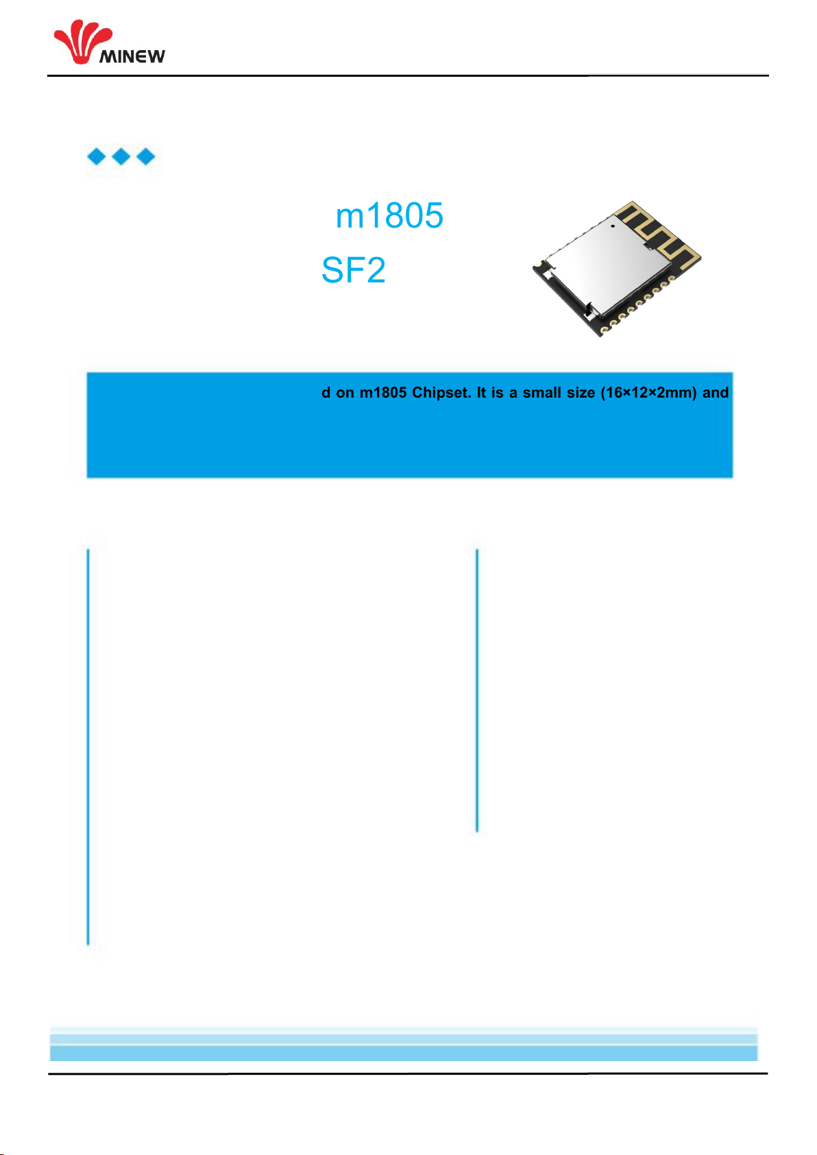
Cost-sensitive m1805
Module MS48SF2
Specification
UART module MS48SF2 is based on m1805 Chipset. It is a small size (16×12×2mm) and
stand-alone module with 12 GPIO. The data transmission between module and mobile
phone can be achieved via operation of UART. With up to 60-meter working distance in
open space, 512KB flash memory, etc., the data can be transmitted via Bluetooth
Applications
Medical devices
Heart rate monitor
Blood pressure monitor
Blood glucose meter
Thermometer
Sport facilities
Weighing machine
Sports and fitness sensors
Accessories
3D glasses and gaming controller
Mobile accessories
Remote controllers / Toys
Electronic devices
Cycle computer
Certification
ISO 9001
ISO14001
OAHS18001
Copyright © Minew
1
Page 2

m1805 Module Specification
Revision history
Version
Date
Notes
Contributor(s)
Person of Approve
V 1.0
2019.02.22
Compiling the specification
Lynn
Copyright © Minew
2
Page 3

m1805 Module Specification
Index
Revision history..........................................................................................................................................................................2
1. Product introduction.............................................................................................................................................................. 4
1.1 Ordering information...................................................................................................................................................4
2. Pin description........................................................................................................................................................................5
2.1 Pin assignment............................................................................................................................................................ 5
2.2 Pin definition.................................................................................................................................................................5
2.3 Block diagram.............................................................................................................................................................. 6
2.4 Mechanical drawing.................................................................................................................................................... 6
3. Electrical specification.......................................................................................................................................................... 7
3.1 Absolute maximum ratings........................................................................................................................................ 7
3.2 Recommended operating conditions.......................................................................................................................8
3.3 Electronic characteristic..........................................................................................................................................8
3.3.1 General radio characteristics.........................................................................................................................8
3.3.2 Radio current consumption (Transmitter).................................................................................................... 8
3.3.3 RX BLE 1Mbps GFSK (Receiver).................................................................................................................9
3.3.4 RX BLE 2Mbps GFSK.....................................................................................................................................9
3.3.5 RX 500kbps GFSK........................................................................................................................................10
3.3.6 RX 125Kbps GFSK........................................................................................................................................11
3.3.7 RSSI Specifications.......................................................................................................................................11
4. Electrical schematic............................................................................................................................................................ 12
5. Package information...........................................................................................................................................................13
5.1 Package dimension.................................................................................................................................................. 13
6. Reflow and soldering.......................................................................................................................................................... 15
7. Notes & cautions................................................................................................................................................................. 16
7.1 Design notes..............................................................................................................................................................16
7.2 Layout notes.............................................................................................................................................................. 16
7.3 Installation and soldering.........................................................................................................................................17
7.4 Handling and storage .............................................................................................................................................17
7.5 Life support applications ........................................................................................................................................18
8. Disclaimer............................................................................................................................................................................. 18
9. Contact information.............................................................................................................................................................19
Copyright © Minew
3
Page 4

m1805 Module Specification
1. Product introduction
Ordering number
Description
MS48SF2
PS1912OB, m1805FA-R, PCB ANT, reel pack
UART module MS48SF2 is based on m1805 Chipset. It is a small size (16×12×2mm) and
stand-alone module with 12 GPIO. The data transmission between module and mobile phone can
be achieved via operation of UART. With up to 60-meter working distance in open space, 512KB
flash memory and -97dBm received sensitivity, the data can be transmitted via Bluetooth.
MS48SF2 is a compact module with a metal cover shield which can support Android 4.3+, IOS 7+.
Its BLE stack can be depth optimization and the transmission speed is up to 3kB/s.
1.1 Ordering information
Copyright © Minew
4
Page 5
m1805 Module Specification
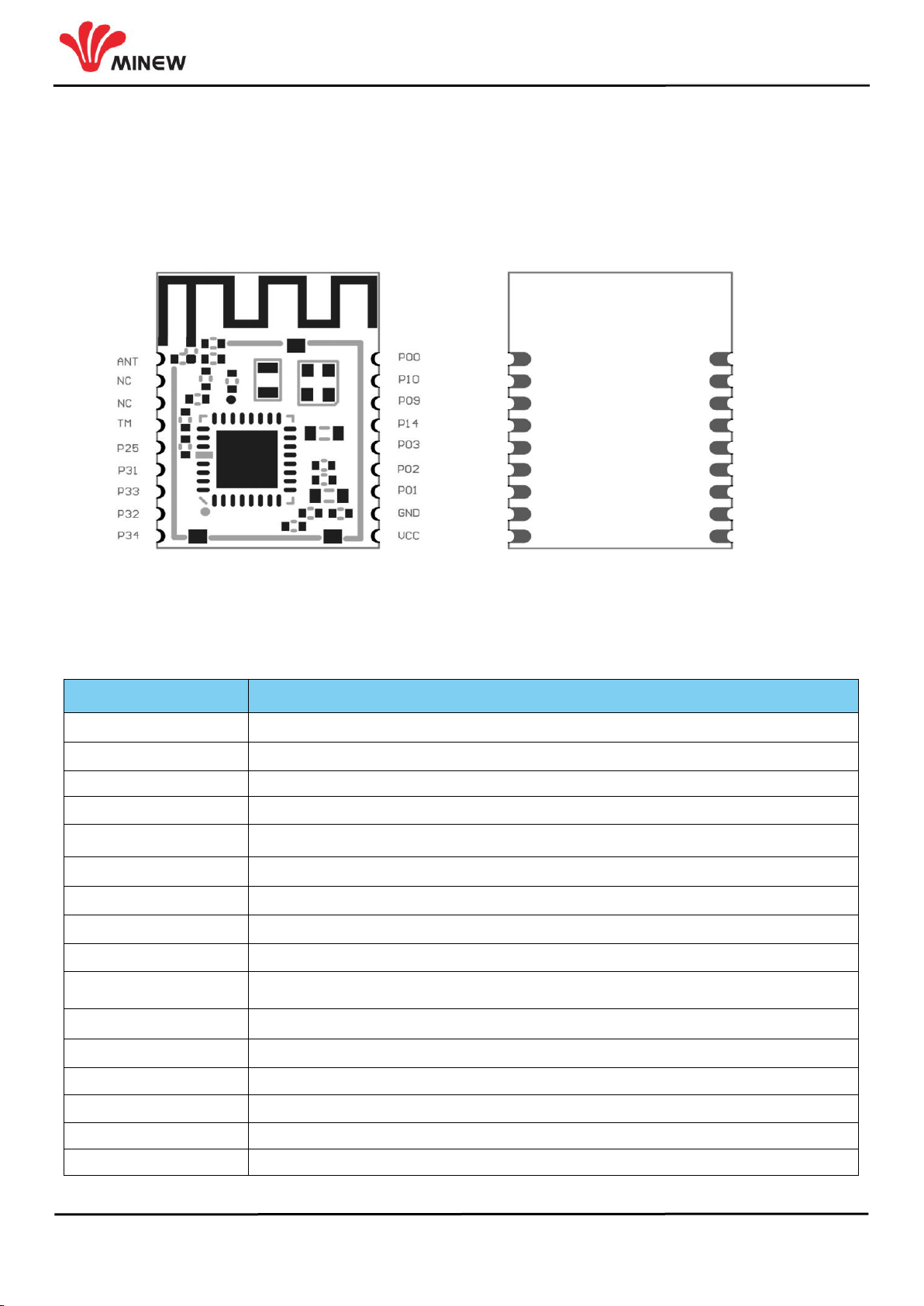
2. Pin description
Symbol
Description
VCC
Power positive pole
GND
Power negative pole
NC
null
ANT
Antenna
P00
All functions configurable/JTAG_TDO(Not support ADC function)
P01
All functions configurable/JTAG_TDI (Not support ADC function)
P02
All functions configurable/JTAG_TMS (Not support ADC function)
P03
All functions configurable/JTAG_TCK (Not support ADC function)
P09
All functions configurable (Not support ADC function)
P10
All functions configurable (Not support ADC function)
P14
All functions configurable/ AIO <3>
P25
All functions configurable/test_mode_select[1](Not suppor interrupt du)
P31
All functions configurable (Not support interrupt and ADC function)
P32
All functions configurable(Not support interrupt and ADC function)
P33
All functions configurable (Not support interrupt and ADC function)
P34
All functions configurable (Not support interrupt and ADC function)
2.1 Pin assignment
2.2 Pin definition
Copyright © Minew
5
Page 6
m1805 Module Specification
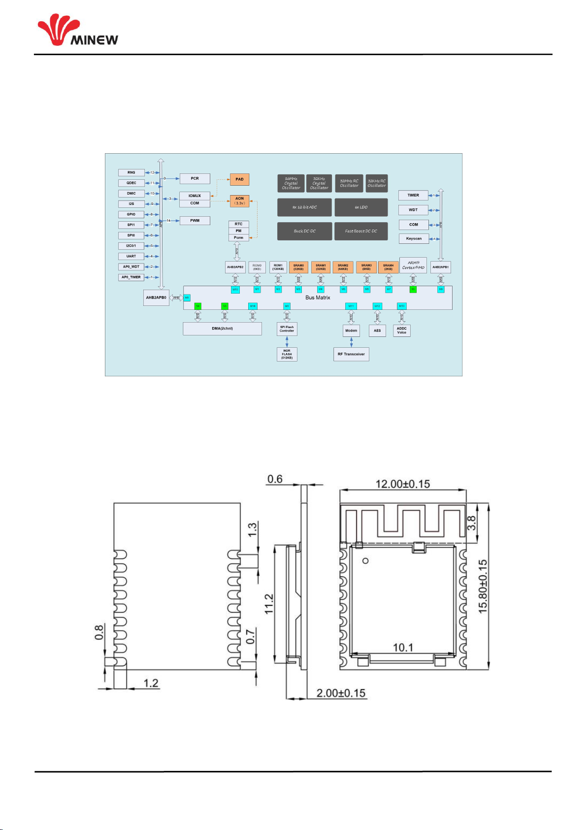
2.3 Block diagram
2.4 Mechanical drawing
Unit: mm
Tolerance: +/- 1.0, default
Copyright © Minew
6
Page 7
m1805 Module Specification
3. Electrical specification
Symbol
Parameter
Min.
Max
Unit
Supply voltages
VDD3
-0.3
+3.6
V
DEC
1.32
V
VSS
0
V
I/O Pin voltage
VIO
-0.3
VDD + 0.3V
V
Environmental (AQFN package)
Storage temperature
-40
+125
°C
MSL
Moisture Sensitivity Level
3
ESD HBM
Human Body Model Class 2
2
KV
ESD CDM
QF
Charged Device Model
500
V
Flash memory
Endurance
20000
Write/erase cycles
Retention
10 years at 40°C
Number of times an
address can be written
between erase cycles
2
Times
The electrical specifications of the module are directly related to the Specifications for the m1805
chipset. The below information is only the extract from m1805 specification. For more detailed
information, please refer to the up-to-date specification of the chipset available.
3.1 Absolute maximum ratings
Notes : Maximum ratings are the extreme limits to which the chip can be exposed for a limited
amount of time without permanently damaging it. Exposure to absolute maximum ratings for
prolonged periods of time may affect the reliability of the device.
Copyright © Minew
7
Page 8

m1805 Module Specification
3.2 Recommended operating conditions
Symbol
Parameter
Min.
Nom.
Max.
Units
VDD3
supply voltage,normal mode
1.8
3.0
3.6
V
tr_VDD
Supply rise time (0 V to 1.8 V)
100
ms
TA
Operating temperature
-4027125
°C
Parameter
Description
Min.
TYP
Max.
Units
Tx only at 0dBm
With internal DC-DC @ 3V
8
mA
Rx only
With internal DC-DC @ 3V
8
mA
Parameter
Description
Min.
Typ.
Max.
Units
RF Max output Power
10
dBm
RF Min Output Power
-20
dBm
OBW for BLE 1Mbps
20dB occupy-bandwidth for BLE modulation 1Mbps
1100
kHz
OBW for BLE 2Mbps
20dB occupy-bandwidth for BLE modulation 2Mbps
2300
kHz
OBW for GFSK 500 kbps
20dB occupy-bandwidth for GFSK modulation 2Mbps
1100
kHz
OBW for GFSK 125 bps
20dB occupy-bandwidth for GFSK modulation 2Mbps
1100
kHz
Error Vector Measure
Offset EVM for OQPSK modulation
0.02
FDEV for BLE 1Mbps
Frequency deviation for GFSK modulation 1Mbps
160
250
kHz
FDEV for BLE 2Mbps
Frequency deviation for GFSK modulation 2Mbps
320
500
kHz
Important : The On-chip power-on reset circuitry may not function properly for rise times longer
than the specified maximum.
3.3 Electronic characteristic
3.3.1 General radio characteristics
3.3.2 Radio current consumption (Transmitter)
Copyright © Minew
8
Page 9
m1805 Module Specification
3.3.3 RX BLE 1Mbps GFSK (Receiver)
Parameter
Description
Min
Typ.
Max.
Units
Rx Sensitivity
Sensitivity test 1Mbps BLE ideal transmitter, 37 Byte
BER=1E-3
-97
dBm
co-channel
rejection
modulated interferer in channel, 37 Byte BER=1E-3
-6
I/C dB
Selectivity +-1MHz
Wanted signal at -67dBm, modulated interferer at +/- 1MHz,
37 Byte BER=1E-3
7
I/C dB
Selectivity +-2MHz
Wanted signal at -67dBm, modulated interferer at +/- 2MHz,
37 Byte BER=1E-3
45
I/C dB
Selectivity +-3MHz
Wanted signal at -67dBm, modulated interferer at +/- 3MHz,
37 Byte BER=1E-3
50
I/C dB
Selectivity +-4MHz
Wanted signal at -67dBm, modulated interferer at +/- 4MHz,
37 Byte BER=1E-3
50
I/C dB
Selectivity +-5MHz
or More
Wanted signal at -67dBm, modulated interferer at >=+/-
5MHz, 37 Byte BER=1E-3
55
I/C dB
Selectivity Imag
frequency
Wanted signal at -67dBm, modulated interferer at
imagefrequency, 37 Byte BER=1E-3
22
I/C dB
Intermodulation
Wanted signal at 2402MHz, -64dBm, Two interferers at 2405
and 2408 MHz respectively, at the given power level, 37 Byte
BER=1E-3
-20
dBm
Carrier Frequency
Offset Tolerance
+-350
KHz
Sample Clock
Offset Tolerance
+-120
ppm
Symbol
Description
Min
Typ.
Max.
Units
Rx Sensitivity
Sensitivity test 2Mbps BLE ideal transmitter, 37 Byte BER=1E-3
-94
dBm
co-channel
rejection
modulated interferer in channel, 37 Byte BER=1E-3
-6
I/C dB
Selectivity +-1MHz
Wanted signal at -67dBm, modulated interferer at +/- 1MHz, 37
Byte BER=1E-3
-5
I/C dB
Selectivity +-2MHz
Wanted signal at -67dBm, modulated interferer at +/- 2MHz, 37
Byte BER=1E-3
9
I/C dB
Selectivity +-3MHz
Wanted signal at -67dBm, modulated interferer at +/- 3MHz, 37
Byte BER=1E-3
30
I/C dB
3.3.4 RX BLE 2Mbps GFSK
Copyright © Minew
9
Page 10

m1805 Module Specification
Selectivity +-4MHz
Wanted signal at -67dBm, modulated interferer at +/- 4MHz, 37
Byte BER=1E-3
40
I/C dB
Selectivity +-5MHz
or More
Wanted signal at -67dBm, modulated interferer at >=+/- 5MHz,
37 Byte BER=1E-3
55
I/C dB
Selectivity Imag
frequency
Wanted signal at -67dBm, modulated interferer at
imagefrequency, 37 Byte BER=1E-3
22
I/C dB
Intermodulation
Wanted signal at 2402MHz, -64dBm, Two interferers at 2405
and 2408 MHz respectively, at the given power level, 37 Byte
BER=1E-3
-20
dBm
Carrier Frequency
Offset Tolerance
+-350
KHz
Sample Clock
Offset Tolerance
+-120
ppm
3.3.5 RX 500kbps GFSK
Parameter
Description
Min
Typ.
Max.
Units
Rx Sensitivity
Sensitivity test 500Kbps BLE ideal transmitter, 37 Byte
BER=1E-3
-98
dBm
co-channel rejection
modulated interferer in channel, 37 Byte BER=1E-3
-4
I/C dB
Selectivity +-1MHz
Wanted signal at -67dBm, modulated interferer at +/- 1MHz,
37 Byte BER=1E-3
10
I/C dB
Selectivity +-2MHz
Wanted signal at -67dBm, modulated interferer at +/- 2MHz,
37 Byte BER=1E-3
45
I/C dB
Selectivity +-3MHz
Wanted signal at -67dBm, modulated interferer at +/- 3MHz,
37 Byte BER=1E-3
50
I/C dB
Selectivity +-4MHz
Wanted signal at -67dBm, modulated interferer at +/- 4MHz,
37 Byte BER=1E-3
50
I/C dB
Selectivity +-5MHz or
More
Wanted signal at -67dBm, modulated interferer at >=+/-
5MHz, 37 Byte BER=1E-3
55
I/C dB
Selectivity Imag
frequency
Wanted signal at -67dBm, modulated interferer at
imagefrequency, 37 Byte BER=1E-3
24
I/C dB
Intermodulation
Wanted signal at 2402MHz, -64dBm, Two interferers at 2405
and 2408 MHz respectively, at the given power level, 37 Byte
Ber=1E-3
-19
dBm
Carrier Frequency
Offset Tolerance
+-350
KHz
Sample Clock Offset
Tolerance
+-120
ppm
Copyright © Minew
10
Page 11

m1805 Module Specification
3.3.6 RX 125Kbps GFSK
Parameter
Description
Min
Typ.
Max.
Units
Rx Sensitivity
Sensitivity test 125Kbps BLE ideal transmitter, 37 Byte
BER=1E-3
-103
dBm
co-channel
rejection
modulated interferer in channel, 37 Byte BER=1E-3
-1
I/C dB
Selectivity +-1MHz
Wanted signal at -67dBm, modulated interferer at +/- 1MHz, 37
Byte BER=1E-3
-11
I/C dB
Selectivity +-2MHz
Wanted signal at -67dBm, modulated interferer at +/- 2MHz, 37
Byte BER=1E-3
45
I/C dB
Selectivity +-3MHz
Wanted signal at -67dBm, modulated interferer at +/- 3MHz, 37
Byte BER=1E-3
50
I/C dB
Selectivity +-4MHz
Wanted signal at -67dBm, modulated interferer at +/- 4MHz, 37
Byte BER=1E-3
50
I/C dB
Selectivity +-5MHz
or More
Wanted signal at -67dBm, modulated interferer at >=+/- 5MHz,
37 Byte BER=1E-3
55
I/C dB
Selectivity Imag
frequency
Wanted signal at -67dBm, modulated interferer at image
frequency, 37 Byte BER=1E-3
28
I/C dB
Intermodulation
Wanted signal at 2402MHz, -64dBm, Two interferers at 2405
and 2408 MHz respectively, at the given power level, 37 Byte
BER=1E-3
-18
dBm
Carrier Frequency
Offset Tolerance
+-350
KHz
Sample Clock
Offset Tolerance
+-120
ppm
Parameter
Description
Min
Typ.
Max.
Units
RSSI Dynamic Range
70
dB
RSSI Accuracy
RSSI Accuracy Valid in range -100 to -30dBm
+/-2
dB
RSSI Resolution
Totally 7bit, from 0 to 127
1
dB
RSSI Period
8
us
3.3.7 RSSI Specifications
Copyright © Minew
11
Page 12

m1805 Module Specification
4. Electrical schematic
Copyright © Minew
12
Page 13

m1805 Module Specification
5. Package information
Unit: mm
Tolerance: +/- 0.1, default
5.1 Package dimension
Copyright © Minew
13
Page 14

m1805 Module Specification
Unit: mm
Tolerance: +/- 0.1, default
Details
Reel
Quantity(module)
850PCS
Tape Weight
450g
Single module Weight
0.6g
Gross Weight
970g
Dimension
W:44mm T:0.35mm
Tolerance: +/- 10g, default
Copyright © Minew
14
Page 15

m1805 Module Specification
6. Reflow and soldering
Profile Feature
Sn-Pb Assembly
Pb-Free Assembly
Solder Paste
Sn63/Pb37
Sn96.5/Ag3/Cu0.5
Preheat Temperature min (Tsmin)
100°C
150°C
Preheat Temperature max (Tsmax)
150°C
200°C
Preheat Time (Tsmin to Tsmax)(ts)
60-120 sec
60-120 sec
Average ramp-up rate (Tsmax to Tp)
3°C/second max
3°C/second max
Liquidous Temperature (TL)
183°C
217°C
Time (tL)Maintained Above (TL)
60-90 sec
30-90 sec
Peak Temperature (Tp)
220-235°C
230-250°C
Average ramp-down rate (Tp to Tsmax)
6°C/second max
6°C/second max
Time 25°C to peak temperature
6 minutes max
8 minutes max
Copyright © Minew
15
Page 16

m1805 Module Specification
7. Notes & cautions
We cannot assure that the specification has no errors and omission even though this specification
is under collate and check strictly.
This specification is under the protection of laws and regulations of copyright, please do not copy
and duplicate at any form, or do not transmit part or full of this specification in any wire and wireless
network in any form, or do not edit or translate to any other format, word, code, etc.
7.1 Design notes
(1) It is critical to following the recommendations of this document to ensure the module meets
the specifications.
(2) The module should be placed at the edge of the circuit board as far as possible to keep away
from other circuits.
(3) Antenna should be kept away from other circuits. It can prevent low radiation efficiency and
the normal use of other circuits from being affected.
(4) The landing of components should be appropriate and that is better for reducing the parasitic
inductance.
(5) Please refuse to supply voltage that is not within the range of specification.
(6) Please make sure the module or its surface may not suffer from the physical shock or
extreme stress.
7.2 Layout notes
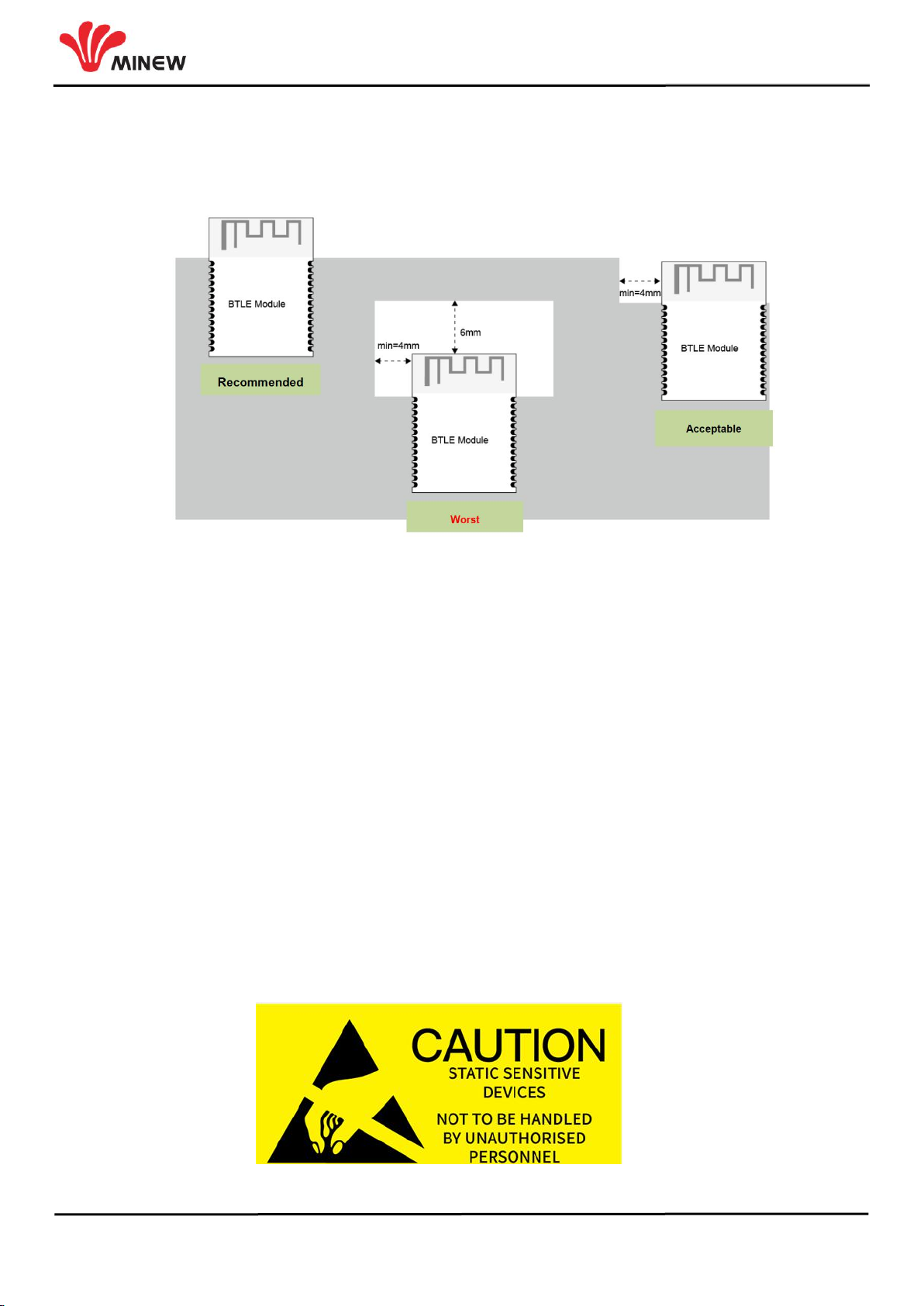
To make sure wireless performance is at its best condition, please layout the module on the carrier
board as below instructions and picture.
(1) Placement of the antenna
The antenna area of module shall lay clearance completely and should not be blocked by the metal.
Otherwise it will have effect on antenna performance (As the picture indicated below).
(2) Placement of top-layer
The placement of top-layer in carrier board shall be lay copper completely to reduce the signal line
in carrier board or other interference.
(3) Clearance
Copyright © Minew
16
Page 17
m1805 Module Specification
The upper and below area of antenna (including the case) shall have 4mm or more than 4mm
clearance to reduce the influences for antenna.
*The Grey area above is Carrier board.
7.3 Installation and soldering
(1) Please do not lay copper under the module antenna. It can prevent the influence of signal
radiation and the transmission distance from being affected.
7.4 Handling and storage
(1) Due to the fact that CMOS components are included in the module, it is better to eliminate
static electricity at any methods when transporting or working with the module. Moreover, it is
strongly recommended adding anti-ESD components to circuit design to hinder damage from
real-life ESD events. Anti-ESD methods can be also used in mechanical design.
Copyright © Minew
17
Page 18

m1805 Module Specification
(2) Please store the modules within -40℃to +125℃before and after installation and make sure
the modules is away from the direct sunlight exposure for a long duration. Modules should be far
away from humid and salty air conditions, and any corrosive gasses or substances.
(3) Please not to wash the module. No-Clean Paste is used in production. The metal shield may
be oxidized by the washing process and may lead to chemistry reaction with No-Clean Paste. If
modules goes through the washing process, functions of the module may not guaranteed.
7.5 Life support applications
(1) The module is not design for life support device or system and not allowed to be used in
destructive devices or system in any direct, or indirect ways. Minew is not responsible for
compensation of any losses when applying modules under such application as described above.
(2) Minew shall not responsible for the customer’s products or application.
8. Disclaimer
The factory has passed the ISO9001 quality management system, ISO14001 environmental
management system and OAHS18001 occupational health and safety assessment . Each product
has been rigorously tested (transmission power test, sensitivity test, power consumption test,
stability test, aging test, etc.).
* NOTICES:
(1) The Bluetooth trade mark is owned by the Bluetooth SIG Inc. USA.
(2) All other trademarks listed herein are owned by their respective owners.
(3) All specifications are subject to change without notice.
(4) Please do not use this specification for produce, sell or illegal purpose without Minew’s
authorization.
(5) Minew have right to interpret all the items above.
Copyright © Minew
18
Page 19

m1805 Module Specification
9. Contact information
Manufacturer: Shenzhen Minew Technologies Co., Ltd.
Tel: 0086-755-2103 8160
Email: info@Minew.com
URL: https://www.minew.com/
Address:
3rdFloor, Building I,
Gangzhilong Science Park,
Qinglong Road, Longhua District,
Shenzhen 518109,
China
Copyright © Minew
19
Page 20

FCC WARNING
This device complies with part 15 of the FCC Rules. Operation is subject to the following two
conditions: (1) this device may not cause harmful interference, and (2) this device must accept
any interference received, including interference that may cause undesired operation.
Any changes or modifications not expressly approved by the party responsible for compliance
could void the user's authority to operate the equipment.
NOTE: This equipment has been tested and found to comply with the limits for a Class B
digital device, pursuant to Part 15 of the FCC Rules. These limits are designed to provide
reasonable protection against harmful interference in a residential installation. This equipment
generates, uses and can radiate radio frequency energy and, if not installed and used in
accordance with the instructions, may cause harmful interference to radio communications.
However, there is no guarantee that interference will not occur in a particular installation.
If this equipment does cause harmful interference to radio or television reception,
which can be determined by turning the equipment off and on, the user is encouraged to try to
correct the interference by one or more of the following measures:
-- Reorient or relocate the receiving antenna.
-- Increase the separation between the equipment and receiver.
-- Connect the equipment into an outlet on a circuit different
from that to which the receiver is connected.
-- Consult the dealer or an experienced radio/TV technician for help.
The device has been evaluated to meet general RF exposure requirement. The device can be used in
portable exposure condition without restriction.
This module meets the requirements of FCC part 15C(15.247).it specifically establish the 6dB Bandwidth,
Peak Output Power, Radiated Spurious Emission, Power Spectral Density, Restricted Band of Operation
and Band Edge, Out of Band Emissions. It is a single module. PCB antenna, antenna gain
tolerance:-2.48dBi ± 0.5
The antenna cannot be removed , Unconventional interface, The module with trace antenna designs, and
This manual has been shown the layout of trace design, antenna, connectors, and isolation
requirements.
This module It’s complies with FCC RF radiation exposure limits set forth for an uncontrolled environment.
This module is designed to comply with the FCC
statement, FCC ID is: 2ABU6-MS48SF2.
The host system using this module, should have label in a visible area indicated the following texts:
"Contains FCC ID: 2ABU6-MS48SF2.
SHENZHEN MINEW TECHNOLOGIES CO., LTD. can increase the utility of our modular transmitters by
providing instructions that simulates or characterizes a connection by enabling a transmitter.
The module without unintentional-radiator digital circuity, so the module does not require an evaluation
by FCC Part 15 Subpart B. The host shoule be evaluated by the FCC Subpart B.
 Loading...