


MC13xx
High Speed CMOS Camera
Mikrotron GmbH
Landshuter Str. 20-22
D-85716 Unterschleißheim
Germany
Tel.: +49 89 726342 00
Fax: +49 89 726342 99
info@mikrotron.de
www.mikrotron.de
MC13xx Users Manual Rev. 1.19
Camera-Firmware:
V1.51-F2.53
Kamera ID Nr.: MC1302 .. MC1319
Copyright © 2006 Mikrotron GmbH

General MC13xx Users Manual Rev. 1.19
2
Table of contents
1 General..........................................................................................................................4
1.1 For customers in the U.S.A. .................................................................................................................................... 4
1.2 For customers in Canada......................................................................................................................................... 4
1.3 Pour utilisateurs au Canada ..................................................................................................................................... 4
1.4 Life Support Applications ....................................................................................................................................... 4
1.5 Declaration of conformity ....................................................................................................................................... 5
1.6 Warranty Note......................................................................................................................................................... 6
1.7 Remarks, Warnings................................................................................................................................................. 6
2 Introduction...................................................................................................................7
2.1 Top level specifications........................................................................................................................................... 7
2.2 Electronic „Freeze Frame“ Shutter.......................................................................................................................... 7
2.3 Differences between the camera types .................................................................................................................... 8
2.4 Using the camera..................................................................................................................................................... 8
3 Hardware.......................................................................................................................9
3.1 Camera Link® Interface.......................................................................................................................................... 9
3.1.1 Serial interface.................................................................................................................................................... 9
3.2 Power supply........................................................................................................................................................... 9
3.3 Status LED .............................................................................................................................................................. 9
4 Getting started.............................................................................................................10
4.1 First steps .............................................................................................................................................................. 10
5 Initial setup .................................................................................................................11
5.1 Serial number and firmware revision .................................................................................................................... 11
5.2 PowerUpProfile..................................................................................................................................................... 11
5.3 Camera Profile ...................................................................................................................................................... 11
5.4 Factory profile....................................................................................................................................................... 11
5.5 User profiles .......................................................................................................................................................... 11
6 Configuration..............................................................................................................12
6.1 Commands............................................................................................................................................................. 12
6.1.1 Table of commands .......................................................................................................................................... 13
6.2 Read serial number and firmware revision............................................................................................................ 13
6.2.1 Read camera settings ........................................................................................................................................ 13
6.3 Profile processing.................................................................................................................................................. 15
6.3.1 Read Camera profile......................................................................................................................................... 15
6.3.2 Write user profile.............................................................................................................................................. 15
6.3.3 Load user profile .............................................................................................................................................. 16
6.3.4 Load factory profile.......................................................................................................................................... 16
6.4 Video data width, Base/ Full Camera Link® ........................................................................................................ 16
6.5 Image quality......................................................................................................................................................... 16
6.5.1 FPN................................................................................................................................................................... 16
6.5.2 Gain .................................................................................................................................................................. 17
6.5.3 Black Level....................................................................................................................................................... 17
6.6 Image size and position ......................................................................................................................................... 17
6.6.1 Address of the first line .................................................................................................................................... 17
6.6.2 Number of lines ................................................................................................................................................ 17
6.6.3 Address of the first pixel of a line .................................................................................................................... 18
6.6.4 Address of the last pixel of a line ..................................................................................................................... 18
6.6.5 Tracking ........................................................................................................................................................... 18
6.6.6 Arbitrary shaped fields of view ........................................................................................................................ 18
6.7 Clock selection...................................................................................................................................................... 20
6.7.1 Arbitrary selection of sensor and pixel clock ................................................................................................... 20
6.7.2 Table selection of clock frequencies................................................................................................................. 20
6.7.3 Image Format/Speed change ............................................................................................................................ 21
6.8 Exposure control ................................................................................................................................................... 21
6.8.1 Type of exposure.............................................................................................................................................. 21
6.8.2 Frame rate with synchronous exposure ............................................................................................................ 22

General MC13xx Users Manual Rev. 1.19
3
6.8.3 Synchronous operation without shutter ............................................................................................................ 23
6.8.4 Synchronous operation with shutter ................................................................................................................. 23
6.8.5 External synchronisation with synchronous exposure ...................................................................................... 23
6.8.6 Frame rate with asynchronous exposure........................................................................................................... 24
6.8.7 Asynchronous exposure, shutter control by pulse width.................................................................................. 24
6.8.8 Asynchronous exposure, shutter control by timer ............................................................................................ 24
6.9 Firmware ............................................................................................................................................................... 25
6.9.1 Update Firmware.............................................................................................................................................. 25
6.9.2 Reset and configuration of the internal FPGA.................................................................................................. 25
6.10 Horizontal pixelbinning......................................................................................................................................... 25
6.11 Vertical pixelbinning............................................................................................................................................. 25
6.12 Digital shading correction ..................................................................................................................................... 26
6.13 Digital gain............................................................................................................................................................ 26
6.14 External clock input .............................................................................................................................................. 26
6.15 Polarity of EXP-signal .......................................................................................................................................... 26
6.16 Test image ............................................................................................................................................................. 27
6.17 Image counter........................................................................................................................................................ 27
6.18 ImageBLITZ® shutter release, MC131x only ...................................................................................................... 27
6.18.1 ImageBLITZ® processing........................................................................................................................... 28
6.18.2 ImageBLITZ® programming ...................................................................................................................... 28
6.18.3 ImageBLITZ® registers .............................................................................................................................. 30
6.18.4 ImageBLITZ® setup.................................................................................................................................... 31
7 MC13xx configuration tool ........................................................................................32
7.1 Basic Configuration............................................................................................................................................... 32
7.2 ImageBLITZ® Configuration ............................................................................................................................... 33
8 Mechanical dimensions ..............................................................................................34
8.1 Camera body MC13xx .......................................................................................................................................... 34
8.1.1 Dimensioned drawing, side view of MC1302/03/10/11................................................................................... 34
8.1.2 Dimensioned drawing, side view of MC13x6 – MC13x9................................................................................ 34
8.1.3 Dimensioned drawing, front view of MC1302/03/10/11.................................................................................. 35
8.1.4 Dimensioned drawing, rear view of MC13xx .................................................................................................. 35
8.2 Lens adjustment .................................................................................................................................................... 36
8.2.1 Lens adaption ................................................................................................................................................... 36
8.2.2 Adjustable lens adapter, only for camera models with C-mount flange ........................................................... 36
8.2.3 Lens selection for camera types with C-mount flange (see table overview of cameras) .................................. 36
9 Technical Data............................................................................................................37
9.1 Spectral response................................................................................................................................................... 38
9.2 Sensitive area of a pixel ........................................................................................................................................ 39
9.3 Connector pinning ................................................................................................................................................. 40
9.3.1 Camera Link® Connector, MDR-26 ................................................................................................................ 40
9.3.2 Circular power connector, 6-pin....................................................................................................................... 41
9.4 Camera Link® Bit Assignments ........................................................................................................................... 42
9.4.1 Base Camera Link® 2*8/10 - Bit Assignment ................................................................................................. 42
9.4.2 Full Camera Link® 8*8-Bit Assignment.......................................................................................................... 43
9.4.3 10*8-Bit Assignment........................................................................................................................................ 44
9.5 Frequency selection............................................................................................................................................... 45
9.5.1 Frequencies for video data width 2*8/10 - Bit, Base Camera Link®............................................................... 45
9.5.2 Frequencies for video data width 8*8 - Bit, Full Camera Link® ..................................................................... 49
9.5.3 Frequencies for video data width 10*8 – Bit.................................................................................................... 49
9.6 Programming sequence, factory profile f3 ............................................................................................................ 50
9.7 Timing................................................................................................................................................................... 51
9.7.1 Pixel clock ........................................................................................................................................................ 51
9.7.2 Line Valid (LVAL, DVAL).............................................................................................................................. 51
9.7.3 Frame Valid (FVAL)........................................................................................................................................ 52
9.7.4 Exposure Signal EXP, to be input on CC1....................................................................................................... 52
9.7.5 Synchronous exposure with external synchronisation via CC1........................................................................ 53

General MC13xx Users Manual Rev. 1.19
4
1 General
1.1 For customers in the U.S.A.
This equipment has been tested and found to comply with the limits for a Class A digital device, pursuant to Part 15 of the FCC Rules. These limits are designed to provide reasonable protection against
harmful interference when the equipment is operated in a commercial environment. This equipment
generates, uses, and can radiate radio frequency energy and, if not installed and used in accordance with
the instruction manual, may cause harmful interference to radio communications. Operation of this
equipment in a residential area is likely to cause harmful interference in which case the user will be required to correct the interference at his own expense. You are cautioned that any changes or modifications not expressly approved in this manual could void your authority to operate this equipment. The
shielded interface cable recommended in this manual must be used with this equipment in order to
comply with the limits for a computing device pursuant to Subpart J of Part 15 of FCC Rules.
1.2 For customers in Canada
This apparatus complies with the Class A limits for radio noise emissions set out in Radio Interference
Regulations.
1.3 Pour utilisateurs au Canada
Cet appareil est conforme aux normes Classe A pour bruits radioélectriques, spécifiées dans le Règlement sur le brouillage radioélectrique.
1.4 Life Support Applications
These products are not designed for use in life support appliances, devices, or systems where malfunction of these products can reasonably be expected to result in personal injury. Mikrotron customers using or selling these products for use in such applications do so at their own risk and agree to fully indemnify Mikrotron for any damages resulting from such improper use or sale.

General MC13xx Users Manual Rev. 1.19
5
1.5 Declaration of conformity
Manufacturer: Mikrotron GmbH
Address: Landshuter Str. 20-22
85716 Unterschleissheim
Deutschland
Product: camera MC1302, MC1303, MC1304, MC1305
camera MC1306, MC1307, MC1308, MC1309
camera MC1310, MC1311, MC1314, MC1315
camera MC1316, MC1317, MC1318, MC1319
The dedicated products conform to the requirements of the Council Directives 2004/108/EG for the
approximation of the laws of the Member States relating to electromagnetic consistency. The following
standards were consulted for the conformity testing with regard to electromagnetic consistency.
EC regulation Description
EN 61000-6-3 Electromagnetic compatibility
EN 61000-6-1 Immunity
Unterschleissheim, June 06
th
. 2003
Mikrotron GmbH
Dipl.-Ing. Bernhard Mindermann
President of Mikrotron

General MC13xx Users Manual Rev. 1.19
6
1.6 Warranty Note
Do not open the body of the camera. The warranty becomes void if the body is opened.
1.7 Remarks, Warnings
This document contains important remarks and warnings. See the corresponding symbols:
L
Important remark
*
Attention, Warning

Introduction MC13xx Users Manual Rev. 1.19
7
2 Introduction
The CMOS high speed camera MC13xx is a high resolution camera with 1280•1024 pixel. Benefits of
CMOS technology are high speed, random access to pixels with free programmability and low power.
The camera uses industry-standard C-Mount lenses. The sensor diagonal is 1,25“ with square pixels
measuring 12µm.
Free programmability means that the user is free to define the region of interest by size and position and
the speed of data output. The frame rate can be selected between 25 fps and several thousand fps
depending on resolution and video data width.
With a resolution of 1280 x 1024 pixel, 500 fps (MC131x) can be output via the “full Camera Link®
parameter sets are called: profiles and stored in non volatile memory.
2.1 Top level specifications
• high resolution: 1.280•1.024 pixel CMOS sensor
with 1300 A/D converters
• up to 1.024 gray levels
• up to 100 full frames/s for MC1302 – MC1309
up to 500 full frames/s for MC1310 – MC1319
• arbitrary region of interest
• high sensitivity
• 12μm square pixels
• electronic “Freeze Frame” shutter
• low blooming
• programmable via serial link
• patented ImageBLITZ® image trigger (MC1310 – MC1319)
• asynchronous trigger
• download customer specific FPGA preprocessing firmware
• small, compact housing
• wide power supply range
2.2 Electronic „Freeze Frame“ Shutter
Preceding exposure, the contents of all light sensitive elements is cleared. When exposure terminates,
accumulated charge is transferred to an analog memory associated which each pixel. It stays there until
it is read out (and discharged) by the A/D conversion cycle.
As all light sensitive elements are exposed at the same time, even fast moving objects are captured
without geometric distortion.

Introduction MC13xx Users Manual Rev. 1.19
2.3 Differences between the camera types
The CMOS cameras are available in different versions depending on the supported features monochrome/color or Base/Full Camera Link ® interface, lens connection to C-mount or changeable lens
adapter C-mount/F-mount.
Features
Type
Data
width
(bits)
Color/
Mono
Base/Full
Camera Link® no. of taps
C/F-Mount
lens adaption
max. frame rate@
1280 x 1024
ImageBLITZ®
Image preprocessing
supported
MC1302 8/10 M B-2 C 100 fps - MC1303 8/10 C B-2 C 100 fps - MC1304 8/10 M B-2 C 100 fps - +
MC1305 8/10 C B-2 C 100 fps - +
MC1306 8/10 M B-2 F 100 fps - +
MC1307 8/10 C B-2 F 100 fps - +
MC1308 8/10 M B-2 F 100 fps - MC1309 8/10 M B-2 F 100 fps - MC1310 8/10 M B,F-2,8,10 C 500 fps + MC1311 8/10 C B,F-2,8,10 C 500 fps + MC1314 8/10 M B,F-2,8,10 C 500 fps + +
MC1315 8/10 C B,F-2,8,10 C 500 fps + +
MC1316 8/10 M B,F-2,8,10 F 500 fps + +
MC1317 8/10 C B,F-2,8,10 F 500 fps + +
MC1318 8/10 M B,F-2,8,10 F 500 fps + MC1319 8/10 C B,F-2,8,10 F 500 fps + -
Table 2.3-1
+ ... supported
- ... not supported
2.4 Using the camera
There are no serviceable parts inside the camera.. The camera may not be opened, otherwise guarantee
is lost.
Use dry, soft lens-cleaning tissue for cleaning lenses and, if necessary, the sensors window.
8

Hardware MC13xx Users Manual Rev. 1.19
9
3 Hardware
3.1 Camera Link® Interface
Camera Link® is designed for digital cameras in machine vision applications. A “Full Camera Link®”
interface can transfer up to 64 bits of data at a rate of >528 Mbytes/sec.
3.1.1 Serial interface
The communication via the serial interface is incorporated in the “Base Camera Link® interface. A description of the connector pinning is in chapter 9.3.
3.2 Power supply
The camera needs a DC supply voltage between 8 … 24 V at a power consumption of 6,0 Watt max..
See also Connector pinning .
*
Before applying power to the camera we strongly recommend to verify the used pins of the
power connector, the polarity (+/-) of the leads and the supply voltage.
The camera may only be used with a supply voltage according to the camera specification.
Connecting a lower or higher supply voltage, AC voltage, reversal polarity or using wrong
pins of the power connector may damage the camera. If doing so, the warranty will expire
immediately.
3.3 Status LED
A dual colour LED on the camera backplane shows the operating condition of the MC13xx.
LED orange... The MC13xx is configuring the internal FPGA. No other activity is possible.
LED green... The MC13xx is fully operational.
LED off... If LED is off, despite the camera is powered, the FPGA configuration data is re-
loaded via the serial interface and stored in internal EEPROM. No other activity
is possible.
LED red... red LED that the FPGA could not be loaded because of wrong FPGA configura-
tion data. Try to reload configuration data.

Getting started MC13xx Users Manual Rev. 1.19
10
4 Getting started
Before starting to operate the camera, make sure that the following equipment is available:
• Camera MC13xx
• C-Mount Lens
• Mikrotron Support CD
• Image processing system, e.g.: PC, frame grabber and Software
L
The frame grabber must have a Base- or Full Camera
Link® Interface.
Additional items:
• 1 or 2 standard Camera Link® cables
• 1 Power supply 12VDC, 0.5A min
• 1 power cable
L
To specify cables see chapter Connector pinning.
4.1 First steps
1. Switch off the image processing system
2. Connect Camera Link® cable between camera and frame grabber.
3. Connect power cable.
4. Unscrew dust protection cover, screw in lens.
5. Switch on the image processing system and camera power supply

Initial setup MC13xx Users Manual Rev. 1.19
11
5 Initial setup
The MC13xx is delivered with initial parameters and therefore does not need to be configured via the
serial link.
5.1 Serial number and firmware revision
Serial number and firmware revision is provided in MC13xx non volatile memory. Use :v command
(Read serial number and firmware revision) to read serial number and firmware revision. The serial
number is also marked on the type plate of the camera.
5.2 PowerUpProfile
The PowerUpProfile is the contents of all camera registers to be loaded from non-volatile memory after
power up.
5.3 Camera Profile
The actual set of parameters is called Camera Profile. All changes of parameters by the serial link is
reflected in the Camera Profile. On command the Camera Profile is saved to 8 user profiles or one PowerUpProfile. It is loaded from 8 user profiles or 8 factory profiles or the PowerUpProfile. The camera
profile is volatile and must be stored to the PowerUpProfile to be reactivated on next poer up.
5.4 Factory profile
The factory profile can be read but not written by the user.
5.5 User profiles
The user can store up to eight PowerUpProfiles in non volatile memory. All load or write commands
exchange data between the PowerUpProfile and one of the four user profiles.
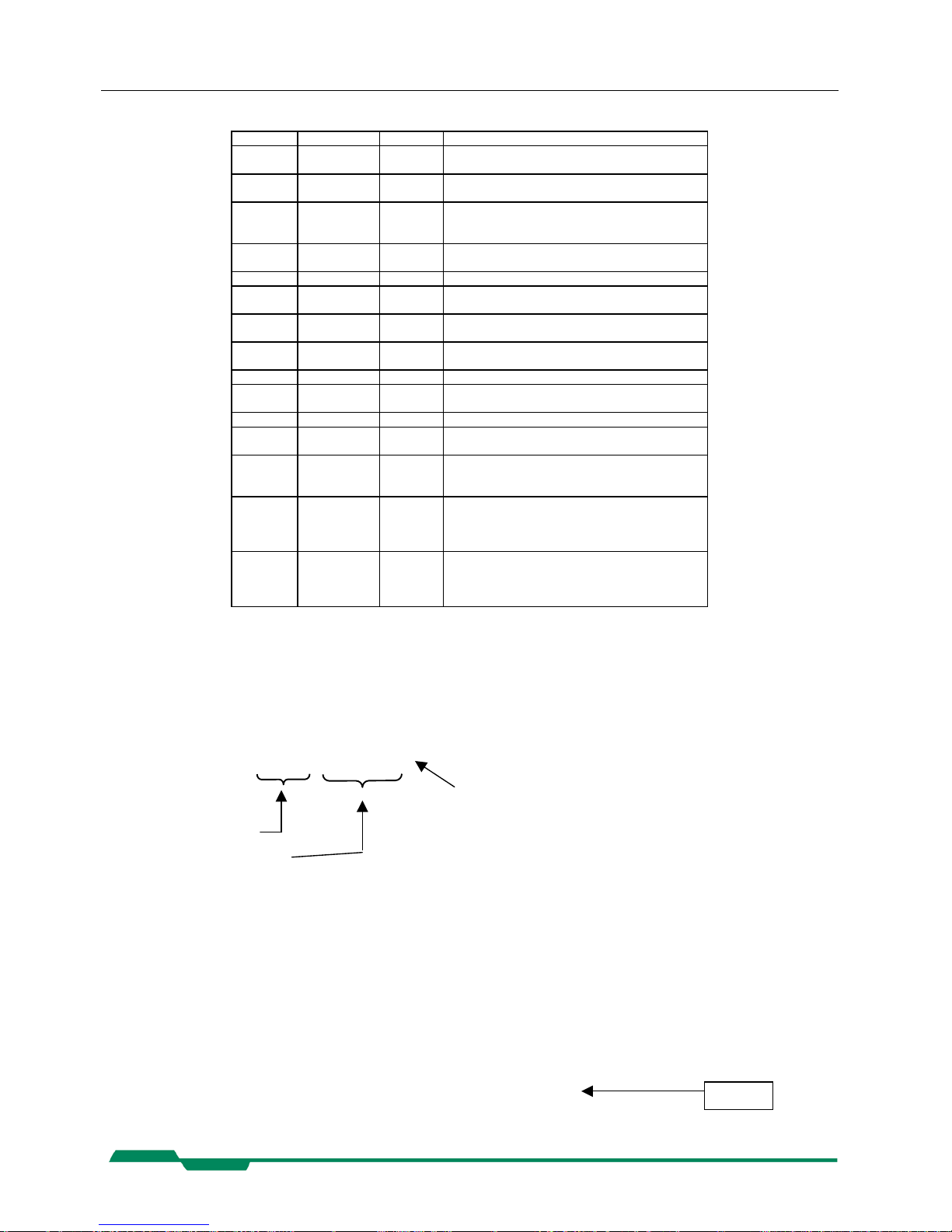
Profil-Nr. Video data
width
resolution
/ pixel
Image
frequency
/fps
0 2x8 100 x 100 4.852
1 2x8 240 x 240 1.011
2 2x8 640 x 480 202
3 2x8 1280 x 1024 47
4 2x10 640 x 480 156
5 2x10 1280 x 1024 32
6 8x8 1280 x 1024 120
7 8x8 640 x 480 954
Table 5-1

Configuration MC13xx Users Manual Rev. 1.19
12
6 Configuration
The MC13xx has 15 FPGA registers, r1..rfh , each 10 bit wide, eight D/A registers, a1..a8, 8-bit wide,
and one clock select register, 4 bit wide. The contents of all the above registers is called a profile. There
is space in non volatile memory for 17 profiles: one PowerUpProfile, 8 user profiles and 8 factory profiles.
Any change of a specific register through the serial interface is immediately processed and written to
the volatile part of the memory and gets lost when power goes down. A command must be used to store
the actual setting in non volatile memory. After power-up the PowerUpProfile is loaded from the nonvolatile to the volatile part of the memory.
A load or write command exchanges data between the PowerUpProfile and one of the eight user profiles. The eight factory profiles can be read but not be written by any command. All values are given in
hexadecimal notation, e.g.: 0xff or 0ffh = 255.
6.1 Commands
ASCII strings are used to change camera parameters. All commands start with a colon, followed by one
selection character and a value in hexadecimal notation with two or three ASCII characters.
After a command has been recognized, processing is immediate, for all commands but the save type
commands (:px). These need a EEPROM write time of app 1ms. An answer is provided with read type
commans (:v, :w, :W) or, if the command “command acknowledge flag” is set, after processing of each
command an ACK or NAK character. Processing of wrong command is stopped immediately on recognizing the error. A new command must start with a colon.
Configuration MC13xx Users Manual Rev. 1.19
6.1.1 Table of commands
Syntax Range Answer Description
:a<n><xx> <n> = 1...8
<xx> = 0...ff
h
-- Set one of eight analog voltages for the sensor
:A<n> <n> =
„y“,“Y“,“n“,“N“
En- or disable a command acknowledge or not
acknowledge (ACK or NAK)
:b<n> <n> = 0...4 -- Select baud rate:
0=9600 Bd (default setting), 1=19.2 kBd,
2=38.4 kBd, 3=56.8 kBd, 4=115.2 kBd
:c -- -- RESET and new Initialization of the camera, new
load of PowerUpProfile. Duration: some seconds
:e... -- -- Transmit & save a new FPGA configuration
:f<n> <n> = 0...7 -- Reload one of eight, factory defined and cali-
brated profiles to PowerUpProfile.
:g<n> <n> = 0...7 -- Reload one of eight user profiles to PowerUp-
Profile
:p<n> <n> = 0...7 -- Save PowerUpProfile to one of eight user pro-
files, allow app. 1ms save time.
:r<n> <n> = 1...f
h
-- Write a FPGA - register
:s<n> <n> = 0…f
h
-- Select sensor and pixel clock from a table with
16 entries.
:S 6 Byte Code -- Program sensor and pixel clock directly.
:t<n><m> <n> = 00..7f
h
<m> = 00..ff
h
-- Short setting of X- position in units of 10 pixel
and Y-position in units of 4 lines.
:v -- #12345-
V1.10F1.29
Read serial number (#), microcontroller - version
(V...) and FPGA - version (F...).
:w -- camera
profile: 44
bytes in
hex
Read actual PowerUpProfile, data output in hex
:W -- Camera
profile: 44
bytes in
ASCII
Read actual PowerUpProfile, data output in
ASCII
6.2 Read serial number and firmware revision
The serial number and the firmware revision can be read with the :v command.
Command: :v
Response(e.g.): #01234-V1.51-F2.53↵
CR+LF
Serial number (carriage return +
of the camera line feed)
firmware version
6.2.1 Read camera settings
The actual camera settings can be read out. The answer are the values of all camera registers.
Command: :w Output as hexadecimal digits
(44 Bytes)
:W Output as ASCII-String
Example for ":w" (output as hex digits, 44 Databytes + CR + LF):
6d6448c66500650061008541898c0000
03f f03f f0000007f 0030000000000000
000000000000000000000000↵
CR+LF
13
Configuration MC13xx Users Manual Rev. 1.19
Example for ":W" (output as ASCII string, 91 Bytes total, 88 databytes, 1x CR preceding the databytes,
1x CR after 32 ASCII-characters and 1x CR after 64 ASCII- characters):
↓6d6448c66500650061008541898c0000↓
03f f03f f0000007f 0030000000000000↓
CR
000000000000000000000000
Assignment of data to camera parameters:
6d6448c665006500 61008541898c 0000
03f f03f f0000007f 0030000000000000
000000000000000000000000↵
14
transmitted bytes:
A1 A2 A3 A4 A5 A6 A7 A8 Sa1 Sa2 Sa3 Sb1 Sb2 Sb3
R1h R1l ... R15h R15l↵
A1...A8 analog settings
Sa1 Sa2 Sa3 3 Bytes frequency codes of pixelclock (see 6.7)
Sb1 Sb2 Sb3 3 Byte frequency codes for sensorclock (see
6.7)
R1…R15 image size & position
R1h ... high Byte Register1
Abb. description hex. Code
CR carriage return 0d
LF line feed 0a
R1l ... low Byte Register1
↵ ... CR+LF (0dh + 0ah)
image size & position
Codes for pixeland Sensorclock
analog settings

Configuration MC13xx Users Manual Rev. 1.19
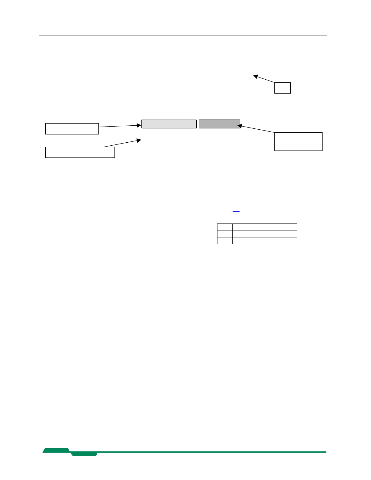
6.3 Profile processing
All camera settings are loaded or stored as complete data blocks (= Profiles). There are 17 profiles, the
Camera profile, the PowerUpProfile, eight factory profiles and eight user profiles.
user
profile 0
user
profile 1
user
profile n
user
profile 7
:p0
factory
profiles
0...7
f0..7
PowerUpProfile
:pc
:gc
or power on
:g7
camera profile (programs to camera logic)
configuration commands
:a..z[parameter]
:gn
:
g
1
:
g
0
:p1 :pn
:p7
6.3.1 Read Camera profile
The response to the read Camera profile command :w is a hex string of the contents of all actual camera
registers.
Command: :w
Response(e.g.): 6d774ac800006a1c6100851898c0003ff3ff
0000800300000000000000000000000000000000000000
all values hex, e.g.: 70
HEX
= 112
DEC
Sequence of transmitted data bytes:
A1 A2 A3 A4 A5 A6 A7 A8 Sa1 Sa2 Sa3 Sb1 Sb2 Sb3 R1h R1l ... R15h R15l ↵
A1...A8 image level control (FPN, contrast…)
Sa1 Sa2 Sa3 3 Byte synthesizer code of pixel clock
Sb1 Sb2 Sb3 3 synthesizer code of sensor clock
(see chapter
6.7.1 )
R1…R15 image control (image position, size, sync….)
R1h ... high Byte R1
R1l ... low Byte R1
↵ ... CR+LF (0dh + 0ah)
6.3.2 Write user profile
The PowerUpProfile is transferred to one of the eight user profiles.
Command: :p<n> <n> = 0 ... 7,c
L
Issue this command only, if the PowerUpProfile was
successfully tested.
15
Configuration MC13xx Users Manual Rev. 1.19
16
6.3.3 Load user profile
Load one of eight user profiles to the PowerUpProfile.
Command: :g<n> <n> = 0 ... 7, c
6.3.4 Load factory profile
The eight factory profiles can be read but not changed by the user.
Command: :f<n> <n> = 0 ... 7
6.4 Video data width, Base/ Full Camera Link®
MC13xx can output video data with 2 x 8-Bit or 2 x 10-Bit via the „Base Camera Link®“ interface, or 8
x 8-Bit or 10 x 8-Bit data via the „Full Camera Link®“ interface. Use register 7 Bits 7/5 to select..
Video data width :r7[7] :r7[5]
2 x 8 0 0
2 x 10 0 1
8 x 8 1 0
10 x 8 1 1
Table 6.4-1
The 10 x 8 - Bit data width lowers the clock speed for a given bandwidth, and needs a compatible frame
grabber. The assignment of the 10 taps to the Camera Link® ports is described in chapter:10*8-Bit As-
signment.
There are no predefined profiles for 10 x 8 Bits stored in the MC131x. Any predefined 8 x 8-Bit profile
can be used as starting point. Then change :r7 [7,5] to 1 and set Pixel Clock speed as described in:
Frequencies for video data width 10*8 - Bit. This profile can then be stored as User Profile.
*
MC130x: Setting of r7[7] is ignored by the camera.
MC131x: After a change of r7[7], change the selected
frequency. See: Table selection of clock frequencies.
6.5 Image quality
There are three D/A converter to influence image quality: FPN, Gain, and Black up. FPN, Gain and
especially Black might be adjusted if sensor clock changes. All three parameters are stored in nonvolatile memory as part of the selected profile.
6.5.1 FPN
The Fixed Pattern Noise setting reduces the fixed pattern noise that is typical to CMOS sensors. This
level might be changed if the sensor clock frequency is changed. For adjustment set the lens out of focus and to a medium grey level. Lower FPN until a heavy pattern appears. Then raise by a few points.
Command: :a1<x
1x0>
<x1x0> : Range, typ. 55h ... 80h
Response: none
Configuration MC13xx Users Manual Rev. 1.19
17
6.5.2 Gain
This is the threshold for the A/D converters. Its standard value is 66h for app. 1V. One step is app.
10mV. To increase the gain the value of a2 must be lowered.
Command: :a2<x1x0> <x1x0> : Range,
typ. 30h ... 80h
6.5.3 Black Level
Change Black Level if sensor clock changes. Increase this parameter until grey values in no light condition (closed lens) are close to zero.
Command: :a5<x1x0> <x1x0>: Range, typ. 00h ...ffh
Response: none
6.6 Image size and position
Image size and position within the sensor is defined by four parameters:
Bit(s) Description
r1[9..0] Number of first line, 0..3FD
h
r3[9..0] Number of lines, 0..3FF
h
r4[6..0] Address/10 of the first pixel
r5[6..0] Address/10 of the last pixel
Table 6.6-1
6.6.1 Address of the first line
Register r1 defines the first line to be displayed.
Command: :r1<x2x1x0>
<x
2x1x0
> ... Range 000h ...3fdh
Response: none
Example: :r1100
100h = image starts at line 257
L
If dual column binning is activated, r1 is doubled
within the camera logic.
6.6.2 Number of lines
Register r3 defines the number of lines to output.
Command: :r3<x2x1x0>
<x2x1x0> ... Range 000 h ...3ffh
Response: none
Example: :r3200 200h = display 513 lines
L
The sum of r1 and r3 must be ≤ 0x3ff/1023 or
0x1ff/511 if dual column binning is activated!

Configuration MC13xx Users Manual Rev. 1.19
18
6.6.3 Address of the first pixel of a line
Register r4 defines the leftmost pixel. The value is the pixel address divided by ten.
Command: :r4<x2x1x0>
<x2x1x0> ... Range 000h ...7fh
Response: none
Calculation of the value of r4:
Value of r4 = Pixel-Nr./10
6.6.4 Address of the last pixel of a line
Register r4 defines the rightmost pixel. The value is the pixeladress divided by ten.
Command: :r5<x2x1x0>
<x2x1x0> ... Range 000h ...07fh
Response: none
Calculation of the value of r5:
Value of r5 = Pixel-Nr./10
L
The difference r5 - r4 must be in the range: 0 ≤ r5-r4 ≤ 7fh .
6.6.5 Tracking
For rapid window movement even at slow baud rates a short command is provided..
command: :t<n>,<m>
<m> = X-position in pixel/10,
range 00h ...07fh
<n> = Y-position in lines / 4,
range 00h ...0ffh
Response: none
6.6.6 Arbitrary shaped fields of view
Standard adjustment of the camera using the parameters address of 1. pixel in a line, address of last
pixel in a line, address of first line and number of lines only allows to define one rectangular window .
For more than one window MC13xx offers a separate function, which allows to select more fields of
iew with different shapes.
It can be adjusted by a selection mask consisting of 16.384 read tiles. Each tile has a size of 10(H) x
8(V). All 16.384 tiles cover the whole active sensor area.
The selected tiles are summed up in 2.048 selection bytes with 8 bit and can be loaded sequentially via
register r8. Each set bit in a selection byte causes the associated tile to be captured and read out.

Configuration MC13xx Users Manual Rev. 1.19
19
The 1. of 2048 selection bytes addresses the leftmost, top pixel group with 10 pixel in the 1.-8. line (1.
selection tile). If bit 1 ist set the next 10 pixel of line no. 1-8 are activated. Bit7 enables pixel 70..79.
The next selection byte, bit0 addresses pixel 80..89.
command: :r8<x2x1x0>
<x2x1x0> ... range 000h ...03ffh
<x1x0> ... selection byte, bits 7..0, range 00h ...0ffh
<x2> ... , bit 9..8 = 0 : disable arbitrary window function
<x2> ... , bit 9..8 = 1 : write 2048 selection bytes
<x2> ... , Bit 9..8 = 2 : enable arbitrary window function,
disable write selection byte function
To set the arbitrary shaped field of view all 2048 selection bytes must be written. In each byte at least
write bit (bit8) must be set. After all 2048 selection bytes have been programmed the write function
must be finished by disabling the write function (2049. command).
The whole command list should be stored into a separate configuration file (*.mcf):
byte1 byte2 … byte n byte n+1… byte2048 byte2049
:r8100 :r8100 … :r81ff :r81ff … :r8100 :r8200
One command is only complete, if it starts with a colon, “r8” and then 2 ascii characters. To get a better
readability of the list it is recommended to start with a new line after 16 commands (CR+LF). The
single commands :r8200 and :r8000 will enable and disable the function.
The programmed settings of the 2048 bytes are volatile and must be programmed new after each power
up. The file may be written with the camera tool MC13xx using the function “Write” “File to camera”.

Configuration MC13xx Users Manual Rev. 1.19
20
6.7 Clock selection
The MC13xx is equipped with a 2-channel programmable clock synthesizer. One channel controls clock
frequency of the sensor (sensorclock, F
sens
), the other controls the frequency of the pixel clock (pixel-
clock, F
pix
). These independent clocks allow an always optimal ratio depending on the product of (im-
age size • image frequency) and the data rate on the output.
Example:
The MC13xx is connected to a frame grabber with a maximum data rate of 66MBytes/s via the„Base
Camera Link®“ interface using
2 x 8 bit video data.. A pixel clock of 33 MHz has to be selected.
As the sensor outputs 10 pixel per clock a sensor clock of 6.6MHz could be chosen. Because the sensor
can run up to a clock frequency of 66 MHz only 1/10 of the sensors possible speed would be used. To
make use of the maximum sensor clock and maintaining the maximum data rate on the output, just 120
(1280/10 rounded to steps of 10) from the possible 1280 pixel per line can be selected.
Therefore the ratio of F
sens
and F
pix
depends on the selected line length:
F
sens
<= (F
pix
• 1280) / (5 * line length)
or if 100 pixel line length is chosen:
F
sens
= (33 • 1280) / (5 • 100) = 70,4 MHz
As this exceeds the maximum sensor clock frequency, F
sens
is chosen as 66 MHz and F
pix
as 33 MHz.
6.7.1 Arbitrary selection of sensor and pixel clock
Sensor and pixel clock can be set to any value, the product of: (sensor clock • line length/1280) must
always be smaller (about 10%) than the qoutient: (pixel clock / video data width, e.g.: 2, or 8).
If
video data width of 10 x 8-Bit is selected, sensor clock = pixel clock.
command :S <x
0
>
<x
0
> ... 6 characters, as described in chapter Frequency selection
6.7.2 Table selection of clock frequencies
To simplify clock selection when using video data width of 2, clocks can be selected from a table with
15 entries, each entry being optimized for four regions of line length. (see table in 9.3).
Example: 240 < line length <= 640 Pixel, clock selection s9
pixelclock: 30,0 MHz
sensorclock: 11,2 MHz
resulting max. datarate on the 16-Bit output:
30,0 MHz/s * 2 Byte = 60,0 Mbyte/sec.

Configuration MC13xx Users Manual Rev. 1.19
This is valid for a line length between 250 and 640 pixel.
command :s <x0>
<x0> ... range 0 ... f (hex)
*
Before selecting the data rate of the camera check
the maximum data rate of the frame grabber, which
must be higher (or at least the same).
6.7.3 Image Format/Speed change
There are several steps necessary for a change of image format:
i. Disable sensor controller with :r6[4] = 0.
ii. Set image size with (:r1,:r2, :r3, :r4, :r5).
iii. If new sensor clock = old sensor clock:
1. Do not set pixel clock nor sensor clock.
iv. If new sensor clock > old sensor clock:
1. Set new pixel clock (:S6…..), then new sensor clock (:S4….).
v. If new sensor clock < old sensor clock:
1. Set new sensor clock (:S4…..), then new pixel clock (:S6….).
vi. Reenable sensor controller (:r6[4]=1).
6.8 Exposure control
Exposure control is selected with register r6[7..4] and register r2[9..0].
Bit(s) Description
r6[7..4] Type of exposure
r2[9..0] Exposure time
table 6-1
6.8.1 Type of exposure
The MC13xx can expose the images synchronous or asynchronous. An external signal on CC1 can be
used to synchronize MC13xx cameras to each other or to an external event.
6.8.1.1 Synchronous exposure
Synchronous exposure means that the next image is exposed, while the current image is output. This
mode provides fastest frame rate while maintaining maximum exposure time as long as 1/frame rate. If
an external synchronization signal is input on CC1 its frequency range can be between 30Hz and the
selected free running frame rate. Use MC13xx camera configuration tool for selection.
21

Configuration MC13xx Users Manual Rev. 1.19
22
6.8.1.2 Asynchronous exposure
With asynchronous exposure, an external signal starts exposure, and the exposed image is output immediately after the exposure ends. Exposure time is defined either by an internal timer or by the width of
the external EXP (CC1) signal. The time between two consecutive EXP (CC1) edges can be indefinite.
Frame rate = 1/(exposure time + image output time). Image output time equals the selected free running
frame rate. Use MC13xx camera configuration tool for selection.
The following registers select exposure type:
Register Bits :r6[7..4] :r7[8] :rf[0]
camera stop xxx0 x x
Synchronous without elec-
tronic shutter
0001 0 0
Synchronous with electronic
shutter
0011 0 0
Synchronous with electronic
shutter and external synchronisation signal, positive edge
0011 0 1
Synchronous with electronic
shutter and external synchronisation signal, negative edge
0011 1 1
Asynchronous, pulsewidth,
positive edge
1011 0 0
Asynchronous, pulsewidth,
negative edge
1011 1 0
Asynchronous, timer, positive
edge
1111 0 0
Asynchronous, timer, negative edge
1111 1 0
Table 6.8-1
6.8.2 Frame rate with synchronous exposure
The frame rate with synchronous exposure is direct proportional to the selected number of lines.
The time for one line is:
Tzz = 1/F
sens
• 136 [sec]
Tzz ...time/line
F
sens
... Sensorclock
Frame rate: = 1 / (time/line • number of lines+1) or:
= F
sens
/ (136 • (r3[9..0] +2))
Dependencies between image size and frame rate for typical clock frequencies are given in the following table:

Configuration MC13xx Users Manual Rev. 1.19
23
image size
100x100 240x240 640x480 1280x1024
Senso rclock (MHz) 66 33 13,2 6,6
Time/line [µs] 2,06 4,12 10,3 20,6
Frames/s 4.852 1.011 202 47
Table 6.8-2
6.8.3 Synchronous operation without shutter
Without electronic shutter the exposure time is 1 / frame rate.
6.8.4 Synchronous operation with shutter
In the sensor is implemented a freeze frame shutter, which allows to reduce the exposure time in steps
of one line. The minimum value of the exposure time is the duration of 2 line periods, which is determined by the value of r2 (min. 001h).
Command: :r2<x2x1x0>
<x2x1x0> ... Range 001h ...3ffh
Response: none
Exposure time TB :
TtB = r2 • TZZ -T
ZZ
/ 2
T
B
... exposure time in s B
r2 ... value of register 2
T
ZZ
... time/line
T
zz
= 1/F
sens
* 136 [s]
Ttzz ... Time/line
F
sens
... sensor clock
Typical exposure times:
Sensor clock
frequency (MHz)
Time/line
(µsec)
r2
@ 1/5.000 s
r2
@ 1/10.000 s
66 2,06 97 49
33 4,12 49 24
13,2 10,3 19 10
6,6 20,6 10 5
Table 6.8-3
6.8.5 External synchronisation with synchronous exposure
MC13xx cameras can be synchronized to an external signal that is input on the EXP (CC1) signal. The
strobe output signal of a MC13xx “master camera” can be used for that purpose. The attached frame
grabber must provide the connection of an external input to the CC1 signal to the camera. The frame
grabber is initialized for a MC13xx in free running mode.
See timing diagram: Synchronous exposure with external synchronisation via CC1
The cameras frame rate must be set to a frequency slightly higher than the maximum frequency of the
synchronization signal. The minimum frequency should be higher than 30Hz.

Configuration MC13xx Users Manual Rev. 1.19
24
Command: :rf<0|1>
<0> ... deselect external sync signal
<1> ... select external sync signal
Response: none
Make sure that a sync signal is present on EXP/CC1 before this command is issued or the “trigger on
CC1” button is pressed on the MC13xx camera configuration tool.
The polarity of the sync signal can be selected with the _Polarity_of_EXP-signal
6.8.6 Frame rate with asynchronous exposure
The frame rate with asynchronous exposure = Frame rate with synchronous exposure – (1 / exposure
time).
6.8.7 Asynchronous exposure, shutter control by pulse width
This operating mode is selected with register 6:
:r6[7..4] = 0xb
Exposure time depends on the width of the external EXP – signal.
6.8.8 Asynchronous exposure, shutter control by timer
This operating mode is selected with register 6:
:r6[7..4] = 0xf
The asynchronous exposure time is dependent on :r2[9..0]. The exposure timer counts as many lines as
are defined in register :r2[9..0].
Exposure time:
TB = 1/F
sens
* 136 • (1+r2[9..0]) [Sec]
T
B
... exposure time
F
sens
.. sensor clock
example: sensor clock = 66MHz
value of r2[9..0] = 6
T
B
= 136 • 6 • 15 ns = 12,2 µs

Configuration MC13xx Users Manual Rev. 1.19
25
6.9 Firmware
6.9.1 Update Firmware
MC13xx’s logic is integrated into a FPGA (Field Programmable Gate Array), which’s configuration is
stored in an EEPROM. Upon power up or a command the FPGA is loaded with this configuration. Configuration data can be downloaded via the serial interface of Camera Link®. Mikrotron may provide
configuration files (*.ibf) on request.
After download of configuration data, this data is permanently stored in EEPROM and the FPGA is
configured with the new data. Besides a power cycle, the :c command can be used to reconfigure the
FPGA with the internally stored configuration data.
*
Download of *.ibf file via serial link with 9600Bd takes app. 1.5-5
min depending on the used camera. There should be no loss of
power or communication during this time!
6.9.2 Reset and configuration of the internal FPGA
The command :c executes a reset in the camera. The FPGA will be reconfigured and all internal regis-
ters reloaded with the last saved PowerUpProfile. The FPGA is also configured after each power up.
Command: :c
Response: none
6.10 Horizontal pixelbinning
Pixelbinning adds the gray values of two adjacent pixels and outputs it as one pixel with double sensitivity. In X-direction only 512 pixels are needed to cover the sensors full size.
To retain aspect ratio, every second line is discarded, if this feature is not disabled by setting Bit 8 of
register 6 (:r61xx) or vertical pixelbinning is activated.
Command: :r7010
Response: none
If discarding of every other line is not disabled (:r61xx), the contents of :r1 is doubled in camera logic.
To address a specific line on the sensor, the value written into :r1 has to be divided by two and :r3 must
not exceed 1ffh.
Example:
To output 256 lines from line 128, set r1 = 63 and r3 = 255 (=0xff).
6.11 Vertical pixelbinning
Vertical pixelbinning adds the gray values of two superimposed pixel of a column. This doubles sensitivity and vertical field of view. To retain aspect ratio, in addition horizontal binning must be activated.
To activate, set bit 2 in register 6.
Command example: :r6034
Response: none

Configuration MC13xx Users Manual Rev. 1.19
26
6.12 Digital shading correction
For the best possible image quality even at the sensors clock limit, and non uniform lighting, the
MC13xx can store gray levels along one line and subtract these from all lines of an image.
To setup shading correction set: :r6[1] = 0.
Then a uniform object should be used together with the desired lighting, exposure mode and time and
lens. The lens should be closed so that the remaining light level along the center line of the image is as
close to zero as possible, but not reaching zero.
Then set :r6[1] = 1.
The gray levels along the center line of the image are saved in volatile memory and then subtracted
form all lines of the following images, as long as this bit remains set.
6.13 Digital gain
Digital gain selection is only possible with video data width 2 x 8-Bit or 8 x 8-Bit. Out of the 10-bits
sensor data either the most significant 8 bits (gain 1), or bits 8..1 (gain 2), or the least significant 8 bits
(gain 4) are selected.
Command: :r700x
x = 0: gain 1
x = 4: gain 2
x = 8: gain 4
6.14 External clock input
MC13xx frequency synthesizer can use the Camera Link® used to synchronize several MC13xx to one
master clock.
To activate set Bit 9 of register 7.
Command example: :r7200
response: none
*
If the external reference clock is different from
3.6864 MHz, the codes for the clock synthesizer have
to be recalculated.
6.15 Polarity of EXP-signal
The polarity of the EXP-signal can be positive- or negative active.
Use :r7[8] to select.
Negativ = :r7[8] = 1
Positiv = :r7[8] = 0
Command example: :r7100
Response: none

Configuration MC13xx Users Manual Rev. 1.19
27
6.16 Test image
For testing of camera logic and video data transmission, sensor data can be replaced by an internal gray
scale pattern with pixel values of 0..127. Use digital gain command to see pixel values of 0..255.
Command example: :r7040 r7[6]
Response: none
6.17 Image counter
If a sequence of frames is to be recorded for long time at a high frame rate, it can be useful to mark the
images for later identification or check for completeness.
MC13xx has a 16-Bit image counter whose count can replace the first two pixel of every image. The
image counter is cleared with every low to high transition of r7[1], the camera enable bit. It is incremented by every new image.
Command example: :r7002 r7[1]
Response: none
6.18 ImageBLITZ® shutter release, MC131x only
The ImageBLITZ® shutter release is only implemented in MC131x, not in MC130x.
ImageBLITZ can replace an external signal (e.g.: a light barrier) to release the shutter. Like a light barrier, ImageBLITZ is used to capture fast moving objects on the exact same position on the image.
Contrary to the light barrier, ImageBLITZ uses the same information as condition to release the shutter
as the then exposed image.
ImageBLITZ defines one specific line or a part of the 1024 lines as trigger window. This is true even if
the selected image size is less 1024 lines or outside of the selected image area.
After activation of ImageBLITZ and after issuing the EXP signal as an enable signal, the MC131x
hardware checks the gray values in the trigger window at a repetition rate that is defined by the exposure time selected with bits 3..0 of r6.
If a selectable number of pixels along that trigger window exceed or fall short of a selectable threshold,
one single image is exposed and output.
To adjust ImageBLITZ®, the trigger line can be superimposed to the image. Within the selected line, 10
pixel are displayed as a dotted black- and white line as long as the selected threshold is not passed.
ImageBLITZ is configured with the registers r8..rCh:

Configuration MC13xx Users Manual Rev. 1.19
6.18.1 ImageBLITZ® processing
When ImageBLITZ® is activated with :r7h[0] = 1:
1. Wait for an active edge on the EXP input.
2. The MC13xx exposes a line, that was chosen with :rC[9..0] and is called trigger line, for an
exposure time defined by :r2[9..0]. It compares the intensity of a group of 10 pixel along the
selected trigger line against an adjustable threshold (:rAh[7..0], Range: 255..0).
3. The number of exceedings (:rAh[8] = 0) or fall backs (:rAh[8] = 1), are counted, and the result is compared to a second threshold (:rBh[6..0], Range: 127..0).
4. Each time this threshold is exceeded (release condition); an “inhibit counter” (:rDh[9..0],
Range 1..255) is loaded.
5. The inhibit counter” :rDh[9..0] is counted down, each time the “release condition” was not
reached. Once this “inhibit counter” has expired, a new image is exposed and output.After
image is output, repeat at 1.
6.18.2 ImageBLITZ® programming
ImageBLITZ® is programmed by registers r8..rDh and activated with r7[0].
6.18.2.1 Address of trigger line
The register rCh determines the vertical position of the trigger line in the image.
command: :rCh <x2x1x0>
<x2x1x0> ... range 00h ...3ffh
Response: none
Example: :rc100
100h = 256
L
In pixelbinning mode the value of rC is internally
doubled. The value must not be higher than
1ffh/511.
6.18.2.2 Leftmost pixel of the trigger line
The value of register r8 / 10 is the number of the leftmost pixel in the trigger line.
Command: :r8<x2x1x0>
<x2x1x0> ... range 000h ...07fh
Response: none
Calculation of r8:
Value of r8 = pixel number / 10
28

Configuration MC13xx Users Manual Rev. 1.19
29
6.18.2.3 Rightmost pixel of the trigger line
The end of the trigger line is determined by the value of register r9.
Command: :r9<x2x1x0>
<x2x1x0> ... range 000h ...7fh
Response: none
Calculation of r9:
Value of r9 = pixel number / 10
6.18.2.4 Threshold level, mark trigger line
The threshold level is set by register rAh . The pixel values along the trigger line are compared with this
value.
Command: :rAh <x2x1x0>
<x1x0> ... range 0 ..ffh
<x2> = 0: pixel gray level > threshold level,
trigger line not visible
1: pixel gray level < threshold level,
trigger line not visible
2: pixel gray level > threshold level,
trigger line visible
3: pixel gray level < threshold level,
trigger line visible
Response: none
The trigger line is displayed as dashed, black and white line. One dash has a length of 10 pixel. The
trigger line is only displayed in parts of the line where the pixel fulfill the trigger requirements.
Under normal operation conditions the trigger line will be visible only in parts. The number of dashes
may be counted and used for the setting of register rBh.
6.18.2.5 Release condition
Register rB
h
contains the release condition.
The release condition is determined by the number of pixels along the triggerline that fulfill the trigger
requirements.
Command: :rB
h
<x
9..0
>
<x
6..0
> = 0 ..7fh, number of pixel that match the trigger requirements
<x
8..7
= 0: correction value 0 for the X - position of output window
<x
8..7
= 1: correction value 4 for the X - position of output window
<x
8..7
= 2: correction value 8 for the X - position of output window
<x
8..7
= 3: correction value 12 for the X - position of output window
Response: none

Configuration MC13xx Users Manual Rev. 1.19
30
6.18.2.6 Release Inhibit
The Release Inhibit function is defined with :rDh. It tells ImageBLITZ how often sequentially the “re-
lease condition” must not be met, before an image is output.
This feature allows to trigger an object only once on the dark- to bright edge of the scene. This avoids
retriggering, once the trigger condition was met and the object is still visible within the triggerline after
the image has been output.
Command: :rDh <x
7..0
>
<x
7..0
> = 0 ..ffh, number of fulfilled,
sequentially trigger conditions
Response: none
6.18.3 ImageBLITZ® registers
Register Bit Description
r7 0 = 1: activate ImageBLITZ®
r8 6..0 First pixel mod. 10
r9 6..0 Last pixel mod. 10
rA
h
7..0
8
9
Exposure threshold
1: bright object triggers
0: dark object triggers
1: make triggerline visible
rB
h
6..0
8..7
9
Number of exceedings or fall backs, release condition,
X – tracking correction
X – tracking enable.
rC
h
9..0 Address of triggerline
rD
h
7..0 exposure limitation, number of exposures without
exposure condition until an image is captured
Table 6.18-1
Registers r1..r7 are programmed according to image size and position and for
Asynchronous operation,
timer .
Register Bit Description
r1, r3..r5 Image size and position
r2
r6
9..0
7..4
Async operation, timer
0fh
Table 6.18-2

Configuration MC13xx Users Manual Rev. 1.19
31
6.18.4 ImageBLITZ® setup
The MC131x is configured for asynchronous operation with timer , registers r8, r9 and rCh are loaded
for the desired position of the trigger line. Register rBh is loaded with 0, register rAh with 201
h,
so that
the trigger line is visible.
L
If the image is zoomed down for display by an application program, every other line may be omitted and the
trigger line may then disappear.
ImageBLITZ® is enabled with Register r7 Bit1=1.
Now position the trigger line with the registers r8, r9 and rCh across the object that is used for the shutter release..
Clear Bit 8 in Register rAh if a bright objects releases the shutter, set rAh[8] if dark objects release the
shutter. While the trigger line is placed across the object, raise threshold with rA
h
[7..0] until as many
dashes from the trigger line disappear as are loaded in Register rB
h
[6..0]. This is called the release con-
dition.
If it is expected that the release condition is met more than once for a single object, load rBh [9..7] with
a number of exposed lines that will not met the release condition before exposing one image.
MC13xx configuration tool MC13xx Users Manual Rev. 1.19
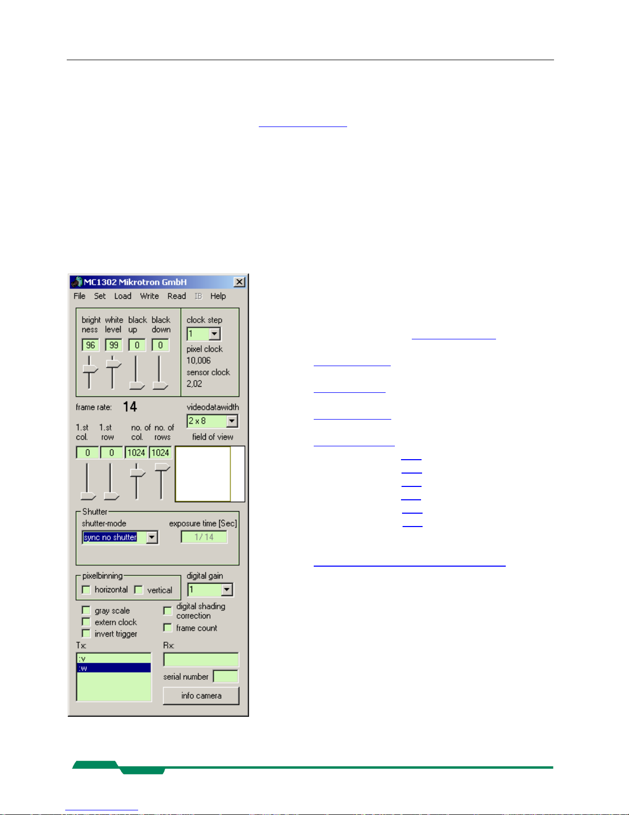
7 MC13xx configuration tool
The MC13xx configuration tool must be installed on a Windows PC. (Win9x, WinNT, Win2K, WinXP)
by means of the setup software. See also www.mikrotron.de to download the latest version.
This software provides an almost self explaining user interface to modify any camera parameter. The
description of the parameters follows the marked chapters in this user manual.
To use this tool with the camera MC13xx the serial interface is integrated in the Camera Link® interface. You do not need any other additional cable.
7.1 Basic Configuration
File: Save or read settings to or from file.
Set: Select com port. If Inspecta-4D and the cor-
rect cable is used, the MC13xx can be written to
but not being read from.
Load, Write, Read: Profile processing
FPN, Gain …:
Adjusting image
Clock Step:
Clock selection
1.st col…num. of rows:
Adjusting Image
Shutter:
Type of exposure
Frame count (6.17),
gray scale (6.16),
invert trigger (
6.15),
extern clock (
6.14),
digital gain (6.13)
pixelbinning……(6.10)
Info camera:
Read serial number and firmware version
Tx:
Display control strings
Rx:
Display response
32

MC13xx configuration tool MC13xx Users Manual Rev. 1.19
33
.2 ImageBLITZ® Configuration 7
1 Col, Num Of Col., Row ( Position of TriggerLine ):
r8, r9 and rC
ease Condition:
ease Inhibit:
e Visible:
Bit 8
ITZ Active:
Bit 0
bject Triggers:
Bit 9
st
Threshold:
rA
Rel
rB
Rel
rD
Lin
rA
ImageBL
r7
Bright O
rA

Mechanical dimensions MC13xx Users Manual Rev. 1.19
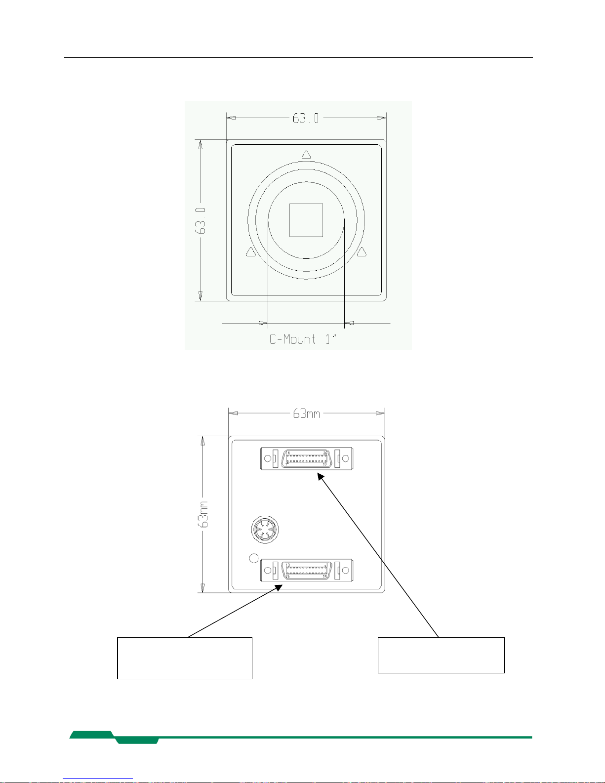
8 Mechanical dimensions
8.1 Camera body MC13xx
The camera body has (without lens) has very compact. To fasten the camera there are two mounting
holes M4x7mm and one tripod connection on each side available.
8.1.1 Dimensioned drawing, side view of MC1302/03/10/11
Cameralink® full
conf., MDR26connector, only with
MC1310/1311
8.1.2 Dimensioned drawing, side view of MC13x6 – MC13x9
75.4
70.0
48
31.5
63
58.6
M4 (8x)
W1/4"x7 (4x)
34
Mechanical dimensions MC13xx Users Manual Rev. 1.19
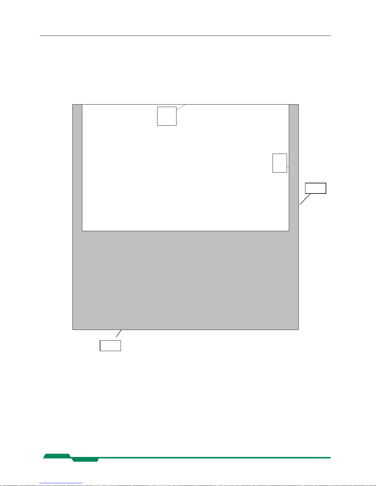
8.1.3 Dimensioned drawing, front view of MC1302/03/10/11
8.1.4 Dimensioned drawing, rear view of MC13xx
Cameralink® full conf.,
MDR26-connector
Cameralink® base conf.,
MDR26-connector
35

Mechanical dimensions MC13xx Users Manual Rev. 1.19
36
8.2 Lens adjustment
8.2.1 Lens adaption
In dependence of the camera model the MC13xx camera are prepared for either C-mount or F-mount
connection (see table overview of cameras).
Camera types with F-mount adaption may be converted to C-mount adaption by exchanging the lens
mount flange of the camera, which is attached with 4 screws. The C-mount lens flange is not scope of
delivery of the F-mount camera types and is offered separately.
8.2.2 Adjustable lens adapter, only for camera models with C-mount flange
For fine adjustment of the focal length a lens adapter with an adjustment range of ± 1 mm is provided.
Use the three screws nearby the sensor window to fasten the lens adapter after a proper adjustment together with the chosen lens.
8.2.3 Lens selection for camera types with C-mount flange (see table overview of cameras)
Due to the size of the sensor use C-Mount lenses with the largest possible optical diameter or an adapter
for lenses like F-Mount, especially for lenses with a focal length < 25mm..

Technical Data MC13xx Users Manual Rev. 1.19
37
9 Technical Data
MC1302 – MC1319 Monochrome
Bayer Filter
Number of pixel 1280 x 1024
Pixel size 12 x 12 µm
Active area 15,36 (H) x 12,29 (V) mm
Fill factor 40%
Sensitivity at 550 nm @ Vref
= 1V (a2 = 66h)
1600LSB/lux-sec
Spectral response 400..800nm
Shutter Electronic „Freeze Frame“ Shutter
Trigger Asynchronous shutter, shutter time
selectable with internal timer or by
pulse width of trigger signal
Internal Dynamic 59 dB
Power supply 8 ... 24 V
Power consumption max.
Thermal resistance typ.
3.5W
0.17°/W
Serial data link RS-644 with Camera Link®
9,6 – 115 KBd, 8 bits, 1 stop bit, no
parity
Digital video
MC131x
MC130x
Camera Link®, Base or Full con-
figuration
Camera Link®, Base configuration
Case temperature +5..50°C
Shock & vibration 70g, 7grms
Dimensions
(WxHxD)
63 x 63 x 47 mm
Case temperature +5 ... +50° C
Weight ca. 300 g
Lens mount C-/F-mount (depending on camera
type)
Table 8.2-1

Technical Data MC13xx Users Manual Rev. 1.19
9.1 Spectral response
38
Technical Data MC13xx Users Manual Rev. 1.19
9.2 Sensitive area of a pixel
Pixel size: 12 x 12 µm
Fill factor: 40 %
Sensitive area: 10,5 x 6,5 µm
Sensitive Area
6.5
µm
10.5
µm
12
µm
12
µm
39
Technical Data MC13xx Users Manual Rev. 1.19
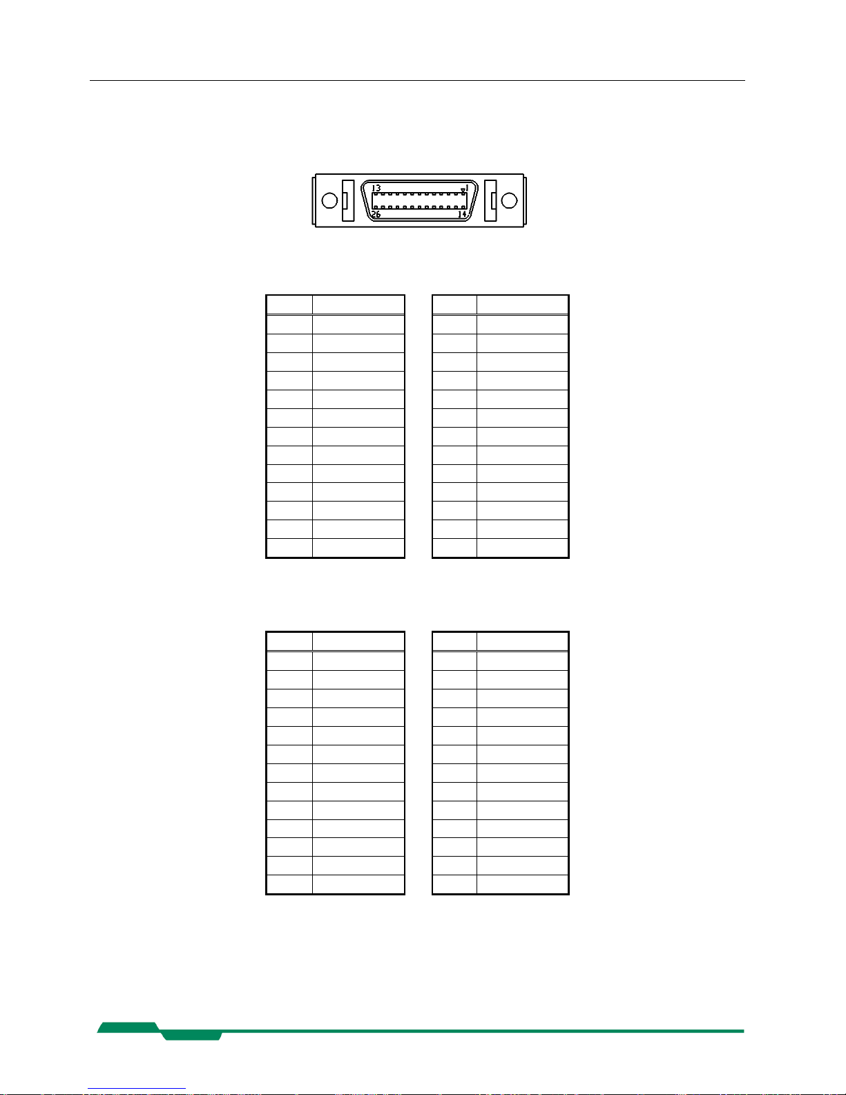
9.3 Connector pinning
9.3.1 Camera Link® Connector, MDR-26
„Base Camera Link® “ Pinning:
pin signal pin signal
1 GND 14 GND
2 X0- 15 X0+
3 X1- 16 X1+
4 X2- 17 X2+
5 XCLK- 18 XCLK+
6 X3- 19 X3+
7 SERTC+ 20 SERTC8 SERTFG- 21 SERTFG+
9 CC1- 22 CC1+
10 CC2+ 23 CC211 CC3- 24 CC3+
12 CC4+ 25 CC413 GND 26 GND
Table 9.3-1
„Full Camera Link® “ Pinning:
pin signal pin signal
1 GND 14 GND
2 Y0- 15 Y0+
3 Y1- 16 Y1+
4 Y2- 17 Y2+
5 YCLK- 18 YCLK+
6 Y3- 19 Y3+
7 100 Ω Term. 20 100 Ω Term
8 Z0- 21 Z0+
9 Z1- 22 Z1+
10 Z2- 23 Z2+
11 ZCLK- 24 ZCLK+
12 Z3- 25 Z3+
13 GND 26 GND
Table 9.3-2
manufacturer: 3M
Order-Nr. 10226-6212VC
40
Technical Data MC13xx Users Manual Rev. 1.19
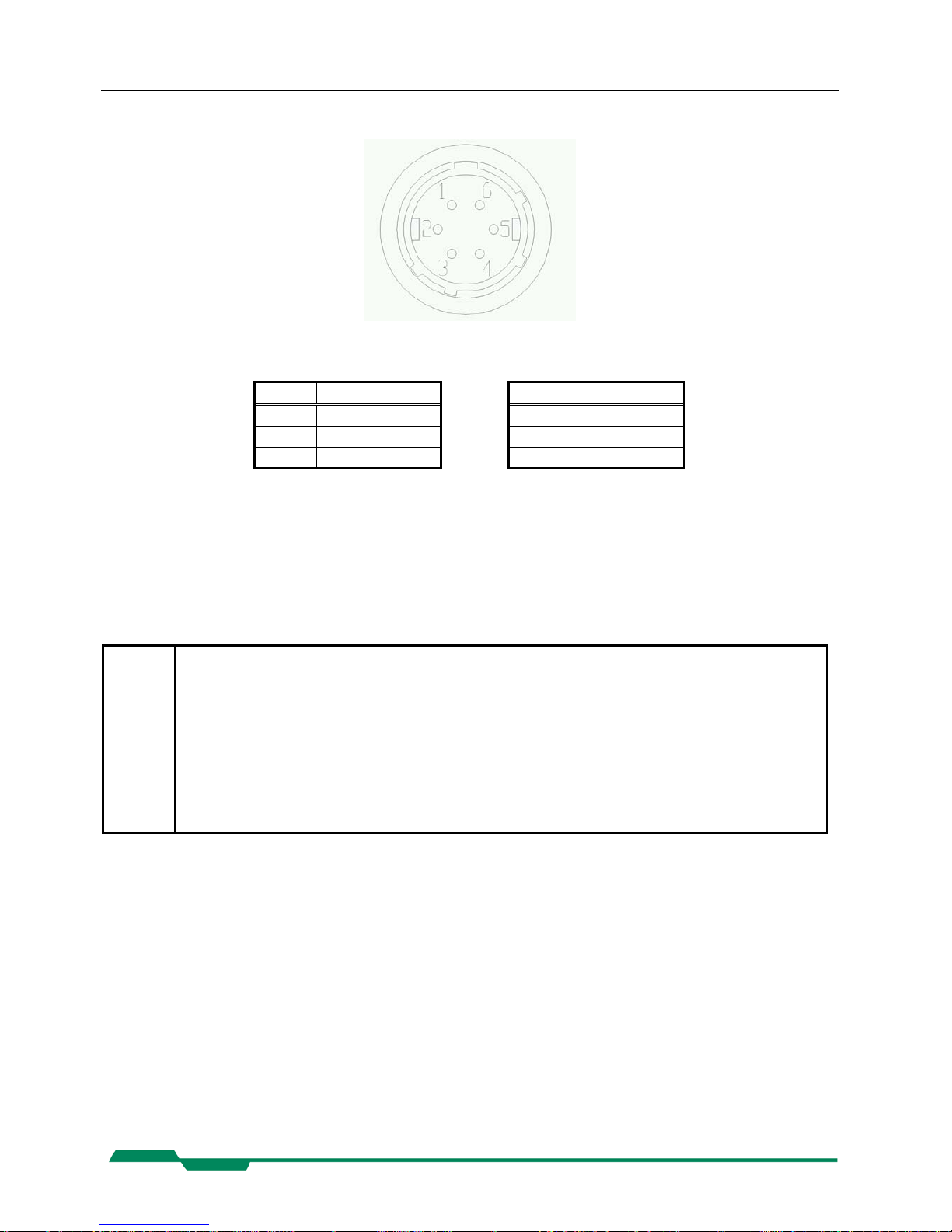
9.3.2 Circular power connector, 6-pin
pin signal pin signal
1 VCC 4 DGND*
2 VCC 5 GND
3 STRB 6 GND
Table 9.3-3
*DGND ... digital GND for signal STRB
Manufacturer: Hirose
Order no.: HR10A-7P-6S
*
Before applying power to the camera we strongly recommend to verify the used pins of the
power connector, the polarity (+/-) of the leads and the supply voltage.
The camera may only be used with a supply voltage according to the camera specification.
Connecting a lower or higher supply voltage, AC voltage, reversal polarity or using wrong
pins of the power connector may damage the camera. If doing so, the warranty will expire
immediately.
41

Technical Data MC13xx Users Manual Rev. 1.19
42
9.4 Camera Link® Bit Assignments
9.4.1 Base Camera Link® 2*8/10 - Bit Assignment
The following table shows the bit assignment of two adjacent pixel, eight or ten bits each. All unused bits are set to logical
LOW level, the SPARE outputs are set to logical HIGH level.
Plug 1, Camera Link X, 2*8-Bit Plug 1, Camera Link X, 2*10-Bit
Port Tx Signal Port Tx Signal
A0 0 D0 A0 0 D0
A1 1 D1 A1 1 D1
A2 2 D2 A2 2 D2
A3 3 D3 A3 3 D3
A4 4 D4 A4 4 D4
A5 6 D5 A5 6 D5
A6 27 D6 A6 27 D6
A7 5 D7 (msb) A7 5 D7
B0 7 D8 A8 7 D8
B1 8 D9 A9 8 D9 (msb)
B2 9 D10 LOW 9 LOW
B3 12 D11 LOW 12 LOW
B4 13 D12 B8 13 D18
B5 14 D13 B9 14 D19 (msb)
B6 10 D14 LOW 10 LOW
B7 11 D15 (msb) LOW 11 LOW
LOW 15 LOW B0 15 D10
LOW 18 LOW B1 18 D11
LOW 19 LOW B2 19 D12
LOW 20 LOW B3 20 D13
LOW 21 LOW B4 21 D14
LOW 22 LOW B5 22 D15
LOW 16 LOW B6 16 D16
LOW 17 LOW B7 17 D17
LVAL 24 LVAL LVAL 24 LVAL
FVAL 25 FVAL FVAL 25 FVAL
DVAL 26 DVAL DVAL 26 DVAL
SPARE 23 HIGH SPARE 23 HIGH
TxClk TxClk
Table 9.4-1

Technical Data MC13xx Users Manual Rev. 1.19
43
9.4.2 Full Camera Link® 8*8-Bit Assignment
The following table shows the bit assignment of eight adjacent pixel. All unused bits are set to logical LOW level, the
SPARE outputs are set to logical HIGH level.
Plug 1, Camera Link® X Plug 2, Camera Link® Y Plug 2, Camera Link® Z
Port Tx Signal Port Tx Signal Port Tx Signal
A0 0 D0 D0 0 D24 G0 0 D48
A1 1 D1 D1 1 D25 G1 1 D49
A2 2 D2 D2 2 D26 G2 2 D50
A3 3 D3 D3 3 D27 G3 3 D51
A4 4 D4 D4 4 D28 G4 4 D52
A5 6 D5 D5 6 D29 G5 6 D53
A6 27 D6 D6 27 D30 G6 27 D54
A7 5 D7 (msb) D7 5 D31 (msb) G7 5 D55 (msb)
B0 7 D8 E0 7 D32 H0 7 D56
B1 8 D9 E1 8 D33 H1 8 D57
B2 9 D10 E2 9 D34 H2 9 D58
B3 12 D11 E3 12 D35 H3 12 D59
B4 13 D12 E4 13 D36 H4 13 D60
B5 14 D13 E5 14 D37 H5 14 D61
B6 10 D14 E6 10 D38 H6 10 D62
B7 11 D15 (msb) E7 11 D39 (msb) H7 11 D63 (msb)
C0 15 D16 F0 15 D40 LOW 15 LOW
C1 18 D17 F1 18 D41 LOW 18 LOW
C2 19 D18 F2 19 D42 LOW 19 LOW
C3 20 D19 F3 20 D43 LOW 20 LOW
C4 21 D20 F4 21 D44 LOW 21 LOW
C5 22 D21 F5 22 D45 LOW 22 LOW
C6 16 D22 F6 16 D46 LOW 16 LOW
C7 17 D23 (msb) F7 17 D47 (msb) LOW 17 LOW
LVAL 24 LVAL LVAL 24 LVAL LVAL 24 LVAL
FVAL 25 FVAL FVAL 25 FVAL FVAL 25 FVAL
DVAL 26 DVAL DVAL 26 DVAL DVAL 26 DVAL
SPARE 23 HIGH SPARE 23 HIGH SPARE 23 HIGH
TxClk TxClk TxClk
Table 9.4-2

Technical Data MC13xx Users Manual Rev. 1.19
44
9.4.3 10*8-Bit Assignment
The below table shows the the assignment of 10 adjacent pixel, 8-Bit each. This assignment is compatible to Baslers A504 camera.
Plug 1, Camera Link® X Plug 2, Camera Link® Y Plug 2, Camera Link® Z
Port Tx Signal Port Tx Signal Port Tx Signal
A1 0 D0_0 D3 0 D3_2 G6 0 D6_5
A2 1 D0_1 D4 1 D3_3 G7 1 D6_6
A3 2 D0_2 D5 2 D3_4 G8 2 D6_7 (msb)
A4 3 D0_3 D6 3 D3_5 H1 3 D7_0
A5 4 D0_4 D7 4 D3_6 H2 4 D7_1
A6 5 D0_5 D8 5 D3_7 (msb) H3 5 D7_2
A7 6 D0_6 E1 6 D4_0 H4 6 D7_3
A8 7 D0_7 (msb) E2 7 D4_1 H5 7 D7_4
B1 8 D1_0 E3 8 D4_2 H6 8 D7_5
B2 9 D1_1 E4 9 D4_3 H7 9 D7_6
B3 10 D1_2 E5 10 D4_4 H8 10 D7_7 (msb)
B4 11 D1_3 E6 11 D4_5 I1 11 D8_0
B5 12 D1_4 E7 12 D4_6 I2 12 D8_1
B6 13 D1_5 E8 13 D4_7 (msb) I3 13 D8_2
B7 14 D1_6 F1 14 D5_0 I4 14 D8_3
B8 15 D1_7 (msb) F2 15 D5_1 I5 15 D8_4
C1 16 D2_0 F3 16 D5_2 I6 16 D8_5
C2 17 D2_1 F4 17 D5_3 I7 17 D8_6
C3 18 D2_2 F5 18 D5_4 I8 18 D8_7 (msb)
C4 19 D2_3 F6 19 D5_5 J1 19 D9_0
C5 20 D2_4 F7 20 D5_6 J2 20 D9_1
C6 21 D2_5 F8 21 D5_7 (msb) J3 21 D9_2
C7 22 D2_6 G1 22 D6_0 J4 22 D9_3
C8 23 D2_7 (msb) G2 23 D6_1 J5 23 D9_4
LVAL 24 LVAL G3 24 D6_2 J6 24 D9_5
FVAL 25 FVAL G4 25 D6_3 J7 25 D9_6
D1 26 D3_0 G5 26 D6_4 J8 26 D9_7 (msb)
D2 27 D3_1 LVAL 27 LVAL LVAL 27 LVAL
TxClk TxClk TxClk
Table 9.4-3

Technical Data MC13xx Users Manual Rev. 1.19
45
9.5 Frequency selection
Depending on the selected line length and the datarate on the “Camera Link®” interface the frequency
selection table can provide an optimal ratio of sensor /pixel clock. The pixel clock is only dependent on
the selected step and not on the linelength.
The sensor clock is dependent on both the selected step, the line length and the data width. The tables
show the selectable frequencies and the correponding codes to program the synthesizer accordingly.
9.5.1 Frequencies for video data width 2*8/10 - Bit, Base Camera Link®
9.5.1.1 Linelength <= 100 Pixel
clock
step
pixel clock
in MHz
Sensorclock
(MHz) for
linelength <= 100
Pixel
Framerate (fps) for
resolution: 100 x 100
Pixel
0 20,0 18,4 1352,9
1 20,0 24,5 1801,5
2 20,0 30,6 2250,0
3 20,0 36,9 2713,2
4 20,0 42,9 3154,4
5 21,8 49,0 3602,9
6 24,5 55,1 4051,5
7 27,2 61,2 4500,0
8 29,3 65,8 4838,2
9 30,0 67,4 4955,9
10 32,2 67,4 4955,9
11 35,3 67,4 4955,9
12 37,5 67,4 4955,9
13 42,9 67,4 4955,9
14 53,7 67,4 4955,9
15 63,3 67,4 4955,9
Table 9.5-1

Technical Data MC13xx Users Manual Rev. 1.19
46
9.5.1.2 Linelength <= 240 Pixel
Frequencies
Step
Pixelclock
(MHz)
Sensorclock
(MHz) for
linelength <=
240 Pixel
Framerate (fps) for
resolution: 240 x
240 Pixel
0 20,0 7,1 217,5
1 20,0 9,5 291,1
2 20,0 11,9 364,6
3 20,0 14,3 438,1
4 20,0 16,7 511,6
5 21,8 19,1 585,2
6 24,5 21,4 655,6
7 27,2 23,8 729,2
8 29,3 25,6 784,3
9 30,0 26,2 802,7
10 32,2 28,6 876,2
11 35,3 31,2 955,9
12 37,5 33,4 1023,3
13 42,9 38,1 1167,3
14 53,7 47,6 1458,3
15 63,3 57,1 1749,4
Table 9.5-2
9.5.1.3 Linelength <= 640 Pixel
Frequencies
Step
Pixelclock
(MHz)
Sensorclock
(MHz) for
linelength <=
640 Pixel
Framerate (fps) for
resolution: 640 x
480 Pixel
0 20,0 3,1 47,4
1 20,0 4,1 62,7
2 20,0 5,1 78,0
3 20,0 6,1 93,2
4 20,0 7,1 108,5
5 21,8 8,2 125,4
6 24,5 9,1 139,1
7 27,2 10,2 155,9
8 29,3 11,0 168,2
9 30,0 11,2 171,2
10 32,2 12,2 186,5
11 35,3 13,4 204,8
12 37,5 14,3 218,6
13 42,9 16,3 249,2
14 53,7 20,4 311,9
15 63,3 24,5 374,5
Table 9.5-3

Technical Data MC13xx Users Manual Rev. 1.19
47
9.5.1.4 Linelength <= 1280 Pixel
Frequencies
Step
Pixelclock
(MHz)
Sensorclock
(MHz) for
linelength <=
1280 Pixel
Framerate (fps) for
resolution: 1280 x
1024 Pixel
0 20,0 1,5 10,8
1 20,0 2,0 14,3
2 20,0 2,5 17,9
3 20,0 3,0 21,5
4 20,0 3,5 25,1
5 21,8 4,0 28,7
6 24,5 4,5 32,3
7 27,2 5,1 36,6
8 29,3 5,4 38,7
9 30,0 5,6 40,2
10 32,2 6,1 43,8
11 35,3 6,6 47,3
12 37,5 7,1 50,9
13 42,9 8,1 58,1
14 53,7 10,1 72,5
15 63,3 12,1 86,8
Table 9.5-4
Tolerance: ± 5 %

Technical Data MC13xx Users Manual Rev. 1.19
48
9.5.1.5 Respective codes for the clock synthesizer
Each frequency pair corresponds to two hexadecimal codes that are used to program the synthesizer.
These are also obtained on a read Camera Profile ( :w ) command.
Codes
Step
Pixel codes
in MHz
Sensor codes
(MHz) for:
10 < Linelength <= 100
Pixel
Sensor codes
(MHz) for:
100 < Line
length <=
240 Pixel
Sensor codes
(MHz) for:
240 < Line
length <=
640 Pixel
Sensor codes
(MHz) for:
640 < Line
length <=
1280 Pixel
0 612505 406d01 407182 416a85 416705
1 612505 416905 407181 40ee05 41be8b
2 612505 414088 41f988 41de09 407a81
3 612505 406c81 407102 416a05 416685
4 612505 41f489 41f10c 407182 405201
5 61fd09 416885 407101 40ed85 413207
6 616905 41f00f 416906 41f98b 410a05
7 61748b 414008 41f908 41dd89 407a01
8 61f08e 41e80c 41e890 41d188 40e203
9 61dc8d 40f405 40f487 411984 41da08
a 617489 -- 407082 416985 416605
b 610085 -- 407c82 40c105 41898c
c 61b489 -- 41f08c 407102 405181
d 61f489 -- 407081 40ed05 413187
e 60c005 -- 41f888 41dd09 41d589
f 617409 -- 407002 416905 416585
Table 9.5-5
There is a 3-byte code for each frequency. The code for the sensor clock is set to sb1…3 of a returned
PowerUpProfile (command :w).
The code of the pixel frequency corresponds to sa1…3.
Example: return of frequency codes
On command :w following answer was returned:
6d774ac800006a1c61788b41da080003ff3ff00007f030000000000000000000000000000↵
61dc8d... Sa1...3, pixel clock (see code of table 20 )
61dc8d = step 9, equivalent to 30,0 MHz
41da08... Sb1...3, sensor clock
according to table 20, mode 3
41da08= step9, equivalent to 5,6 MHz
07f.. Line length 1280 pixel

Technical Data MC13xx Users Manual Rev. 1.19
49
9.5.2 Frequencies for video data width 8*8 - Bit, Full Camera Link®
clock
step
pixel clock
in MHz
Pixelclock
program code
sensor clock
in MHz
Sensorclock
program code
Frame rate fps
0 20,0 :S612505 15,0 :S41dd0d 108
1 24,4 :S60c902 18,7 :S40e904 134
2 29,3 :S61f08e 22,5 :S40e903 161
3 34,6 :S612086 26,5 :S41c08e 188
4 39,1 :S60c883 30,0 :S41dc8d 215
5 43,9 :S61d088 33,7 :S41d08b 242
6 48,8 :S60c882 37,5 :S40e884 269
7 53,8 :S61e40f 41,2 :S41e089 296
8 58,5 :S61f00e 45,0 :S40e883 323
9 63,6 :S610806 48,7 :S40fc83 350
10 685 :S60f805 52,5 :S41d80f 376
11 70,9 :S61e80b 54,4 :S40e006 390
12 73,2 :S61f80b 56,2 :S40e806 403
13 75,8 :S611405 58,2 :S411007 417
14 78,2 :S60c803 60,0 :S41dc0d 430
15 81,1 :S607801 62,3 :S412407 447
Table 9.5-6
9.5.3 Frequencies for video data width 10*8 – Bit
Use the arbitrary frequency selection command:
command :S <x0>
<x0> 6 characters, programcode in the following table
clock
step
pixel clock
in MHz
Pixelclock
program code
sensor clock
in MHz
Sensorclock
program code
Frame rate fps
0 20,0 :S612505 15,0 :S41dd0d 108
1 24,4 :S60c902 18,7 :S40e904 134
2 29,3 :S61f08e 22,5 :S40e903 161
3 34,6 :S612086 26,2 :S41d88f 188
4 39,1 :S60c883 30,0 :S41dc8d 215
5 43,9 :S61d088 33,7 :S41d08b 242
6 48,8 :S60c882 37,5 :S40e884 269
7 53,8 :S61e40f 41,2 :S41e089 296
8 58,5 :S61f00e 45,0 :S40e883 323
9 63,6 :S610806 48,7 :S40d087 350
10 68,6 :S60f805 52,5 :S41d80f 376
11 70,9 :S61e80b 54,4 :S40e006 390
12 73,2 :S61f80b 56,2 :S40e806 403
13 75,8 :S611405 58,2 :S405411 417
14 78,2 :S60c803 60,0 :S41dc0d 430
15 81,1 :S607801 62,3 :S412407 447
Table 9.5-7

Technical Data MC13xx Users Manual Rev. 1.19
50
9.6 Programming sequence, factory profile f3
Example: resolution: 1.280 x 1.024 pixel
frame rate: 48 fps
pixel clock: 35,3 MHz sensor clock: 6,65 MHz
shutter: full frame , exposure time: 21 ms
Strings: :a16d
:a277
:a34a
:a4c8
:a5xx xx... may be any value 00h ... ffh
:a600
:a76a
:a81c
:r6000
:r1000
:r23ff
:r33ff
:r4000
:r507f
:r7000
:r6030
:r8000
:r9000
:ra000
:rb000
:rc000
:rd000
:re000
:rf000
:sb

Technical Data MC13xx Users Manual Rev. 1.19
9.7 Timing
9.7.1 Pixel clock
FVAL
LVAL
Data
tdh = 4.5 ±1 ns
Pixel clock
Tclk, 12..~200ns
The above illustration shows hold time of video data, LVAL and FVAL signal to rising edge of pixel
clock.
9.7.2 Line Valid (LVAL, DVAL)
LVAL,
DVAL
Tldvh
Tldvl
LVAL and DVAL are connected internally in the camera. The timing for the LVAL / DVAL signal
shown in multiples of the pixel clock depend on the ratio of sensor/pixel clock, on selected line length,
and on video data width. Tldvh is always the same for a specific setting of the above parameters, Tldvl
my vary by one clock from line to line. The LVAL / DVAL signal is also output while FVAL is
inactive.
51
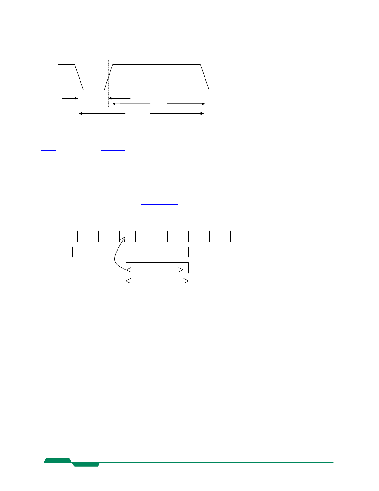
Technical Data MC13xx Users Manual Rev. 1.19
9.7.3 Frame Valid (FVAL)
52
The rising edge of FVAL marks that line, that is programmed in Register r1.
FVAL
tfdv
tfdvl
tfdvh
Tfdvh is equal to the value programmed in Register r3 multiplied with time/line. Tfdvl in synchronous
mode is equal to one time/line.
9.7.4 Exposure Signal EXP, to be input on CC1
The EXP signal (Camera Link™ CC1 signal) is positive active if register 7, Bit 8 = 0, negativ active if
register 7, Bit 8 = 1. EXP Signal may not be asserted while the previous image is output (FDV active)
The sensors exposure starts and the strobe output activates (texp, (1) three sensor clocks after the active
edge of the EXP signal (tshut), and ends up to 135 sensor clocks after deactivation (2).
1)
LDV
2)
image n-1 image n
exp. image n
texp
FDV
EXP
1) The active edge of the EXP signal clears the horizontal counter.
2) End of exposure time is synchronised with the internal
horizontal counter.
EXP is also used as enable signal for ImageBLITZ shutter release.

Technical Data MC13xx Users Manual Rev. 1.19
9.7.5 Synchronous exposure with external synchronisation via CC1
t
exp(n
)
Image
(n-1)
t
exp(n+1
)
Image
(n)
t
sync
LVAL
FVAL
STROBE
CC1
t
53
exp
: Exposure time selectable with register :r2
t
sync
: The synchronisation frequency must be smaller than the framerate to which the MC13xx is set and
greater 30Hz.
 Loading...