

Page 1

AT24CM02
I2C-Compatible (2-wire) Serial EEPROM
2-Mbit (262,144 x 8)
DATASHEET
Features
Low Voltage and Standard Voltage Operation Available
1.7V (VCC = 1.7V to 5.5V)
2.5V (V
Internally Organized 262,144 x 8 (2-Mbit, 256-Kbyte)
2
I
C-Compatible (2-wire) Serial Interface
100kHz Standard Mode, 1.7V to 5.5V
400kHz Fast Mode, 1.7 to 5.5V
1MHz Fast Mode Plus (FM+) 2.5V to 5.5V
Schmitt Trigger, Filtered Inputs for Noise Suppression
Bidirectional Data Transfer Protocol
Write Protect Pin for Full Array Hardware Data Protection
256-byte Page Write Mode
Byte Write and Partial Page Writes Allowed
Self-timed Write Cycle
All Write operations complete within 10ms max
Random and Sequential Read Modes
Built in Error Detection and Correction
High Reliability
Endurance: 1,000,000 write cycles
Data retention: 100 years
Green Package Options (Lead-free/Halide-free/RoHS Compliant)
8-lead JEDEC SOIC and Thin or Standard Thickness 8-ball WLCSP
Die Sale Options: Wafer Form and Tape and Reel Available
= 2.5V to 5.5V)
CC
Description
The Atmel® AT24CM02 provides 2,097,152 bits of Serial Electrically Erasable and
Programmable Read-Only Memory (EEPROM) organized as 262,144 words of
8 bits each. The device’s cascadable feature allows up to two devices to share a
common 2-wire bus. The device is optimized for use in many industrial and
commercial applications where low power and low voltage operation are
essential. The device is available in space-saving 8-lead JEDEC SOIC and 8-ball
WLCSP packages. In addition, the entire family is available in 1.7V (1.7V to 5.5V)
and 2.5V (2.5V to 5.5V) versions.
Atmel-8828E-SEEPROM-AT24CM02-Datasheet_012017
Page 2

Table of Contents
1. Pin Descriptions and Pinouts . . . . . . . . . . . . . . . . . . . . . . . . . . . . . . . . . . . . . . . . . . . . . . . . . . . . . 3
2. Device Block Diagram and System Configuration . . . . . . . . . . . . . . . . . . . . . . . . . . . . . . . . 4
3. Device Operation and Communication . . . . . . . . . . . . . . . . . . . . . . . . . . . . . . . . . . . . . . . . . . . . 5
3.1 Clock and Data Transition Requirements . . . . . . . . . . . . . . . . . . . . . . . . . . . . . . . . . . . . . . . . . . . . . . 5
3.2 Start and Stop Conditions . . . . . . . . . . . . . . . . . . . . . . . . . . . . . . . . . . . . . . . . . . . . . . . . . . . . . . . . . . 5
3.2.1 Start Condition . . . . . . . . . . . . . . . . . . . . . . . . . . . . . . . . . . . . . . . . . . . . . . . . . . . . . . . . . . . 5
3.2.2 Stop Condition . . . . . . . . . . . . . . . . . . . . . . . . . . . . . . . . . . . . . . . . . . . . . . . . . . . . . . . . . . . 5
3.3 Acknowledge and No-Acknowledge . . . . . . . . . . . . . . . . . . . . . . . . . . . . . . . . . . . . . . . . . . . . . . . . . . 6
3.4 Standby Mode . . . . . . . . . . . . . . . . . . . . . . . . . . . . . . . . . . . . . . . . . . . . . . . . . . . . . . . . . . . . . . . . . . . 6
3.5 Software Reset . . . . . . . . . . . . . . . . . . . . . . . . . . . . . . . . . . . . . . . . . . . . . . . . . . . . . . . . . . . . . . . . . . 7
4. Memory Organization . . . . . . . . . . . . . . . . . . . . . . . . . . . . . . . . . . . . . . . . . . . . . . . . . . . . . . . . . . . . . 8
4.1 Device Addressing . . . . . . . . . . . . . . . . . . . . . . . . . . . . . . . . . . . . . . . . . . . . . . . . . . . . . . . . . . . . . . . 8
5. Write Operations . . . . . . . . . . . . . . . . . . . . . . . . . . . . . . . . . . . . . . . . . . . . . . . . . . . . . . . . . . . . . . . . . . 9
5.1 Byte Write . . . . . . . . . . . . . . . . . . . . . . . . . . . . . . . . . . . . . . . . . . . . . . . . . . . . . . . . . . . . . . . . . . . . . . 9
5.2 Page Write . . . . . . . . . . . . . . . . . . . . . . . . . . . . . . . . . . . . . . . . . . . . . . . . . . . . . . . . . . . . . . . . . . . . . 9
5.3 Internal Writing Methodology . . . . . . . . . . . . . . . . . . . . . . . . . . . . . . . . . . . . . . . . . . . . . . . . . . . . . . 10
5.4 Acknowledge Polling . . . . . . . . . . . . . . . . . . . . . . . . . . . . . . . . . . . . . . . . . . . . . . . . . . . . . . . . . . . . . 10
5.5 Write Cycle Timing . . . . . . . . . . . . . . . . . . . . . . . . . . . . . . . . . . . . . . . . . . . . . . . . . . . . . . . . . . . . . . 11
5.6 Write Protection. . . . . . . . . . . . . . . . . . . . . . . . . . . . . . . . . . . . . . . . . . . . . . . . . . . . . . . . . . . . . . . . . 11
6. Read Operations . . . . . . . . . . . . . . . . . . . . . . . . . . . . . . . . . . . . . . . . . . . . . . . . . . . . . . . . . . . . . . . . . 12
6.1 Current Address Read . . . . . . . . . . . . . . . . . . . . . . . . . . . . . . . . . . . . . . . . . . . . . . . . . . . . . . . . . . . 12
6.2 Random Read . . . . . . . . . . . . . . . . . . . . . . . . . . . . . . . . . . . . . . . . . . . . . . . . . . . . . . . . . . . . . . . . . . 12
6.3 Sequential Read . . . . . . . . . . . . . . . . . . . . . . . . . . . . . . . . . . . . . . . . . . . . . . . . . . . . . . . . . . . . . . . . 13
7. Device Default Condition from Atmel . . . . . . . . . . . . . . . . . . . . . . . . . . . . . . . . . . . . . . . . . . . . 13
8. Electrical Specifications . . . . . . . . . . . . . . . . . . . . . . . . . . . . . . . . . . . . . . . . . . . . . . . . . . . . . . . . . 14
8.1 Absolute Maximum Ratings . . . . . . . . . . . . . . . . . . . . . . . . . . . . . . . . . . . . . . . . . . . . . . . . . . . . . . . 14
8.2 DC and AC Operating Range . . . . . . . . . . . . . . . . . . . . . . . . . . . . . . . . . . . . . . . . . . . . . . . . . . . . . . 14
8.3 DC Characteristics . . . . . . . . . . . . . . . . . . . . . . . . . . . . . . . . . . . . . . . . . . . . . . . . . . . . . . . . . . . . . . 14
8.4 AC Characteristics . . . . . . . . . . . . . . . . . . . . . . . . . . . . . . . . . . . . . . . . . . . . . . . . . . . . . . . . . . . . . . 15
8.5 Power-Up Requirements and Reset Behavior . . . . . . . . . . . . . . . . . . . . . . . . . . . . . . . . . . . . . . . . . 16
8.5.1 Device Reset . . . . . . . . . . . . . . . . . . . . . . . . . . . . . . . . . . . . . . . . . . . . . . . . . . . . . . . . . . . 16
8.6 Pin Capacitance . . . . . . . . . . . . . . . . . . . . . . . . . . . . . . . . . . . . . . . . . . . . . . . . . . . . . . . . . . . . . . . . 16
8.7 EEPROM Cell Performance Characteristics . . . . . . . . . . . . . . . . . . . . . . . . . . . . . . . . . . . . . . . . . . . 16
9. Ordering Code Detail . . . . . . . . . . . . . . . . . . . . . . . . . . . . . . . . . . . . . . . . . . . . . . . . . . . . . . . . . . . . 17
10. Ordering Code Information . . . . . . . . . . . . . . . . . . . . . . . . . . . . . . . . . . . . . . . . . . . . . . . . . . . . . . 18
11. Part Markings . . . . . . . . . . . . . . . . . . . . . . . . . . . . . . . . . . . . . . . . . . . . . . . . . . . . . . . . . . . . . . . . . . . . 19
12. Packaging Information . . . . . . . . . . . . . . . . . . . . . . . . . . . . . . . . . . . . . . . . . . . . . . . . . . . . . . . . . . . 20
12.1 8S1 — 8-lead JEDEC SOIC . . . . . . . . . . . . . . . . . . . . . . . . . . . . . . . . . . . . . . . . . . . . . . . . . . . . . . . 20
12.2 8U-11 — 8-ball WLCSP . . . . . . . . . . . . . . . . . . . . . . . . . . . . . . . . . . . . . . . . . . . . . . . . . . . . . . . . . . 21
12.3 8U-18 — 8-ball WLCSP . . . . . . . . . . . . . . . . . . . . . . . . . . . . . . . . . . . . . . . . . . . . . . . . . . . . . . . . . . 22
13. Revision History . . . . . . . . . . . . . . . . . . . . . . . . . . . . . . . . . . . . . . . . . . . . . . . . . . . . . . . . . . . . . . . . . 23
2
AT24CM02 [DATASHEET]
Atmel-8828E-SEEPROM-AT24CM02-Datasheet_012017
Page 3

1. Pin Descriptions and Pinouts
Table 1-1. Pin Descriptions
Pin
Number
1, 2 NC
3 A
4 GND
5 SDA
6 SCL
Pin
Symbol
2
Pin Name and Functional Description
No Connect: The NC pin is not bonded to a die pad. This pin can be
connected to GND or left floating.
Device Address Inputs: The A2 pin is used to select the device address
and corresponds to the fifth bit of the I
pin can be directly connected to V
2
C seven bit slave address. This
or GND, allowing up to two devices
CC
on the same bus for a total of 4-Mbit of EEPROM.
Refer to Note 1 for behavior of the pin when not connected.
Ground: The ground reference for the power supply. GND should be
connected to the system ground.
Serial Data: The SDA pin is an open-drain bidirectional input/output pin
used to serially transfer data to and from the device.
The SDA pin must be pulled-high using an external pull-up resistor (not to
exceed 10K in value) and may be wire-ORed with any number of other
open-drain or open-collector pins from other devices on the same bus.
Serial Clock: The SCL pin is used to provide a clock to the device and is
used to control the flow of data to and from the device. Command and
input data present on the SDA pin is always latched in on the rising edge
of SCL, while output data on the SDA pin is always clocked out on the
falling edge of SCL.
The SCL pin must either be forced high when the serial bus is idle or
pulled-high using an external pull-up resistor.
Asserted
State
— —
— Input
— Power
—
— Input
Pin
Type
Input/
Output
Write Protect: Connecting the WP pin to GND will ensure normal write
7 WP
operations. When WP is connected to V
memory are inhibited.
Refer to Note 1 for behavior of the pin when not connected.
Device Power Supply: The VCC pin is used to supply the source voltage
8 V
CC
to the device. Operations at invalid V
results and should not be attempted.
Note: 1. If either the A
wide variety of application environments, the pull-down mechanism is intentionally designed to be somewhat
strong. Once these pins are biased above the CMOS input buffer’s trip point (~0.5 x V
mechanism disengages. In any case, Atmel recommends connecting these pins to a known state whenever
possible.
all write operations to the
CC
voltages may produce spurious
CC
pin or the WP pin are not driven, they are internally pulled down to GND. In order to operate in a
2
NC
NC
A
GND
8-lead SOIC
1
2
3
2
4
Top View
8
V
CC
7
WP
6
SCL
5
SDA
8-ball WLCSP
Thin or Standard Thickness
V
CC
WP
SCL
SDA
8
7
6
Top View
NC
1
NC
2
A
2
3
GND
45
High Input
— Power
), the pull-down
CC
* Note: Drawings are not to scale
AT24CM02 [DATASHEET]
Atmel-8828E-SEEPROM-AT24CM02-Datasheet_012017
3
Page 4

2. Device Block Diagram and System Configuration
Figure 2-1. Block Diagram
A
GND
Hardware
Address
Comparator
Memory
System Control
Power
On Reset
Generator
V
CC
Module
High Voltage
Generation Circuit
Write
Protection
WP
Control
EEPROM Array
Row Decoder
1 page
Column Decoder
2
Data Register
Data & ACK
D
Input/Output Control
OUT
D
IN
Address Register
and Counter
SCL
Start
Stop
Detector
SDA
Figure 2-2. System Configuration Using 2-Wire Serial EEPROMs
V
CC
R
PUP(max) =
V
CC
SCL
SDA
WP
R
PUP(min) =
t
R(max)
0.8473 x C
VCC - V
I
OL
L
OL(max)
I2C Bus Master:
Microcontroller
GND
4
AT24CM02 [DATASHEET]
Atmel-8828E-SEEPROM-AT24CM02-Datasheet_012017
NC
NC
A
2
GND
Slave 0
AT24Cxxx
V
CC
WP
SDA
SCL
NC
NC
A
2
GND
Slave 1
AT24Cxxx
V
WP
SDA
SCL
CC
Page 5

3. Device Operation and Communication
The AT24CM02 operates as a slave device and utilizes a simple I2C-compatible 2-wire digital serial interface to
communicate with a host controller, commonly referred to as the bus Master. The Master initiates and controls
all Read and Write operations to the slave devices on the serial bus, and both the Master and the slave devices
can transmit and receive data on the bus.
The serial interface is comprised of just two signal lines: Serial Clock (SCL) and Serial Data (SDA). The SCL pin
is used to receive the clock signal from the Master, while the bidirectional SDA pin is used to receive command
and data information from the Master as well as to send data back to the Master. Data is always latched into the
AT24CM02 on the rising edge of SCL and always output from the device on the falling edge of SCL. Both the
SCL and SDA pin incorporate integrated spike suppression filters and Schmitt Triggers to minimize the effects
of input spikes and bus noise.
All command and data information is transferred with the Most-Significant Bit (MSB) first. During bus
communication, one data bit is transmitted every clock cycle, and after eight bits (one byte) of data have been
transferred, the receiving device must respond with either an acknowledge (ACK) or a no-acknowledge (NACK)
response bit during a ninth clock cycle (ACK/NACK clock cycle) generated by the Master. Therefore, nine clock
cycles are required for every one byte of data transferred. There are no unused clock cycles during any Read or
Write operation, so there must not be any interruptions or breaks in the data stream during each data byte
transfer and ACK or NACK clock cycle.
During data transfers, data on the SDA pin must only change while SCL is low, and the data must remain stable
while SCL is high. If data on the SDA pin changes while SCL is high, then either a Start or a Stop condition will
occur. Start and Stop conditions are used to initiate and end all serial bus communication between the Master
and the slave devices. The number of data bytes transferred between a Start and a Stop condition is not limited
and is determined by the Master. In order for the serial bus to be idle, both the SCL and SDA pins must be in the
logic high state at the same time.
3.1 Clock and Data Transition Requirements
The SDA pin is an open drain terminal and therefore must be pulled high with an external pull-up resistor. Data
on the SDA pin may change only during SCL low time periods. The SCL pin must be forced high when the serial
bus is idle, therefore an external pull-up resistor is recommended. Data changes during SCL high periods will
indicate a Start or Stop condition as defined below.
3.2 Start and Stop Conditions
3.2.1 Start Condition
A Start condition occurs when there is a high-to-low transition on the SDA pin while the SCL pin is stable in the
Logic 1 state. The Master uses a Start condition to initiate any data transfer sequence, therefore the Start
condition must precede any command. The AT24CM02 will continuously monitor the SDA and SCL pins for a
Start condition but the device will not respond unless one is given. Please refer to Figure 3-1 for more details.
3.2.2 Stop Condition
A Stop condition occurs when there is a low-to-high transition on the SDA pin while the SCL pin is stable in the
Logic 1 state. The Master uses the Stop condition to end a data transfer sequence to the AT24CM02 which will
subsequently return to the idle state. The Master can also utilize a repeated Start condition instead of a Stop
condition to end the current data transfer if the Master will perform another operation. Please refer to Figure 3-1
for more details.
AT24CM02 [DATASHEET]
Atmel-8828E-SEEPROM-AT24CM02-Datasheet_012017
5
Page 6

3.3 Acknowledge and No-Acknowledge
After every byte of data is received, the receiving device must confirm to the Master that it has successfully
received the data byte by responding with what is known as an acknowledge (ACK). An ACK is accomplished
by the transmitting device first releasing the SDA line at the falling edge of the eighth clock cycle followed by the
receiving device responding with a Logic 0 during the entire high period of ninth clock cycle.
When the AT24CM02 is transmitting data to the Master, the Master can indicate that it is done receiving data
and wants to end the operation by sending a Logic 1 response to the AT24CM02 instead of an ACK response
during the ninth clock cycle. This is known as a no-acknowledge (NACK) and when the Master sends this
Logic 1 during the ninth clock cycle, the AT24CM02 will release the SDA line so that the Master can then
generate a Stop or Start condition.
The transmitting device, which can be the bus Master or the Serial EEPROM, must release the SDA line at the
falling edge of the eighth clock cycle to allow the receiving device to pull the SDA line low to ACK the previous
8-bit word. The receiving device must release the SDA line at the end of the ninth clock cycle to allow the
transmitter to continue sending new data. A timing diagram has been provided in Figure 3-1 to better illustrate
these requirements.
Figure 3-1. Start Condition, Data Transitions, Stop Condition and Acknowledge
SDA
Must Be
Stable
SDA
Must Be
Stable
Acknowledge Window
SCL
SDA
Start
Condition
SDA
Change
Allowed
The relationship of the AC timing parameters with respect to SCL and SDA for the AT24CM02 are show in
Figure 8-1 timing waveform on page 15. The AC timing characteristics and specifications are outlined in
Section 8.4 “AC Characteristics” on page 15.
3.4 Standby Mode
The AT24CM02 features a low power standby mode which is enabled when:
A valid power-up sequence is performed (see Section 8.5).
A Stop condition received by the device unless it initiates an internal write cycle (see Section 5.).
At the completion of an internal write cycle (see Section 5.).
An unsuccessful match of the device type identifier or hardware address in the Device Address byte (see
Section 4.1).
The bus Master does not ACK the receipt of data read out from the device; instead it sends a NACK
response (see Section 6.).
12 89
Stop
Condition
Acknowledge
Valid
SDA
Change
Allowed
The transmitting device (Master or Slave)
must release the SDA line at this point to allow
the receiving device (Master or Slave) to drive the
SDA line low to ACK the previous 8-bit word.
The receiver (Master or Slave)
must release the SDA line at
this point to allow the transmitter
to continue sending new data.
6
AT24CM02 [DATASHEET]
Atmel-8828E-SEEPROM-AT24CM02-Datasheet_012017
Page 7

3.5 Software Reset
After an interruption in protocol, power loss, or system reset, any 2-wire part can be protocol reset by following
these steps:
1. Create a Start condition (if possible).
2. Clock nine cycles.
3. Create another Start condition followed by a Stop condition as seen in Figure 3-2.
The device should be ready for the next communication after above steps have been completed. In the event
that the device is still non-responsive or remains active on the SDA bus, a power cycle must be used to reset
the device (see Section 8.5.1 “Device Reset” ).
Figure 3-2. Software Reset
Dummy Clock Cycles
SCL
SDA
Start
Condition
8321
9
Start
Condition
Stop
Condition
AT24CM02 [DATASHEET]
Atmel-8828E-SEEPROM-AT24CM02-Datasheet_012017
7
Page 8

4. Memory Organization
The AT24CM02 is internally organized as 1,024 pages of 256 bytes each.
4.1 Device Addressing
The most significant 4 bits of the device address word is referred to as the device type identifier. The
AT24CM02 will respond to the device type identifier 1010b (Ah) in bit seven through bit four positions of the
device address byte (see Table 4-1).
Following the 4-bit device type identifier (bit 3) is the hardware address bit, A2. This bit can be used to expand
the contiguous address space to a total of 4-Mbit by allowing up to two AT24CM02 devices on the same bus.
The A2 value must correlate with the voltage level on the corresponding hardwired input pin, A2.
The A2 pin uses an internal proprietary circuit that automatically biases it to a Logic 0 state if any of the pins are
allowed to float. In order to operate in a wide variety of application environments, the pull-down mechanism is
intentionally designed to be somewhat strong. Once the pin is biased above the CMOS input buffer’s trip point
(~0.5 x VCC), the pull-down mechanism disengages. Atmel recommends connecting the A2 pin to a known state
whenever possible.
The next bits in the device address byte are A17 (bit 2) and A16 (bit 1) which are the most significant bits of the
data Word Address that follows in the subsequent two bytes.
The eighth bit of the device address (bit 0) is the read/write operation select bit. A read operation is initiated if
this bit is a Logic 1 and a write operation is initiated if this bit is Logic 0.
Upon a successful comparison of the device address, the EEPROM will return an ACK. If a valid comparison is
not made, the device will NACK and return to a standby state.
Table 4-1. Device Address Byte
Hardware
Device Type Identifier
Package Type
SOIC, WLCSP 1 0 1 0 A
Bit 7 Bit 6 Bit 5 Bit 4 Bit 3 Bit 2 Bit 1 Bit 0
Address Bit MSB Address Bits
2
A17 A16 R/
Read/
Write
W
For all operations except the Current Address Read, a two-byte Word Address must be transmitted to the
device immediately following the Device Address byte. The Word Address bytes contain the lower sixteen
significant memory array address bits, and is used to specify which location in the EEPROM to start reading or
writing. Please refer to Table 4-2 and Table 4-3 to review these bit positions.
Table 4-2. First Word Address Byte
Bit 7 Bit 6 Bit 5 Bit 4 Bit 3 Bit 2 Bit 1 Bit 0
A15 A14 A13 A12 A11 A10 A9
Table 4-3. Second Word Address Byte
Bit 7 Bit 6 Bit 5 Bit 4 Bit 3 Bit 2 Bit 1 Bit 0
A8
A7 A6 A5 A4 A3 A2 A1
8
AT24CM02 [DATASHEET]
Atmel-8828E-SEEPROM-AT24CM02-Datasheet_012017
A0
Page 9

5. Write Operations
All write operation sequences for the AT24CM02 begin with Master sending a Start condition, followed by a
device address byte with the R/W bit set to Logic 0, and then by the first and second Word Address bytes. The
data value(s) to be written to the device immediately follow the Word Address bytes.
5.1 Byte Write
The AT24CM02 supports writing of single 8-bit bytes. Selecting a data word in the 2-Mbit memory requires an
18-bit word address. This 18-bit word address field consists of the A17 and A16 bits in the Device Address byte
followed by the first and second Word Address bytes in the next two bytes.
Upon receipt of the proper Device Address and Word Address bytes, the EEPROM will send an Acknowledge.
The device will then be ready to receive the first 8-bit data word. Following receipt of the 8-bit data word, the
EEPROM will respond with an Acknowledge. The addressing device, such as a bus Master, must then terminate
the write sequence with a Stop condition. At that time the EEPROM will enter an internally self-timed write cycle,
which will complete within a time of tWR, while the data word is being programmed into the nonvolatile
EEPROM. All inputs are disabled during this write cycle and the EEPROM will not respond until the write is
complete.
Figure 5-1. Byte Write
1 2 3 4 5 6 7 8 9
SCL
Device Address Byte First Word Address Byte
1 2 3 4 5 6 7 8 9
SDA
Start
by
Master
5.2 Page Write
A Page Write operation allows up to 256 bytes to be written in the same write cycle, provided that all bytes are
in the same row of the memory array (where address bits A17 through A8 are the same). Partial Page Writes of
less than 256 bytes are allowed.
A Page Write is initiated the same way as a Byte Write, but the bus Master does not send a Stop condition after
the first data word is clocked in. Instead, after the EEPROM acknowledges receipt of the first data word, the bus
Master can transmit up to 255 additional data words. The EEPROM will respond with an ACK after each data
word is received. The bus Master must terminate the Page Write operation with a Stop condition (see
Figure 5-2) at which time the internally self-timed write cycle will begin.
The lower eight bits of the word address are internally incremented following the receipt of each data word. The
higher order address bits are not incremented, and retain the memory page row location. Page Write operations
are limited to writing bytes within a single physical page, regardless of the number of bytes actually being
written. When the incremented word address reaches the page boundary, the address counter will “roll over” to
the beginning of the same page. Nevertheless, creating a roll over event should be avoided as previously
loaded data in the page could become unintentionally altered during the write cycle.
1 0 1 0 A
MSB
1 2 3 4 5 6 7 8 9
A7 A6 A5 A4 A3 A2 A1 A0 0
MSB
A17 A16 0 0
2
Second Word Address Byte
A15 A14 A13 A12 A11 A10 A9 A8 0
MSB
ACK
from
Slave
ACK
from
Slave
1 2 3 4 5 6 7 8 9
Data Word
D7 D6 D5 D4 D3 D2 D1 D0 0
MSB
ACK
from
Slave
ACK
from
Slave
Stop
by
Master
AT24CM02 [DATASHEET]
Atmel-8828E-SEEPROM-AT24CM02-Datasheet_012017
9
Page 10

Figure 5-2. Page Write
1 2 3 4 5 6 7 8 9 1 2 3 4 5 6 7 8 9
SCL
Device Address Byte First Word Address Byte
SDA
1 0 1 0 A
MSB MSB
Start
by
Master
1 2 3 4 5 6 7 8 9 1 2 3 4 5 6 7 8 9 1 2 3 4 5 6 7 8 9
Second Word Address Byte
A7 A6 A5 A4 A3 A2 A1 A0 0 D7 D6 D5 D4 D3 D2 D1 D0 0 D7 D6 D5 D4 D3 D2 D1 D0 0
MSB MSB MSB
A17 A16 0 0
2
ACK
from
Slave
5.3 Internal Writing Methodology
The AT24CM02 incorporates a built in error detection and correction (EDC) logic scheme. The EEPROM array
is internally organized as a group of four connected 8-bit bytes plus an additional six ECC (Error Correction
Code) bits of EEPROM. These 38 bits are referred to as the internal physical data word. During a read
sequence, the EDC logic compares each 4-byte physical data word with its corresponding six ECC bits. If a
single bit out of the 4-byte region reads incorrectly, the EDC logic will detect the bad bit and replace it with the
correct value before the data is serially clocked out. This architecture significantly improves the reliability of the
AT24CM02 compared to an implementation that does not utilize EDC.
It is important to note that data is always physically written to the part at the internal physical data word level,
regardless of the number of bytes written. Writing single bytes is still possible with the Byte Write operation, but
internally, the other three bytes within that 4-byte location where the single byte was written, along with the six
ECC bits will be updated. Due to this architecture, the AT24CM02 EEPROM write endurance is rated at the
internal physical data word level (4-byte word). The system designer needs to optimize the application writing
algorithms to observe these internal word boundaries in order to reach the 1,000,000 cycle endurance rating.
A15 A14 A13 A12 A11 A10 A9 A8
ACK
from
Slave
Data Word (n)
ACK
from
Slave
Data Word (n+x), max of 255 without rollover
ACK
from
Slave
ACK
from
Slave
Stop
by
Master
5.4 Acknowledge Polling
An Acknowledge Polling routine can be implemented to optimize time sensitive applications that would prefer to
not wait the fixed maximum write cycle time (tWR). This method allows the application to know immediately when
the Serial EEPROM write cycle has completed, so a subsequent operation can begin.
Once the internally self-timed write cycle has started, an Acknowledge Polling routine can be initiated. This
involves repeatedly sending a Start condition followed by a valid device address byte. The device will not
respond with an ACK while the write cycle is ongoing. Once the internal write cycle has completed, the
EEPROM will respond with an ACK, allowing a new read or write sequence to be initiated.
Figure 5-3. Acknowledge Polling Flow Chart
Send Any
Write
Protocol
10
AT24CM02 [DATASHEET]
Atmel-8828E-SEEPROM-AT24CM02-Datasheet_012017
Send
Stop
Condition
to Initiate
Write Cycle
Send Start
Condition
followed
by valid
Device Address
Byte
NO
Did
the Device
ACK?
YES
Continue to
Next Operation
Page 11

5.5 Write Cycle Timing
The length of the self-timed write cycle, or tWR, is defined as the amount of time from the valid Stop condition
that begins the internal write operation, to the Start condition of the first device address byte sent to the
AT24CM02 that it subsequently responds to with an ACK. The figure below has been included to show this
measurement.
Figure 5-4. Write Cycle Timing
SCL
Data Word n
89
SDA
5.6 Write Protection
The AT24CM02 utilizes a hardware data protection scheme that allows the user to write protect the entire
memory contents when the WP pin is at VCC. No write protection exists if the WP pin is at GND or left floating.
Table 5-1. AT24CM02 Write Protect Behavior
WP Pin Voltage Part of the Array Protected
V
CC
GND None — Write Protection Not Enabled
The status of the WP pin is sampled at the Stop condition for every Byte Write or Page Write command prior to
the start of an internally self-timed Write operation. Changing the WP pin state after the Stop condition has been
sent to the device will not alter or interrupt the execution of the write cycle. The WP pin state must be valid with
respect to the associated setup (t
time is the amount of time that the WP state must be stable before the Stop condition is issued. The WP hold
time is the amount of time after the Stop condition that the WP must remain stable (see Table 8-3, “AC
Characteristics,” on page 15 for timing specs for t
If an attempt is made to write to the device while the WP pin has been asserted (at VCC), the device will
acknowledge the device address, word address bytes, and data bytes, but no write cycle will occur when the
Stop condition is issued, and the device will immediately be ready to accept a new Read or Write command.
9
ACKD0
First Acknowledge from the device
to a valid device address sequence after
write cycle is initiated. The minumum t
can only be determined through
the use of an ACK Polling routine.
Stop
Condition
t
WR
Start
Condition
ACK
WR
Condition
Stop
Full Array
SU.WP
) and hold (t
) timing as shown in Figure 5-5 below. The WP setup
HD.WP
HD.WP
and t
SU.WP
).
Figure 5-5. Write Protect Setup and Hold Timing
SCL
SDA IN
WP
1 2 8 9
Data Word Input - Page/Byte Write Sequence
D7 D6 D0
ACK
by
Slave
Stop
by
Master
t
t
SU.WP
HD.WP
AT24CM02 [DATASHEET]
Atmel-8828E-SEEPROM-AT24CM02-Datasheet_012017
11
Page 12

6. Read Operations
Read operations are initiated the same way as write operations with the exception that the read/write select bit
in the device address word must be a Logic 1. There are three read operations: Current Address Read, Random
Address Read, and Sequential Read.
6.1 Current Address Read
The internal data word address counter maintains the last address accessed during the last read or write
operation, incremented by one. This address stays valid between operations as long as VCC is maintained to the
part. The address “roll over” during read is from the last byte of the last page to the first byte of the first page of
the memory.
A Current Address Read sequence will output data according to the location of the internal data word address
counter. This is initiated with a Start condition, followed by a valid device address byte with the R/W bit set to
Logic 1. The device will acknowledge this sequence and the current address data word is serially clocked out on
the SDA line. All types of Read operations will be terminated if the bus Master does not respond with an ACK (it
NACKs) during the ninth clock cycle, which will force the device into standby mode. After the NACK response,
the Master can send a Stop condition to complete the protocol, or it can send a Start condition to begin the next
sequence.
While the two most significant bits of the data word address (A17 and A16) are embedded in the Device
Address byte, they will not take precedence over the existing values of the A17 and A16 bits in the internal
address counter during a Current Address Read and are therefore represented as don’t care bits below in
Figure 6-1.
Figure 6-1. Current Address Read
1 2 3 4 5 6 7 8 9 1 2 3 4 5 6 7 8 9
SCL
SDA
Master
1 0 1 0 A2 X X 1 0 D7 D6 D5 D4 D3 D2 D1 D0 1
MSB MSB
Start
by
6.2 Random Read
A Random Read begins in the same way as a Byte Write operation to load in a new data word address. This is
known as a “dummy write” operation. However, the Stop condition of the byte write must be omitted to prevent
the part from entering an internal write cycle. Once the device address word and data word address are clocked
in and acknowledged by the EEPROM, the bus Master must generate another Start condition.
The bus Master now initiates a Current Address Read by sending a Start condition, followed by a valid device
address byte with the R/W bit set to Logic 1. While the two most significant bits of the data word address (A17
and A16) are embedded in the Device Address byte, they will not take precedence over the existing values of
the A17 and A16 bits in the internal address counter set during the dummy write and are represented as don’t
care bits in Figure 6-2.
The EEPROM acknowledges the device address and serially clocks out the data word on the SDA line. The
Random Read operation is terminated when the bus Master does not respond with an ACK (it NACKs) and
generates a Stop condition in the next SCL clock cycle.
Device Address Byte
ACK
from
Slave
Data Word (n)
NACK
from
Master
Stop
by
Master
12
AT24CM02 [DATASHEET]
Atmel-8828E-SEEPROM-AT24CM02-Datasheet_012017
Page 13

Figure 6-2. Random Read
1 2 3 4 5 6 7 8 9 1 2 3 4 5 6 7 8 9
SCL
Device Address Byte First Word Address Byte
1 2 3 4 5 6 7 8 9
Second Word Address Byte
SDA
Start
Master
1 0 1 0 A
MSB MSB
by
6.3 Sequential Read
Sequential Reads are initiated by either a Current Address Read or a Random Read that have been described
previously. As such, the A17 and A16 bits sent in the Device Address byte are don’t care values as they will not
change the values in the address pointer. This is depicted in Figure 6-3.
After the bus Master receives a data word, it responds with an acknowledge. As long as the EEPROM receives
an acknowledge, it will continue to increment the data word address and serially clock out sequential data
words. When the memory address maximum address is reached, the data word address will “roll over” and the
sequential read will continue from the beginning of the memory array. The Sequential Read operation is
terminated when the bus Master does not respond with an ACK (it NACKs) and generates a Stop condition in
the next SCL clock cycle.
A17 A16 0 0
2
Start
by
Master
A15 A14 A13 A12 A11 A10 A9 A8 0
ACK
from
Slave
A7 A6 A5 A4 A3 A2 A1 A0 0
MSB
ACK
from
Slave
Dummy Write
1 2 3 4 5 6 7 8 9 1 2 3 4 5 6 7 8 9
Device Address Byte
1 0 1 0 A
MSB MSB
X X 1 0 D7 D6 D5 D4 D3 D2 D1 D0 1
2
ACK
from
Slave
Data Word (n)
Slave
NACK
from
Master
ACK
from
Stop
by
Master
Figure 6-3. Sequential Read
1 2 3 4 5 6 7 8 9 1 2 3 4 5 6 7 8 9
SCL
Device Address Byte Data Word (n)
SDA
Master
1 0 1 0 A2 X X 1 0 D7 D6 D5 D4 D3 D2 D1 D0 0
MSB MSB
Start
by
1 2 3 4 5 6 7 8 9 1 2 3 4 5 6 7 8 9 1 2 3 4 5 6 7 8 9
ACK
from
Slave
Data Word (n+1) Data Word (n+2)
D7 D6 D5 D4 D3 D2 D1 D0 0 D7 D6 D5 D4 D3 D2 D1 D0 0 D7 D6 D5 D4 D3 D2 D1 D0 1
MSB MSB MSB
ACK
from
Master
7. Device Default Condition from Atmel
The AT24CM02 is delivered with the EEPROM array set to Logic 1, resulting in FFh data in all locations.
ACK
from
Master
ACK
from
Master
Data Word (n+x)
NACK
from
Master
Stop
by
Master
AT24CM02 [DATASHEET]
Atmel-8828E-SEEPROM-AT24CM02-Datasheet_012017
13
Page 14

8. Electrical Specifications
8.1 Absolute Maximum Ratings
Temperature under Bias . . . . . . . -55C to +125C
Storage Temperature . . . . . . . . . -65C to +150C
Supply Voltage
with respect to ground . . . . . . . . . -0.5V to +6.25V
Voltage on any pin
with respect to ground . . . . . . . . . . -1.0V to +7.0V
DC Output Current . . . . . . . . . . . . . . . . . . . 5.0mA
8.2 DC and AC Operating Range
Table 8-1. DC and AC Operating Range
Operating Temperature (Case) Industrial Temperature Range -40C to +85C
VCC Power Supply
8.3 DC Characteristics
Table 8-2. DC Characteristics
Parameter are applicable over operating range in Section 8.2, unless otherwise noted.
Symbol Parameter Test Condition Min Typical
V
CC1
V
CC2
I
CC
I
CC1
I
SB
I
LI
I
LO
V
IL
V
IH
V
OL1
V
OL2
Notes: 1. Typical values characterized at T
Supply Voltage
Supply Current, Read
Supply Current, Write
Standby Current
Input Leakage Current VIN = V
Output Leakage Current V
Input Low Level
Input High Level
(2)
(2)
Output Low Level
2. This parameter is characterized but is not 100% tested in production.
Functional operation at the “Absolute Maximum Ratings” or any
other conditions beyond those indicated in the operational range
shown in Section 8.2 is not implied or guaranteed. Stresses beyond
those listed under “Absolute Maximum Ratings” and/or exposure to
the “Absolute Maximum Ratings” for extended periods may affect
device reliability and cause permanent damage to the device.
Voltage extremes referenced in the “Absolute Maximum Ratings”
are intended to accommodate short duration undershoot/overshoot
pulses that the device may be subjected to during the course of
normal operation and does not imply or guarantee functional
device operation at these levels for any extended period of time.
AT24CM02
Low Voltage Grade 1.7V to 5.5V
Standard Voltage Grade 2.5V to 5.5V
(1)
Max Units
1.7 5.5
2.5 5.5
VCC = 1.8V
(2)
Read at 400kHz 0.1 0.5
VCC = 5.0V Read at 1MHz 0.3 1.0
VCC = 1.8V
VCC = 5.0V 1.7 3.0
VCC = 1.8V
(2)
Averaged during t
(2)
VIN = VCC or V
0.4 1.0
WR
0.08 1.0
SS
VCC = 5.5V 0.15 3.0
0.10 3.0
0.05 3.0
OUT
CC or VSS
= V
CC or VSS
–0.6 VCC x 0.3
VCC x 0.7 VCC + 0.5
VCC = 1.7V IOL = 0.15mA 0.2
VCC = 3.0V IOL = 2.1mA 0.4
= +25°C unless otherwise noted.
A
V
mA
mA
μAVCC = 2.5V 0.08 2.0
μA
V
V
14
AT24CM02 [DATASHEET]
Atmel-8828E-SEEPROM-AT24CM02-Datasheet_012017
Page 15

8.4 AC Characteristics
Table 8-3. AC Characteristics
Parameters are applicable over operating range in Section 8.2 unless otherwise noted. Test conditions shown in Note 2.
Symbol Parameter
f
SCL
t
LOW
t
HIGH
t
I
t
AA
t
BUF
t
HD.STA
t
SU.STA
t
HD.DAT
t
SU.DAT
t
R
t
F
t
SU.STO
t
SU.WP
t
HD.WP
t
DH
t
WR
Notes: 1. These parameters are determined through product characterization and are not tested 100% in production.
Figure 8-1. Bus Timing
Clock Frequency, SCL 100 400 1000 kHz
Clock Pulse Width Low 4,700 1,300 500 ns
Clock Pulse Width High 4,000 600 400 ns
Input Filter Spike Rejection (SCL, SDA)
Clock Low to Data Out Valid 4,500 900 450 ns
Bus Free Time between Stop and Start
Start Hold Time 4,000 600 250 ns
Start Set-up Time 4,700 600 250 ns
Data In Hold Time 0 0 0 ns
Data In Set-up Time 200 100 100 ns
Inputs Rise Time
Inputs Fall Time
Stop Set-up Time 4,700 600 250 ns
Write Protect Setup Time 4,000 600 250 ns
Write Protect Hold Time 4,000 600 250 ns
Data Out Hold Time 100 50 50 ns
Write Cycle Time 10 10 10 ms
2. AC measurement conditions:
C
: 100pF
L
R
PUP
Input pulse voltages: 0.3 V
Input rise and fall times: 50ns
Input and output timing reference voltages: 0.5 x V
SCL
Standard Mode Fast Mode Fast Mode Plus
VCC1.7V to 5.5V VCC1.7V to 5.5V VCC 2.5V to 5.5V
Min Max Min Max Min Max
(1)
(1)
4,700 1,300 500 ns
(1)
(1)
100 100 50 ns
1,000 300 100 ns
300 300 100 ns
(SDA bus line pull-up resistor to VCC): 1.3 k (1000kHz), 4k (400kHz), 10k (100kHz)
to 0.7 V
CC
t
t
F
HIGH
CC
t
LOW
CC
t
R
Units
SDA IN
SDA OUT
t
SU.STA
t
HD.STA
t
HD.DAT
t
AA
t
SU.DAT
t
DH
AT24CM02 [DATASHEET]
Atmel-8828E-SEEPROM-AT24CM02-Datasheet_012017
t
SU.STO
t
BUF
15
Page 16

8.5 Power-Up Requirements and Reset Behavior
During a power-up sequence, the VCC supplied to the AT24CM02 should monotonically rise from GND to the
minimum VCC level as specified in Section 8.2 on page 14, with a slew rate no faster than 0.1V/μs.
8.5.1 Device Reset
To prevent inadvertent write operations or any other spurious events from occurring during a power-up
sequence, the AT24CM02 includes a power-on-reset (POR) circuit. Upon power-up, the device will not respond
to any commands until the VCC level crosses the internal voltage threshold (V
reset and into standby mode.
The system designer must ensure that no instruction is sent to the device until the VCC supply has reached a
stable value greater than the minimum VCC level. Additionally, once the VCC supply has surpassed the minimum
VCC level, the bus Master must wait at least t
for the values associated with these power-up parameters.
before sending the first command to the device. See Table 8-4
PUP
) that brings the device out of
POR
Table 8-4. Power-up Conditions
Symbol Parameter Min Max Units
t
PUP
V
POR
t
POFF
Time required after VCC is stable before the device can accept commands 100 — μs
Power-On Reset Threshold Voltage — 1.5 V
Minimum time at VCC = 0V between power cycles 1 — ms
Note: 1. These parameters are characterized but they are not 100% tested in production.
If an event occurs in the system where the VCC level supplied to the AT24CM02 drops below the maximum V
level specified, it is recommended that a full power cycle sequence be performed by first driving the VCC pin to
GND, waiting at least the minimum t
with the requirements defined in this section.
8.6 Pin Capacitance
Table 8-5. Pin Capacitance
Applicable over recommended operating range from TA = 25C, f = 1.0MHz, VCC = 5.5V
Symbol Test Condition Max Units Conditions
C
I/O
C
IN
Note: 1. This parameter is characterized and is not 100% tested.
Input/Output Capacitance (SDA) 8 pF V
Input Capacitance (A2, SCL) 6 pF VIN = 0V
(1)
POR
time, and then performing a new power-up sequence in compliance
POFF
(1)
= 0V
I/O
8.7 EEPROM Cell Performance Characteristics
Table 8-6. EEPROM Cell Performance Characteristics
Operation or Parameter Test Condition Min Max Units
16
Write Endurance
Data Retention
(1)
(3)
TA = 25°C, VCC(min) < V
(2)
Byte
or Page Write Mode
TA = 55°C, VCC(min) < V
Notes: 1. The Write endurance is determined through product characterization and the qualification process.
2. Due to the memory array architecture, the Write Cycle Endurance is specified for writes in groups of 4 data
bytes. The beginning of any 4-byte boundaries can be determined by multiplying any integer (N) by four
(i.e. 4*N). The end address can be found by adding three to the beginning value (i.e. 4*N+3). See Section 5.3
“Internal Writing Methodology” on page 10 for more details on this implementation.
3. The data retention capability is determined by qualification and checked on each device during production.
AT24CM02 [DATASHEET]
Atmel-8828E-SEEPROM-AT24CM02-Datasheet_012017
< VCC(max)
CC
< VCC(max) 100 — Years
CC
1,000,000 — Write Cycles
Page 17

9. Ordering Code Detail
AT24CM02-SSHMxx-T
Atmel Designator
Product Family
24C = Standard
Serial EEPROM
Device Density
M = Megabit Family
02 = 2 Megabit
Shipping Carrier Option
T = Tape and reel
B = Bulk (tubes)
Product Variation
xx = Applies to select packages only.
See ordering table for variation
details.
Operating Voltage
M = 1.7V to 5.5V
D = 2.5V to 5.5V
Package Device Grade or
Wafer/Die Thickness
U = Green, SnAgCu WLCSP ball
Industrial Temperature range
(-40°C to +85°C)
H = Green, NiPdAu lead finish
Industrial Temperature range
(-40°C to +85°C)
11 = 11mil wafer thickness
Package Option
SS = JEDEC SOIC
U1 = 8-ball, 4x4 Grid, Thin WLCSP
U2 = 8-ball, 4x4 Grid, Standard WLCSP
WWU = Wafer unsawn
AT24CM02 [DATASHEET]
Atmel-8828E-SEEPROM-AT24CM02-Datasheet_012017
17
Page 18

10. Ordering Code Information
Delivery Information
Atmel Ordering Code Lead Finish Package Voltage
AT24CM02-SSHM-T
Form Quantity
Tape and Reel 4,000 per Reel
1.7V to 5.5V
AT24CM02-SSHM-B Bulk (Tubes) 100 per Tube
AT24CM02-SSHD-T
NiPdAu
Lead-free/Halogen-free
8S1
Tape and Reel 4,000 per Reel
2.5V to 5.5V
AT24CM02-SSHD-B Bulk (Tubes) 100 per Tube
AT24CM02-U1UM0B-T
AT24CM02-U2UM-T
AT24CM02-WWU11M
(1)(2)
(2)
(2)
SnAgCu Ball
Lead-free/Halogen-free
N/A Wafer Sale Note 3
8U-11
8U-18
1.7V to 5.5V
Tape and Reel 5,000 per Reel
Notes: 1. This device includes a backside coating to increase product robustness.
2. CAUTION: Exposure to ultraviolet (UV) light can degrade the data stored in EEPROM cells. Therefore, customers who
use a WLCSP package or the product at a die level must ensure that exposure to ultraviolet light does not occur.
3. For wafer sales, please contact Atmel Sales
Operation
Range
Industrial
Temperature
(-40C to 85C)
.
Package Type
8S1 8-lead, 0.150” wide, Plastic Gull Wing Small Outline (JEDEC SOIC)
8U-11 8-ball, 4 x 4 Ball Grid Array, 0.5mm Pitch, Thin Wafer Level Chip Scale Package (WLCSP)
8U-18 8-ball, 4 x 4 Ball Grid Array, 0.5mm Pitch, Standard Thickness Wafer Level Chip Scale Package (WLCSP)
18
AT24CM02 [DATASHEET]
Atmel-8828E-SEEPROM-AT24CM02-Datasheet_012017
Page 19
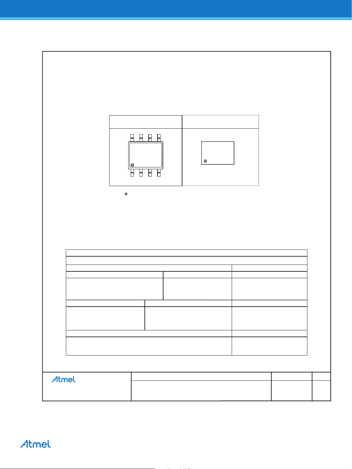
11. Part Markings
AT24CM02: Package Marking Information
8-lead SOIC
ATMLHYWW
## % @
AAAAAAAA
Note 1: designates pin 1
Note 2: Package drawings are not to scale
Catalog Number Truncation
AT24CM02 Truncation Code ##: 2H
Date Codes Voltages
Y = Year WW = Work Week of Assembly % = Minimum Voltage
5: 2015 9: 2019 02: Week 2 M: 1.7V min
6: 2016 0: 2020 04: Week 4 D: 2.5V min
7: 2017 1: 2021 ...
8: 2018 2: 2022 52: Week 52
Country of Assembly Lot Number Grade/Lead Finish Material
@ = Country of Assembly AAA...A = Atmel Wafer Lot Number H: Industrial/NiPdAu
U: Industrial/SnAgCu
Atmel Truncation
ATML: Atmel
8-ball WLCSP
Thin and Standard Thickness Options
ATMLUYWW
## % @
AAAAAA
Package Mark Contact:
DL-CSO-Assy_eng@atmel.com
TITLE
24CM02SM, AT24CM02 Package Marking Information
AT24CM02 [DATASHEET]
Atmel-8828E-SEEPROM-AT24CM02-Datasheet_012017
DRAWING NO.
24CM02SM
4/7/2016
REV.
F
19
Page 20

12. Packaging Information
12.1 8S1 — 8-lead JEDEC SOIC
C
1
N
TOP VIEW
e
D
b
A
A1
SIDE VIEW
Notes: This drawing is for general information only.
Refer to JEDEC Drawing MS-012, Variation AA
for proper dimensions, tolerances, datums, etc.
E
E1
L
Ø
END VIEW
COMMON DIMENSIONS
(Unit of Measure = mm)
SYMBOL
A – – 1.75
A1 0.10 – 0.25
b 0.31 – 0.51
C 0.17 – 0.25
D 4.90 BSC
E 6.00 BSC
E1 3.90 BSC
e 1.27 BSC
L 0.40 – 1.27
ØØ 0° – 8°
MIN
NOM
MAX
NOTE
20
Package Drawing Contact:
packagedrawings@atmel.com
8S1, 8-lead (0.150” Wide Body), Plastic Gull Wing
Small Outline (JEDEC SOIC)
AT24CM02 [DATASHEET]
Atmel-8828E-SEEPROM-AT24CM02-Datasheet_012017
SWB
3/6/2015
DRAWING NO. REV. TITLE GPC
8S1 H
Page 21

12.2 8U-11 — 8-ball WLCSP
A1 CORNER
SEATING PLANE
C
k 0.20 C
A
B
C
D
TOP VIEW
k 0.015 (4X)
12 34
A
B
C
D
D
SIDE VIEW
A
A1
PIN ASSIGNMENT MATRIX
1 2 3
n/a
n/a
SCL
n/a
NC = Not Connected
V
CC
WP
n/a
SDA
NC
n/a
n/a
GND
A
E
B
A2
4
n/a
NC
A
n/a
BOTTOM SIDE
43 21
A
B
C
D
d1
d2
v
COMMON DIMENSIONS
(Unit of Measure = mm)
SYMBOL MIN TYP MAX NOTE
A 0.313 0.334 0.355
A1 — 0.094 —
A2 — 0.240 — 3
D Contact Atmel for details
d1 1.00 BSC
d2 1.40 BSC
E Contact Atmel for details
2
e 0.50 BSC
e1 2.10 BSC
b 0.170 0.185 0.200
Note: 1. Dimensions are NOT to scale.
2. Solder ball composition is 95.5Sn-4.0Ag-0.5Cu.
3. Product offered with Back Side Coating.
A1 CORNER
e1
e
d0.015 C
d
m
m
0.05 C A B
Package Drawing Contact:
packagedrawings@atmel.com
TITLE GPC
8U-11, 8-ball 4x4 Array, Custom Pitch
Wafer Level Chip Scale Package (WLCSP) with BSC
GEN
AT24CM02 [DATASHEET]
Atmel-8828E-SEEPROM-AT24CM02-Datasheet_012017
DRAWING NO.
8U-11 E
8/7/15
REV.
21
Page 22

12.3 8U-18 — 8-ball WLCSP
A1 CORNER
SEATING PLANE
-C-
k 0.20 C
A
B
C
D
TOP VIEW
0.015 (4X)
k
12
A
B
C
D
3
4
D
SIDE VIEW
A
A1
PIN ASSIGNMENT MATRIX
1 2 3
n/a
n/a
SCL
n/a
NC = Not Connected
V
CC
WP
n/a
SDA
NC
n/a
n/a
GND
A
E
A2
4
n/a
NC
A
n/a
BOTTOM SIDE
1
A1 CORNER
e1
e
db
d0.015 C
v
d
0.05 C A B
m
m
43
A
B
C
D
2
d1
d2
COMMON DIMENSIONS
(Unit of Measure = mm)
SYMBOL MIN TYP MAX NOTE
A 0.456 0.495 0.534
A1 — 0.190 —
A2 — 0.305 —
D Contact Atmel for details.
d1 1.00 BSC
d2 1.40 BSC
E Contact Atmel for details.
e 0.50 BSC
2
e1 2.10 BSC
b — 0.270 —
Note: 1. Dimensions are NOT to scale.
2. Solder ball composition is 95.5Sn-4.0Ag-0.5Cu.
22
Package Drawing Contact:
packagedrawings@atmel.com
AT24CM02 [DATASHEET]
Atmel-8828E-SEEPROM-AT24CM02-Datasheet_012017
TITLE GPC
8U-18, 8-ball 4x4 Array, Custom Pitch
Wafer Level Chip Scale Package (WLCSP)
GQA
DRAWING NO.
8U-18 01
4/5/16
REV.
Page 23
13. Revision History
Doc. Rev. Date Comments
8828E 01/2017 Updated Power On Requirements and Reset Behavior section
8828D 05/2016
8828C 11/2015 Corrected 8-ball WLCSP pinout.
8828B 08/2015 Updated the 8U-11 package drawing, data retention discrepancy, and 8-ball pinout.
8828A 05/2015 Initial document release.
Added the 8U-18 standard thickness WLCSP package option. Updated the “Clock and Data
Transition Requirements” section and the “DC Characteristics” table.
AT24CM02 [DATASHEET]
Atmel-8828E-SEEPROM-AT24CM02-Datasheet_012017
23
Page 24

X
Atmel Corporation 1600 Technology Drive, San Jose, CA 95110 USA T: (+1)(408) 441.0311 F: (+1)(408) 436.4200 | www.atmel.com
© 2017 Atmel Corporation. / Rev.: Atmel-8828E-SEEPROM-AT24CM02-Datasheet_012017.
Atmel®, Atmel logo and combinations thereof, Enabling Unlimited Possibilities®, and others are registered trademarks or trademarks of Atmel Corporation in U.S. and
other countries. Other terms and product names may be trademarks of others.
DISCLAIMER: The information in this document is provided in connection with Atmel products. No license, express or implied, by estoppel or otherwise, to any intellectual property right
is granted by this document or in connection with the sale of Atmel products. EXCEPT AS SET FORTH IN THE ATMEL TERMS AND CONDITIONS OF SALES LOCATED ON THE
ATMEL WEBSITE, ATMEL ASSUMES NO LIABILITY WHATSOEVER AND DISCLAIMS ANY EXPRESS, IMPLIED OR STATUTORY WARRANTY RELATING TO ITS PRODUCTS
INCLUDING, BUT NOT LIMITED TO, THE IMPLIED WARRANTY OF MERCHANTABILITY, FITNESS FOR A PARTICULAR PURPOSE, OR NON-INFRINGEMENT. IN NO EVENT
SHALL ATMEL BE LIABLE FOR ANY DIRECT, INDIRECT, CONSEQUENTIAL, PUNITIVE, SPECIAL OR INCIDENTAL DAMAGES (INCLUDING, WITHOUT LIMITATION, DAMAGES
FOR LOSS AND PROFITS, BUSINESS INTERRUPTION, OR LOSS OF INFORMATION) ARISING OUT OF THE USE OR INABILITY TO USE THIS DOCUMENT, EVEN IF ATMEL HAS
BEEN ADVISED OF THE POSSIBILITY OF SUCH DAMAGES. Atmel makes no representations or warranties with respect to the accuracy or completeness of the contents of this
document and reserves the right to make changes to specifications and products descriptions at any time without notice. Atmel does not make any commitment to update the information
contained herein. Unless specifically provided otherwise, Atmel products are not suitable for, and shall not be used in, automotive applications. Atmel products are not intended,
authorized, or warranted for use as components in applications intended to support or sustain life.
SAFETY-CRITICAL, MILITARY, AND AUTOMOTIVE APPLICATIONS DISCLAIMER: Atmel products are not designed for and will not be used in connection with any applications where
the failure of such products would reasonably be expected to result in significant personal injury or death (“Safety-Critical Applications”) without an Atmel officer's specific written
consent. Safety-Critical Applications include, without limitation, life support devices and systems, equipment or systems for the operation of nuclear facilities and weapons systems.
Atmel products are not designed nor intended for use in military or aerospace applications or environments unless specifically designated by Atmel as military-grade. Atmel products are
not designed nor intended for use in automotive applications unless specifically designated by Atmel as automotive-grade.
X
X
XXX
 Loading...