

Page 1
DAC click
DAC click Manual
ver. 1.00
0 100000 020050
1. Introduction
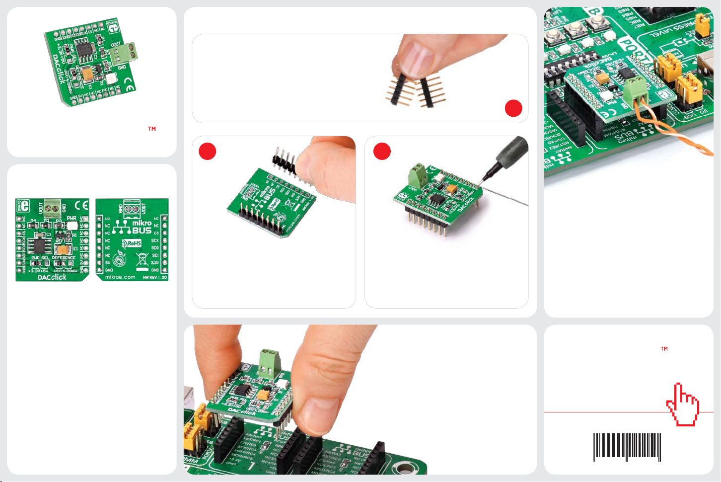
Front and back side appearance
of the DAC click Board
2. Soldering the headers
Before using your click board, make sure
to solder the provided 1x8 male headers
to both sides of the board. Two 1x8 male
headers are included with the board in
the package.
2 3
Turn the board upside down, so that
bottom side is facing you upwards. Place
shorter parts of the header pins in the
both soldering pad locations.
1
Turn the board upward again. Make sure
to align the headers so that they are
perpendicular to the board, then solder the
pins carefully.
4. Creating Output Voltages
Board contains two analog output screw
terminals: Vout and GND. Data in 12-bit
format is sent to the DAC using SPI
communication interface. This data is
converted to the appropriate voltage level
in the range between GND and REFERENCE
(VCC or 4.096V), which is proportional to the
received 12-bit number.
DAC Click is an accessory board in mikroBus™
form factor. It includes a 12-bit Digital-toAnalog Converter MCP4921 that features
SPI interface and an optional double buered
output. The board provides high accuracy
and low noise performance for industrial
applications where calibration or compensation
of signals, such as temperature, pressure and
humidity, are required. Board is set to use
3.3V power supply by default. Solder PWR
SEL SMD jumper to 5V position if used with
5V systems.
3. Plugging the board in
Once you have soldered the headers your
board is ready to be placed into desired
mikroBUS™ socket. Make sure to align the
cut in the lower-right part of the board
with the markings on the silkscreen at the
mikroBUS™ socket. If all the pins are aligned
correctly, push the board all the way
into the socket.
click
BOARD
www.mikroe.com
Page 2
CS#
AN
RST
CS
SCK
MOSI
MISO
+3.3V
GND
PWM
INT
RX
TX
SCL
SDA
+5V
GND
123
J2
VCC
+5V+3V3
R3
2K2
VCC
PWR
VCC
C1
100nF
1
2
3
VIN
VOUT
VSS
REF1
MCP1541
E1
10uF
R1
100
4.096V
NOTE: 4.096V reference can be used only when
5V power supply is provided to the board
VCC
VREF
VCC-REF
VCC-REF
VCC
1
2
3
J1
SCK
SDI
1
2
3
5
4
6
7
8
VDD
CS
SCK
SDI
VREF
LDAC
GND
VOUT
U1
MCP4921
CN2
R2
10K
R4
100K
CS#
SCK
SDI
VCC
VREF
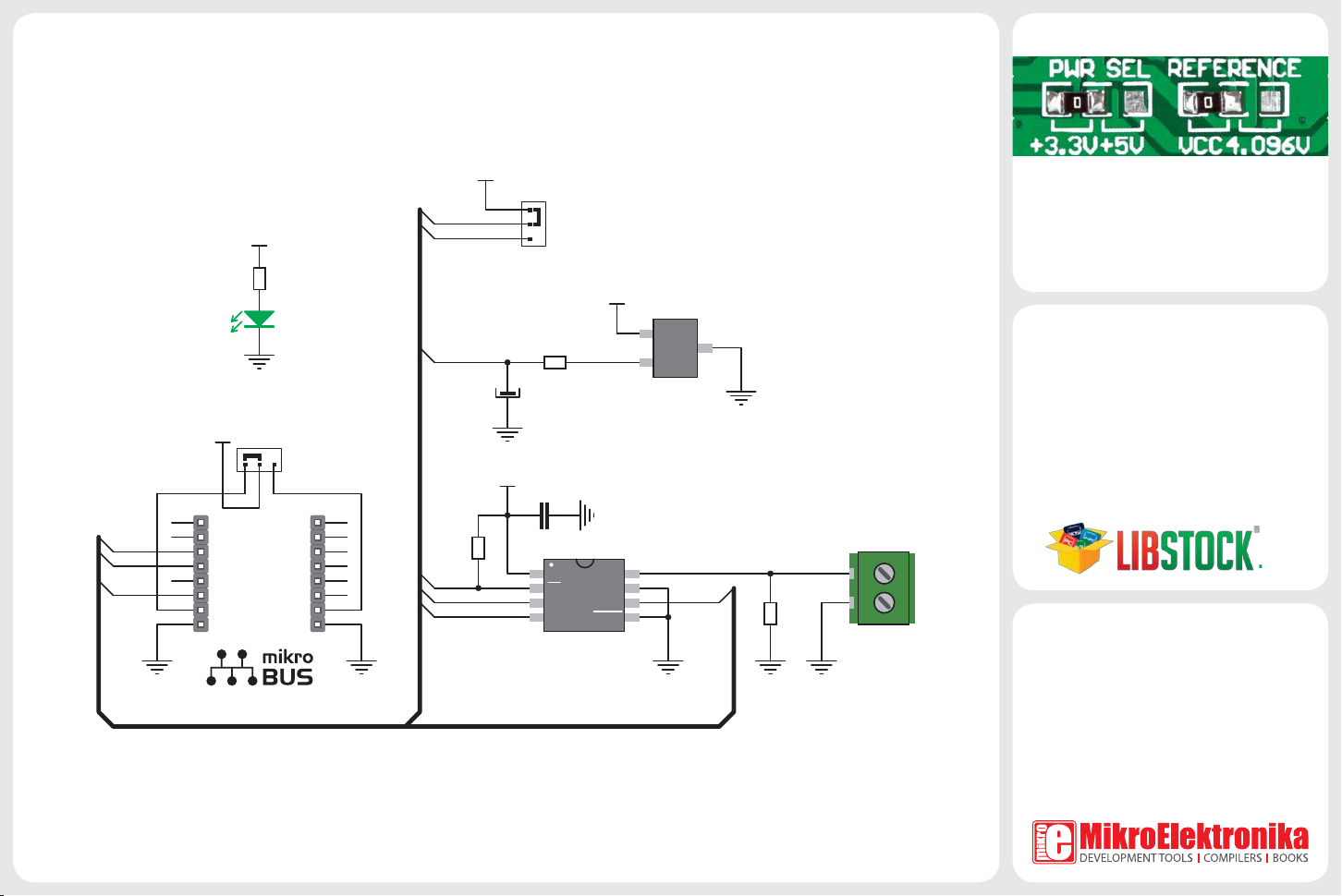
5. DAC click Board Schematics
6. SMD Jumpers
There are two zero-ohm resistors (SMD
jumpers): PWR SEL is used to determine
whether 5V or 3.3V power supply is used, and
REFERENCE to select either VCC or 4.096V as
the voltage reference.
Specication and information contained in the present schematic are subject to change at any time without notice. Copyright © 2012 MikroElektronika. All rights reserved.
MikroElektronika assumes no responsibility or liability for any errors or inaccuracies that may appear in the present document.
7. Code Examples
Once you have done all the necessary
preparations, it’s time to get your click
board up and running. We have provided
the examples for mikroC, mikroBasic and
mikroPascal compilers on our Libstock
website. Just download them and you are
ready to start.
.com
8. Support
MikroElektronika oers Free Tech Support
(www.mikroe.com/esupport) until the
end of product lifetime, so if something goes
wrong, we are ready and willing to help!
 Loading...