

Page 1
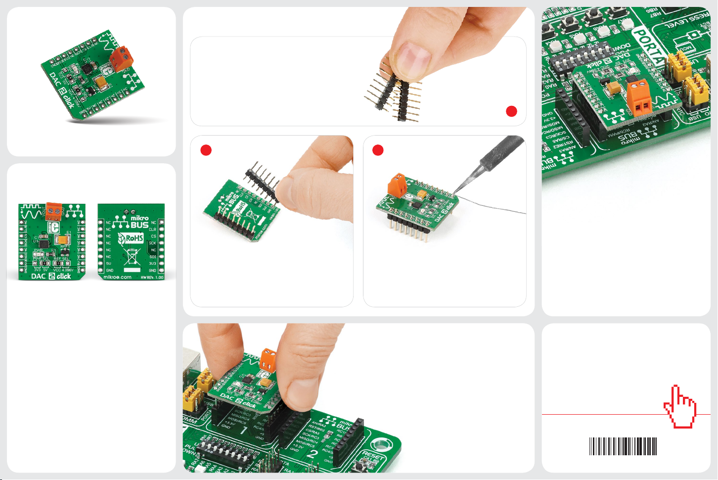
2. Soldering the headers
™
Before using your click board
to solder 1x8 male headers to both left and
right side of the board. Two 1x8 male headers
are included with the board in the package.
, make sure
1
DAC 2 click
1. Introduction
DAC 2 click carries LTC2601CDD, a 16-bit
digital-to-analog converter, along with volt-
age output screw terminals. The chip has high
rail-to-rail output drives (±15mA, Min) and
double-buered data latches. The click board
communicates with the target MCU through
the mikroBUS™ SPI interface (MISO, MOSI
pins) with clock rates up to 50MHz. Addition-
ally, the CLR pin, in place of default mikroBUS™
RST pin, clears all the registers. The board
uses either a 3.3V or 5V power supply.
2 3
Turn the board upside down so that
the bottom side is facing you upwards.
Place shorter pins of the header into the
appropriate soldering pads.
Turn the board upward again. Make sure
to align the headers so that they are
perpendicular to the board, then solder the
pins carefully.
3. Plugging the board in
Once you have soldered the headers your
board is ready to be placed into the desired
mikroBUS™ socket. Make sure to align the cut
in the lower-right part of the board with the
markings on the silkscreen at the mikroBUS™
socket. If all the pins are aligned
correctly, push the board all the
way into the socket.
4. Essential features
DAC 2 click contains two analog output screw
terminals: Vout and GND. 16-bit data is sent
to the DAC through SPI. The digital value is
converted to the appropriate voltage level
in the range between GND and REFERENCE
(VCC or 4.096V), which is proportional to the
received 16-bit number.
click
™
BOARD
www.mikroe.com
DAC 2 click manual
ver 1.00
0100000085011
Page 2
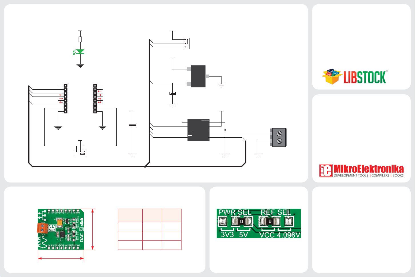
5. Schematic
8. Code examples
CLR
CS
SCK
MOSI
VCC
R1
4K7
PWR
GND
AN
PWM
RST
CS
SCK
MISO
MOSI
+3.3V
GND
MIKROBUS
DEVICE
CONN.1
VCC
POWER SELECTOR
INT
SCL
SDA
+5V
GND
VCC
VREF
VCC-REF
VCC
VCC-REF
TX
RX
VCC
C1
GNDGND
100nF
GND
MOSI
SCK
CLR
CS
E1
10uF
GND
VCC
4.096V
REF1
1
VIN
2
VOUT
MCP1541
U1
1
SDO
2
SDI
3
SCK
4
CLR
5
CS/LD
LTC2601CDD
GND
LDAC
VCC
GND
VOUT
VREF
3
GND
VCC
10
9
8
7
6
VREF
GND
VOUT
CN1
GND
Once you have done all the necessary
preparations, it’s time to get your click board™
up and running. We have provided examples
for mikroC™, mikroBasic™ and mikroPascal™
compilers on our Libstock website. Just
download them and you are ready to start.
.com
9. Support
MikroElektronika oers free tech support
(www.mikroe.com/support) until the end of
the product’s lifetime, so if something goes
wrong, we’re ready and willing to help!
6. Dimensions
28.6 mm / 1125 mils
25.4 mm / 1000 mils
LENGTH
WIDTH
HEIGHT*
* without headers
mm mils
28.6 1125
25.4 1000
10.15 400
7. SMD jumpers 10. Disclaimer
MikroElektronika assumes no responsibility
or liability for any errors or inaccuracies
that may appear in the present document.
Specication and information contained in
the present schematic are subject to change
DAC 2 click features two SMD jumpers: PWR
SEL for switching between a 3.3V or a 5V
power supply, and REF SEL for choosing
either VCC or 4.096V as a reference voltage.
at any time without notice.
Copyright © 2015 MikroElektronika.
All rights reserved.
 Loading...