

Page 1

E a s y P I C v 8
D E V E L O P M E N T B O A R D
U S E R M A N U A L
P A G E 1
E a s y P I C v 8 M a n u a l
Page 2

P A G E 2
It’s time to rethink the way you approach rapid prototyping
Let us introduce you to the latest generation of Mikroe development boards – E a s y P I C v 8
Time saving embedded tools
E a s y P I C v 8 M a n u a l
Page 3

Table of contents
Introduction 5
Development board overview 6
Power supply unit 8
Detailed description 8
Voltage reference 9
Programming voltage 9
PSU connectors 10
Power/debug, USB-C connector 10
Power 12VDC, external power supply 10
Battery power supply 11
Power redundancy and uninterrupted power supply (UPS) 12
Powering up the development board 12
Dual power supply 12
CODEGRIP – programmer/debugger module 14
Device setup 15
PGC/PGD switches 15
DBG selection 15
Connectivity 16
MCU sockets 18
How to properly install the MCU into the DIP socket? 18
VCAP and VCC 19
Crystal oscillator 19
INPUT/OUTPUT section 20
PORT buttons 20
BUTTONS PRESS LEVEL switch 20
UP-PULL-DOWN switch 20
PORT LEDs 20
2x5 pin headers 21
1x20 GLCD graphical display connector 22
1x16 LCD character display connector 25
mikroBUS
Click boards
Communication 28
USB-UART 28
CAN 28
USB ON DEVICE 30
Additional GNDs 31
What’s Next? 34
™
sockets 26
™
27
All images shown in the manual are for illustration purpose only.
Page 4
P A G E 4
E a s y P I C v 8 M a n u a l
Page 5

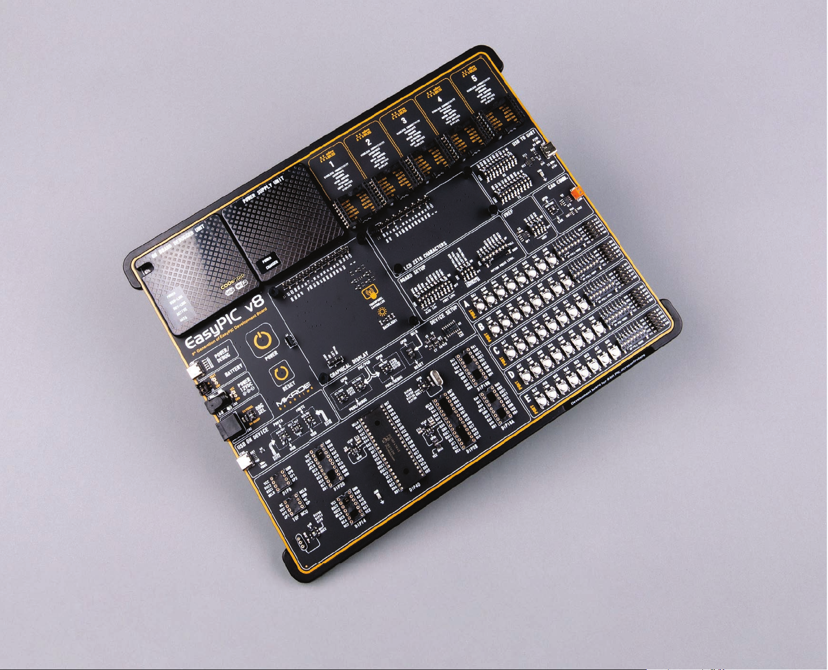
The EasyPIC v8 is a development board designed for the rapid
EasyPIC v8 off ers two display options, allowing even the basic 8-bit PIC
development of embedded applications, based on 8-bit PIC
microcontrollers (MCUs). Redesigned from the ground up, EasyPIC v8
off ers a familiar set of standard features, as well as some new and
unique features, common for the 8th generation of development
boards: programming and debugging over the WiFi network,
connectivity provided by USB-C connectors, support for a wide range
of diff erent MCUs, and more.
The development board is designed so that the developer has everything
that might be needed for the application development, following the
Swiss Army knife concept: a highly advanced programmer/debugger
module, a reliable power supply module, a huge set of connectivity
options including USB (DEVICE), USB to UART, CAN, etc.
EasyPIC v8 board off ers a number of diff erent DIP sockets, covering a
wide range of 8-bit PIC MCUs, from the smallest PIC MCU devices with
only 8 pins, all the way up to 40-pin "giants".
The development board supports the well-established mikroBUS
™
MCU devices to utilize them and display graphical or textual content.
One of them is the 1x20 graphical display connector, compatible with
the familiar Graphical Liquid Crystal Display (GLCD) based on the
KS108 (or compatible) display driver, and EasyTFT board that contains
TFT Color Display MI0283QT-9A, which is driven by ILI9341 display
controller, capable of showing advanced graphical content. The other
option is the 2x16 character LCD module, a four-bit display module
with the embedded character-based display controller, which requires
minimal processing power from the host MCU for its operation.
There is a wide range of useful interactive options at the disposal:
high-quality buttons with selectable press levels, LEDs, pull-up/pull-
down DIP switches, and more. All these features are packed on a
single development board, which itself uses innovative manufacturing
technologies, delivering fl uid and immersive working experience. The
EasyPIC v8 development board is also an integral part of the Mikroe
rapid development ecosystem. Natively supported by the Mikroe
Software toolchain, backed up by hundreds of diff erent Click board
™
designs with their number growing on a daily basis, it covers many
P A G E 5
connectivity standard, off ering fi ve mikroBUS™ sockets, allowing
access to a huge base of Click boards
E a s y P I C v 8 M a n u a l
™
.
diff erent prototyping and development aspects, thus saving precious
development time.
Page 6
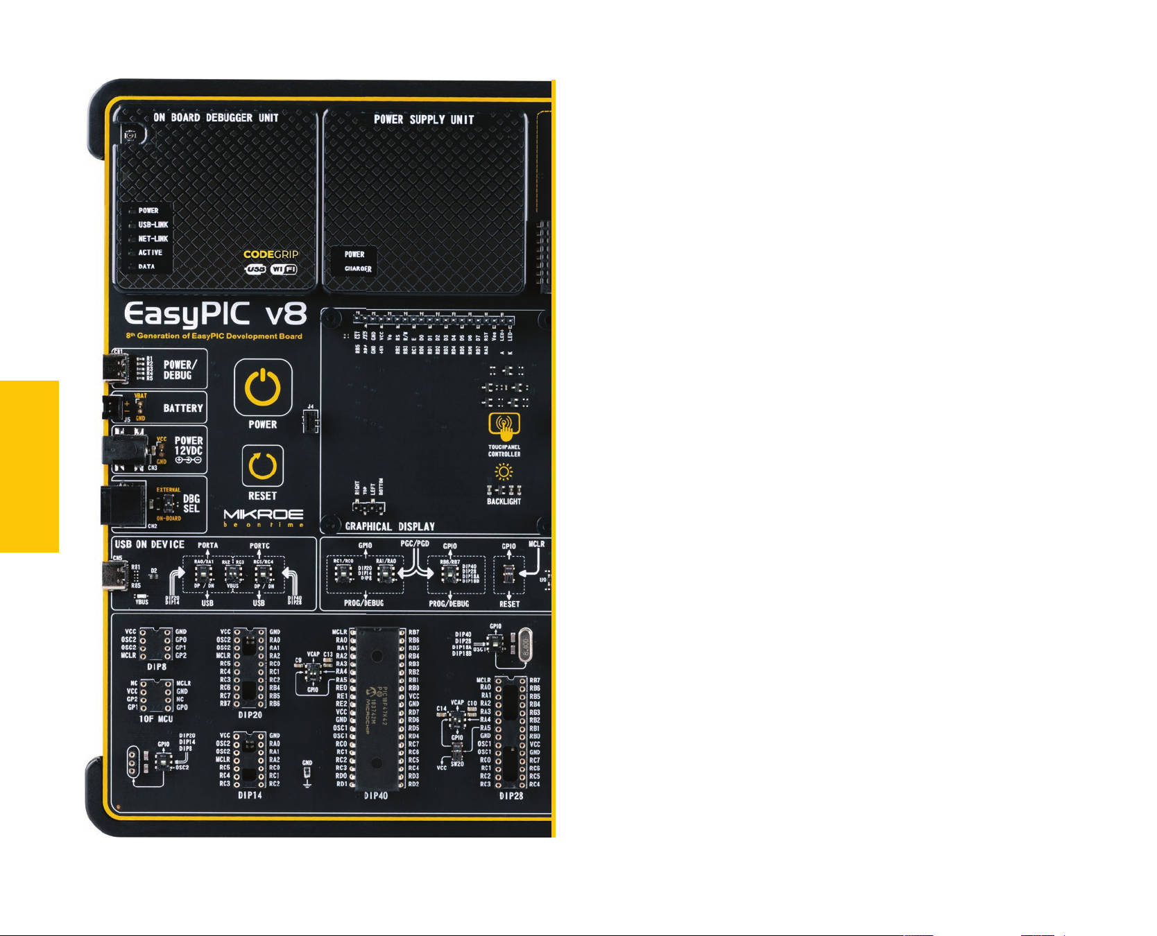
O V E R V I E W
P A G E 6
Development
board overview
The EasyPIC v8 development board features a clean and intuitive layout, allowing the
user to instantly understand how to set it up and how to easily tune it according to
needs. The development board is divided into several sections, arranged so that all the
related interactive components such as switches, buttons, indicators, and connectors,
are logically positioned and grouped together.
Each section of the development board contains components important for reliable
operation of the board itself. The Power Supply Unit (PSU), the CODEGRIP programmer/
debugger module, and fi ve mikroBUS™ sockets are located at the upper section of
the development board. This is where the MCU is powered from, programmed, and
interfaced with various Click boards
The PSU module provides a clean and well-regulated voltage for the development
board. It can use a wide range of external power sources, including a battery, an
external 12V power supply, and a power source over the USB-C connector. It supports
the power supply redundancy function (power ORing) for uninterrupted operation.
The onboard PSU module regulates, fi lters, and distributes the power across all the
connected peripherals. The development board is equipped with two touch-sensitive
buttons labeled as POWER and RESET. These buttons are used to power up the board
and reset the MCU. Their sleek design and fl awless responsiveness add up to the whole
experience. These touch-sensitive buttons are resistant to wear over time and do not
exhibit any bouncing eff ect, unlike mechanical switches.
™
.
The powerful CODEGRIP module, an integrated programmer/debugger module
supports a wide range of diff erent 8-bit PIC MCUs, produced by Microchip. It allows
in-place programming and debugging of all the supported MCUs, off ering many
useful programming/debugging options and seamless integration with the Mikroe
software environment. It also off ers some powerful and unique features such as the
programming/debugging over WiFi; a feature that will revolutionize the way that the
embedded applications are developed.
The CODEGRIP module uses the USB-C connector for a reliable and secure connection
with the personal computer (host PC). It does not require any additional drivers
because it utilizes a HID driver model, natively supported by the computer's operating
E a s y P I C v 8 M a n u a l
Page 7

system (OS). The USB-C connector is also used to power the development board,
simplifying the cable management.
The EasyPIC v8 development board off ers fi ve improved mikroBUS
™
sockets,
allowing interfacing with a vast amount of electronic circuits and reference designs,
standardized under the Click board trademark. Click boards
™
are simple to use, require
no additional hardware confi guration and can be easily connected to the development
board by inserting them into any of the available mikroBUS
of the mikroBUS
™
socket allows even easier interfacing with the Click board™ line
of products: it has a sturdier design which helps to align the Click board
™
sockets. A new design
™
correctly.
To read more about development improvements and huge benefi ts off ered by the
mikroBUS
™
and Click board™ line of products, visit the offi cial Mikroe web page at
www.mikroe.com
The EasyPIC v8 development board is equipped with two display connectors, located
in the middle section of the board. One connector is a 1x16 pin header used for
connecting a character-based LCD in 4-bit mode. The second display connector is a
single row 20 pin header, which supports monochromatic GLCD and EasyTFT board.
The 1x20 pin graphical display connector is accompanied by two 4-pin connectors
(4-pin FFC connector and 1x4 pin header), which are used for the touch panel
connection. The development board also provides the required circuitry, allowing the
resistive touch panel to be interfaced with the installed MCU. Both the LCD and GLCD
display connectors support a PWM-driven (dimmable) or fi xed backlight functionality.
The I/O section occupies the lower part of the development board and contains
available MCU pins routed to 2x5 pin headers for easy access. There are confi gurable
pull-up or pull-down resistors and buttons for applying logic states to MCU pins.
LED indicators provide visual feedback of logic states for each pin. The MCU pins are
divided into groups, following the grouping concept used on the MCU itself (PORTA,
PORTB, PORTC, PORD and PORTE). The I/O section is where the most interaction with
the MCU takes place.
O V E R V I E W
P A G E 7
Communication options such as USB-UART, USB (DEVICE) and CAN are also included.
All the connectors are positioned at the edges of the development board, so they can
be easily accessed. This is also true for the power connectors, as well as for an external
RJ12 ICD connector. This allows clean and clutter-free cable management.
The EasyPIC v8 development board is equipped with the onboard CODEGRIP module
and supported by a powerful CODEGRIP Suite, enabling complete control over the
programming and debugging tasks. It is also used to confi gure various other options
and settings, providing visual feedback through its clean and comprehensive Graphical
User Interface (GUI). Detailed explanation on how to confi gure and use the CODEGRIP
module fi nd at the following link: www.mikroe.com/debuggers/codegrip
E a s y P I C v 8 M a n u a l
Page 8
Power supply unit
The power supply unit (PSU) (1) provides clean and regulated power, necessary for
proper operation of the development board. The host MCU, along with the rest of the
peripherals, demands regulated and noise-free power supply. Therefore, the PSU
is carefully designed to regulate, fi lter, and distribute the power to all parts of the
development board. It is equipped with three diff erent power supply inputs, off ering
all the fl exibility that EasyPIC v8 needs, especially when used on the fi eld. In the case
when multiple power sources are used, an automatic power switching circuit with
predefi ned priorities ensures that the most appropriate will be used.
The PSU also contains a reliable and safe battery charging circuit, which allows a
single-cell Li-Po/Li-Ion battery to be charged. Power OR-ing option is also supported,
providing uninterrupted power supply (UPS) functionality when an external or USB
power source is used in combination with the battery.
1
3
4
Detailed description
The PSU has a very demanding task of providing power for the host MCU and all the
peripherals onboard, as well as for the externally connected peripherals. One of the key
P O W E R S U P P L Y
P A G E 8
P A G E 8
requirements is to provide enough current, avoiding the voltage drop at the output.
Also, the PSU must be able to support multiple power sources with diff erent nominal
voltages, allowing switching between them by priority. The PSU design, based on a
set of high-performance integrated devices produced by Microchip, ensures a very
good quality of the output voltage, high current rating, and reduced electromagnetic
radiation.
At the input stage of the PSU, the MIC2253, a high-effi ciency boost regulator IC
with overvoltage protection ensures that the voltage input at the next stage is wellregulated and stable. It is used to boost the voltage of low-voltage power sources
(a Li-Po/Li-Ion battery and USB), allowing the next stage to deliver well-regulated
3.3V and 5V to the development board. A set of discrete components are used to
determine if the input power source requires a voltage boost. When multiple power
sources are connected at once, this circuitry is also used to determine the input
priority level: externally connected 12V PSU (2), power over USB (3), and the Li-Po/LiIon battery (4). The transition between available power sources is seamless, providing
uninterrupted operation of the development board.
2
(1) This image is only for demonstration purpose, please do not
remove the PSU plastic cover nor touch any of the components
below. The development board can be permanently damaged.
E a s y P I C v 8 M a n u a l
E a s y P I C v 8 M a n u a l
Page 9
Figure 1: Power supply unit view
The next PSU stage uses two MIC28511, synchronous step-down (buck) regulators,
capable of providing up to 3A at their output. The MIC28511 IC utilizes the HyperSpeed
Control® and HyperLight Load® architectures, providing an ultra-fast transient
response and high effi ciency for light loads. Each of the two buck regulators is used
to supply power to the corresponding power supply rail (3.3V and 5V), throughout the
entire development board and connected peripherals.
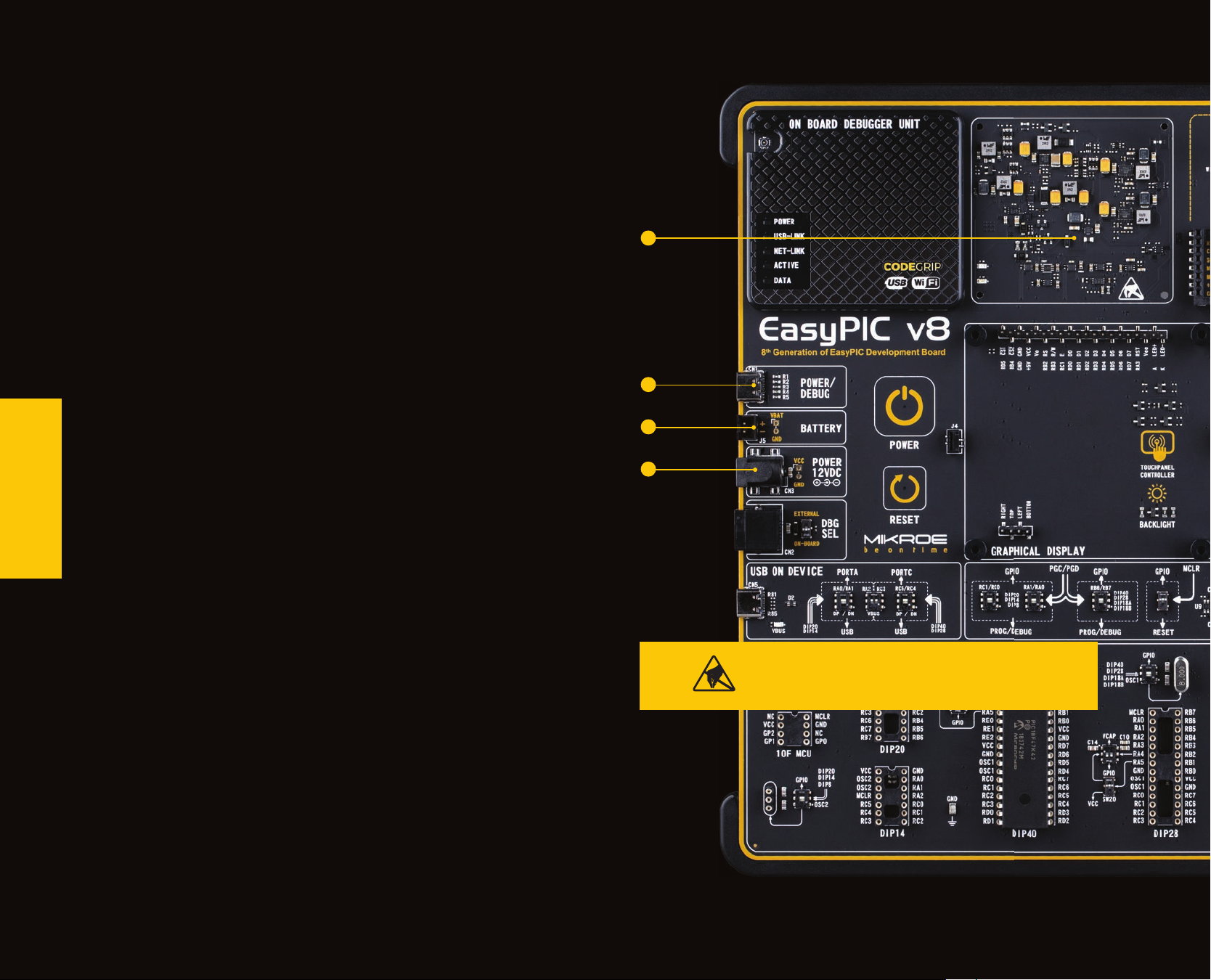
Voltage reference
The PSU is able to provide a very accurate, programmable voltage reference (VREF) (5)
in the range from 0V to 4.096V. VREF is very useful for many diff erent applications
including A/D and D/A converters, comparators, etc.
The programmable VREF design is based on several diff erent ICs produced by
Microchip: the MCP1501, a high-precision buff ered voltage reference IC is used to
provide a very precise VREF of 4.096V for the MCP4726, a 12-bit D/A converter (DAC)
with integrated EEPROM. The MCP4726 DAC is controlled and programmed by the
CODEGRIP module, over the I2C interface. Finally, the MCP606, a single rail-to-rail
operational amplifi er is used to provide an additional buff ering at the output. By using
5
a 4-pole DIP switch (6) located in the VREF section of the development board, it is
possible to route VREF to four diff erent MCU pins:
6
ON (up): connects VREF to the MCU pins (RA0, RA1, RA3, and RC0)
OFF (down): disconnects VREF from the MCU pins (RA0, RA1, RA3, and RC0)
P O W E R S U P P L Y
Programming voltage
P A G E 9
P A G E 9
Not all PIC MCU devices support low voltage programming. Therefore, the PSU module
has to provide the required high voltage (VPP) for the programming of such devices.
The VPP is controlled by the CODEGRIP module automatically, it depends on the
programmed MCU and can’t be modifi ed by the user. To provide a suffi cient voltage
level, the MIC2250, a high-effi ciency, low EMI boost regulator is used. It is used to
provide 14V for the operational amplifi er circuit composed of a dual operational
amplifi er, labeled as MCP6H02T, and produced by Microchip. This circuit has a fi xed
gain, allowing the CODEGRIP programmer/debugger module to reach up to 14V for
the high-voltage programming of various PIC MCU devices.
N O T EIn order to protect host MCU and development board, VREF values higher then
3.3V can only be set if the board voltage is previously set to 5V.
E a s y P I C v 8 M a n u a l
E a s y P I C v 8 M a n u a l
Page 10

PSU connectors
As explained, the advanced design of the PSU allows several types of power sources to
be used, offering unprecedented flexibility: when powered by a Li-Po/Li-ION battery,
it offers an ultimate degree of autonomy. For situations where the power is an issue,
it can be powered by an external 12VDC power supply, connected over the 5.5mm
barrel connector. Power is not an issue even if it is powered over the USB cable. It can
be powered over the USB-C connector, using power supply delivered by the USB HOST
(e.g. personal computer), USB wall adapter, or a battery power bank.
There are three power connectors available, each with its unique purpose:
POWER/DEBUG, USB-C connector
BATTERY, standard 2.5mm pitch XH battery connector
POWER 12VDC, barrel type male 2mm x 6.5mm power connector
Power/debug, USB-C connector
The development board can be powered over the USB-C connector, labeled as POWER/
P O W E R S U P P L Y
DEBUG. This connector provides power from the USB host, USB power bank, or USB
wall adapter. When powered over the USB connector, the available power will depend
on the USB power source capabilities.
When using a PC as a power source, the maximum power can be obtained if the host
PC supports the USB 3.2 interface and is equipped with USB-C connectors. If the host
PC has a USB 2.0 interface, it will be able to provide the least power, since only up to
500 mA (2.5W at 5V) is available from the host in that case. Note that when using
long USB cables or USB cables of low quality, the voltage may drop outside the rated
operating voltage range, causing unpredictable behavior of the development board.
N O T EIf the host PC is not equipped with the USB-C connector, a Type A to Type C USB
adapter may be used (included in the package).
Power 12VDC, external power supply
An external 12V power supply can be connected over the 12VDC barrel connector.
When using an external power supply, it is possible to obtain an optimal amount of
power, since one external power supply unit can be easily exchanged with another,
while its power and operating characteristics can be decided per application. The
development board allows a maximum current of 2.8A per power rail (3.3V and 5V)
when using an external 12V power supply. The barrel-type connector is useful for
connecting wall-adapters.
P A G E 10
Maximum power ratings, along with the allowed input voltage range in the case when
the USB power supply is used, are given in the table below:
USB Power Supply
Input Voltage [V] Output Voltage [V]
MIN
4.4 5.5
Figure 2: USB power supply table
MAX
3.3
3.3 & 5
5
Max Current [A] Max Power [W]
1.8
1.4
0.8 & 0.8
6
7
6.64
Maximum power ratings, along with the allowed input voltage range in the case when
the external power supply is used, are given in the table below:
External Power Supply
Input Voltage [V] Output Voltage [V]
MIN
10.6 14
Figure 3: External Power supply table
MAX
3.3
3.3 & 5
5
Max Current [A] Max Power [W]
2.8
2.8
2.8 & 2.8
E a s y P I C v 8 M a n u a l
9.24
14
23.24
Page 11

N O T E When connecting an external power supply over a barrel connector, make sure
that the polarity of the barrel connector is matched with its counterpart on
the development board, according to the image printed next to the male DC
connector.
Battery Power Supply
Input Voltage [V] Output Voltage [V]
MIN
MAX
3.3
Max Current [A] Max Power [W]
1.6
5.28
Battery power supply
When powered by a single-cell Li-Po/Li-Ion battery, the development board offers an
option to be operated remotely. Combined with the fact that the board can be remotely
programmed and debugged over the WiFi network, the EasyPIC v8 development board
allows complete autonomy, allowing it to be used in some very specific situations:
hazardous environments, agricultural applications, etc.
N O T E It is advised to disable the battery charging circuitry if there is no battery
connected to the EasyPIC v8 development board. This can be done using
CODEGRIP Suite.
The development board uses a 2.5mm pitch XH battery connector. It allows a range
of Li-Po and Li-Ion batteries to be connected. The development board offers battery
charging functionality from both the USB connector and the external power supply.
The battery charging circuitry of the PSU module manages the battery charging
process, ensuring optimal charging conditions and longer battery life. The charging
process is indicated by a CHARGER LED indicator.
5
3.5 4.2
3.3 & 5
Figure 4: Battery Power Supply table
Using USB hubs, long USB cables, and low-quality USB cables, may cause a
significant USB voltage drop, which can obstruct the battery charging process.
1.2
0.7 & 0.7
5.81
6
P O W E R S U P P L Y
The battery charging current can be configured by using the CODEGRIP Suite, which
offers a choice between 100mA and 500mA when the USB power supply is used,
or between 100mA and 200mA when the external 12V power supply is used. In the
case when the development board is powered OFF, the charging current will be set to
500mA by default (200mA with the external power supply).
If both the external 12V power supply and the USB cable are connected to the
development board, the battery will be charged from the external 12V power supply,
thus minimizing the USB power consumption.
Maximum power ratings at a fully charged battery, along with the allowed input
voltage range when the battery power supply is used, are given in the following table:
E a s y P I C v 8 M a n u a l
P A G E 11
Page 12

Power redundancy and uninterrupted
power supply (UPS)
The PSU module supports power supply redundancy: it will automatically switch to
the most appropriate power source if one of the connected power sources fails or
becomes disconnected. The power supply redundancy also allows for an uninterrupted
operation (e.g. UPS functionality, the battery will still provide power if the USB cable is
removed, without resetting the MCU during the transition period).
Powering up the development board
Two touch-sensitive buttons are used to power up and reset the EasyPIC v8
development board. These capacitive buttons are processed by two AT42QT1011,
digital burst mode charge-transfer sensors, specifi cally designed for human-machine
interfaces (HMI), from Microchip. The AT42QT1011 allows very responsive and reliable
touch detection for the connected button pad.
As soon as a valid power source is connected, the development board will enter the
Stand-By mode. When the capacitive POWER button is pressed, the PSU module will
P O W E R S U P P L Y
start distributing the power to the rest of the development board. This is indicated by
the POWER LED indicator, located on the PSU module itself.
GPIO (up): if the MCU uses the MCLR/GPIO pin as the GPIO
RESET (down): if the MCU uses the MCLR/GPIO pin as the MCLR (RESET)
N O T EThe MCLR/GPIO pin should be set via the CONFIG bits as MCLR, and the MCLR switch
should be in the RESET (down) position, in order for the RESET button to work.
Dual power supply
EasyPIC v8 development board supports both 3.3V and 5V power supply on a single
board. Advanced PSU module provides the possibility to chose power supply for board
and host MCU, between 3.3V (default) and 5V. This setting can be easily confi gured
from CODEGRIP Suite, and this feature greatly increases the number of supported
MCUs.
P A G E 12
P A G E 12
Right under the POWER LED, there is a CHARGE LED, indicating the charging status of
the Li-Po/Li-Ion single cell battery, if connected. The complete battery power supply
section, including the battery charger circuit, is explained in the respective chapter
of this manual.
Below the POWER capacitive button (1), there is a RESET capacitive button (2) which
is not entirely power-related, but it has a similar function: it is routed to the MCLR
pin of the MCU, allowing the RESET function to be performed. However, since low pin-
count MCUs often use multiple functions on the same pin, the development board
off ers a choice in the form of a DIP switch (3) labeled as MCLR, which allows to specify
whether the MCLR/GPIO pin should be used as GPIO or it should be connected to the
RESET circuit of the development board:
E a s y P I C v 8 M a n u a l
E a s y P I C v 8 M a n u a l
Page 13

Figure 4: Battery power supply connection
1 2 3
Page 14

1
CODEGRIP
C O D E G R I P
programmer /
debugger module
P A G E 14
P A G E 14
Envisioned as the unifi ed development platform for all the 8-bit PIC MCUs in DIP
package, the EasyPIC v8 development board is equipped with the onboard CODEGRIP
programming/debugging module, to support programming/debugging feature.
The CODEGRIP module can be interfaced with the host computer over the USB-C
connector.
Besides the USB cable, the CODEGRIP module (1) can be accessed over the WiFi
network. This is a revolutionary new feature, which allows some unique usage
scenarios, currently not available on any other programming/debugging solution in
the world. The WiFi connectivity option of the CODEGRIP module off ers a complete
autonomy of the development board. Running in the hazardous environment while
2 34
debugging the software in real time, programming the MCU with a new software
during exposure, having the sensor responses collected and logged remotely from
several diff erent base points, debugging a drone fi rmware while it is in mid-air... These
are just simple examples of what EasyPIC v8 development board can off er.
CODEGRIP module is equipped with LED indicators that provide visual feedback about
its status:
POWER (GREEN) Indicates that the development board is powered on
USB-LINK (YELLOW) After the host OS completes the USB enumeration of the
CODEGRIP module, this LED will indicate that the connection has been established
Figure 5: Programmer/debugger view
E a s y P I C v 8 M a n u a l
Page 15

NET-LINK (AMBER) When the CODEGRIP module is connected to the WiFi network,
this LED will indicate that the connection has been established
If using DIP40, DIP28, DIP18A, or DIP18B MCU sockets, a DIP switch with the RB6/
RB7 label printed above it should be used to confi gure the programming lines:
ACTIVE (RED) Indicates the operational state of the CODEGRIP module: when
CODEGRIP module is in the bootloader mode, this indicator will blink. Normal operation
of the CODEGRIP module is indicated by the ACTIVE LED being constantly turned ON
DATA (BLUE) Indicates that there is a data transfer ongoing between the MCU and the
CODEGRIP module
The onboard CODEGRIP module requires no additional drivers, as it utilizes a HID driver
model, which is natively supported by the computer OS. This makes its installation
very easy and straightforward in the case when the USB cable is used. As soon as the
USB cable is connected to the host PC, the CODEGRIP module is enumerated and the
development board is ready to be used.
CODEGRIP programmer/debugger module is supported by CODEGRIP Suite. Detailed
explanation on how to confi gure and use the CODEGRIP module on the EasyPIC v8
development board fi nd at the following link: www.mikroe.com/debuggers/codegrip
CODEGRIP device setup
Since the development board supports many diff erent MCUs with a diff erent number
of pins and functionalities, it is necessary to connect the CODEGRIP programmer/
debugger to the correct programming lines (PGC, PGD) of the particular MCU. The
development board allows easy selection of the programming lines by off ering a set of
high-quality DIP switches (2), which ensure reliable operation. For more information
about MCU DIP sockets and how to use them, please refer to the MCU sockets chapter.
All DIP switches required to set up the programming and reset lines for each DIP
socket, are grouped under the DEVICE SETUP (3) label, in a section located in the
middle of the EasyPIC v8 development board.
RB6/RB7 (DIP40, DIP28, DIP18A, DIP18B)
GPIO (up): allows the RB6 and RB7 pins to be used as GPIO lines
PROG/DEBUG (down): connects the RB6 and RB7 pins to the CODEGRIP
programmer/debugger module
If using DIP20, DIP14, DIP8 or 10F MCU sockets, two DIP switches are available for
confi guration of the programming lines, depending on a particular MCU that is used:
RA1/RA0 (DIP20, DIP14, DIP8,10F MCU)
GPIO (up): allows the RA1 and RA0 pins to be used as GPIO lines
PROG/DEBUG (down): connects the RA1 and RA0 pins to the CODEGRIP
programmer/debugger module
RC1/RC0 (DIP20, DIP14, DIP8,10F MCU)
GPIO (up): allows the RC1 and RC0 pins to be used as GPIO lines
PROG/DEBUG (down): connects the RC1 and RC0 pins to the CODEGRIP
programmer/debugger module
DBG selection
The EasyPIC v8 development board is equipped with the RJ-12 connector (4),
compatible with Microchip® ICD external programmers/debuggers. If an external
programmer/debugger is connected, the onboard CODEGRIP module should be
disabled to avoid data corruption. A DIP switch located next to RJ-12 ICD connector
allows selection of a programmer/debugger that will be used:
EXTERNAL (up): an external programmer/debugger is connected, the onboard
CODEGRIP module is disabled
ONBOARD (down): an external programmer is not connected, the
onboard CODEGRIP module is enabled
C O D E G R I P
P A G E 15
P A G E 15
PGC/PGD switches
There are three switches located in the DEVICE SETUP section, labeled as PGC/PGD. These
switches allow to redirect the programming lines of the CODEGRIP onboard module to the
corresponding programming pins of the MCU. These switches have an MCU DIP socket name
printed next to it, so it is very easy to know which one should be used for which socket.
E a s y P I C v 8 M a n u a l
Page 16

Connectivity
One of the key features of the EasyPIC v8 development board is its connectivity.
It features a diversity of connecting options making the board very versatile, adaptable to any situation, and very easy
to work with.
The EasyPIC v8 development board supports all 8-bit PIC MCUs in DIP package type. To allow this, the development
board off ers a total of eight DIP socket sizes: DIP8, DIP14, DIP18 (A, B), DIP20, DIP28, DIP40 and an additional DIP8
socket for 10F MCU families.
The development board also features two display connectors (1x16 character display connector and 1x20 graphical
display connector), USB-UART, an external ICD compatible programmer/debugger connector and more. The PORT I/O
section is the most distinctive connectivity option. It allows direct interfacing with the MCU pins. This section also
contains LEDs for visual indication of pin states, BUTTONs for applying the desired logic states to the pins, and DIP
switches for confi guring pull-up or pull-down resistors.
C O N N E C T I V I T Y
CONNECTIVITY
P A G E 16
All LEDs, buttons, and headers are logically organized and grouped as PORTs, following the pin organization topology
of the MCU itself.
Availability of fi ve standardized mikroBUS
special: the world of Click boards
virtually an unlimited number of combinations is possible, considering the fact that the Click board
already has several hundreds of various Click boards
EasyPIC v8 development board with the whole Mikroe ecosystem, allows seamless and eff ortless prototyping, and
truly rapid embedded application development. For more info about the mikroBUS
of products, please visit the offi cial Mikroe web page at: www.mikroe.com
™
sockets is something that makes the EasyPIC v8 development board very
™
is now just under your fi ngertips. By combining up to 5 diff erent Click boards™,
™
repository
™
, with more added on a daily basis. Tight integration of the
™
standard and the Click board™ line
E a s y P I C v 8 M a n u a l
Page 17

Easily create an IoT Weather Station with the EasyPIC v8 development board.
Use the following tools:
EasyPIC v8 development board
EasyTFT board
G2C click
OLED C click
Temp-Log 2 click
Thunder click
LPS22HB click
E a s y P I C v 8 M a n u a l
C O N E C T I V I T Y
P A G E 17
Page 18

Figure 6: Main board with MCU socket section view
MCU sockets
As previously mentioned, the EasyPIC v8 development board supports all 8-bit PIC
MCUs in DIP package type. There are eight diff erent sockets, ranging from DIP8 (8-pin
DIP socket), up to DIP40 (40-pin DIP socket). All DIP sockets are grouped in the lower
left area of the board (1).
Only a single DIP socket should be populated at a time since their lines are shared.
Each DIP socket allows an MCU with the specifi c pin-count to be used. For example, if
using a 40-pin MCU, it should be placed into the DIP40 socket, exclusively (i.e. placing
an 8-pin MCU into the DIP14 socket will cause pin misalignment and other problems).
However, there are exceptions to this rule: if using an MCU in DIP18 package type,
there are two options available, depending on its pinout: DIP18A and DIP18B. To
determine the correct socket that should be used in this case, the pinout of the MCU
should be compared with the pinout which is printed next to these sockets.
P A G E 18
A similar exception applies to the DIP8 socket: if using an 8-pin MCU from PIC10F
MCU families, it should be installed in the 10F MCU socket instead of the DIP8 socket.
How to install the MCU into the DIP socket?
First make sure that a half circular cut in the microcontroller DIP packaging matches
the cut in the DIP socket (2). Align both ends of the microcontroller with the socket.
Then put the microcontroller slowly down until all the pins match the socket. Check
again if everything is placed correctly and gently press the microcontroller until it is
completely plugged into the socket.
Only a single MCU must be installed into the development board at a time.
29 64108
51 3 7
E a s y P I C v 8 M a n u a l
Page 19

Crystal oscillator
VCAP and VCC
Most of PIC MCU devices can use an external quartz-crystal oscillator. There are two
sockets for installing the crystal oscillator, depending on which MCU socket will be
used:
Crystal oscillator socket OSC1 is routed to DIP40, DIP28, DIP18A, and DIP18B MCU sockets (7)
Crystal oscillator socket OSC2 is routed to DIP20, DIP14, and DIP8 MCU sockets (8)
10F MCUs do not use external oscillators. Consequently, none of the crystal oscillator
socket pins are routed to the 10F MCU DIP socket.
Above the DIP28 MCU socket, there is a DIP switch (9) used to specify whether the
OSC1/RA6 and OSC1/RA7 pins will be used as GPIOs on the corresponding MCU
sockets, or connected to the OSC1 crystal oscillator socket:
RA6, RA7 (OSC1)
UP position: allows the RA6 and RA7 pins to be used as GPIO lines
DOWN position: connects the RA6 and RA7 pins to the crystal oscillator socket OSC1
Below the two DIP8 MCU sockets, there is a DIP switch (10) used to specify whether
the OSC2/RA4 and OSC2/RA5 pins will be used as GPIOs on the corresponding MCU
sockets, or connected to the OSC2 crystal oscillator socket:
RA4, RA5 (OSC2)
UP position: allows the RA4 and RA5 pins to be used as GPIO lines
DOWN position: connects the RA4 and RA5 pins to the crystal oscillator socket OSC2
For some of the PIC MCU devices, the manufacturer (Microchip) suggests using
additional bypass capacitors for improved stability. These MCUs use internal
voltage regulators since their cores operate at diff erent (lower) voltages than their
peripherals. For some applications, it may be necessary to use bypass capacitors,
in order to ensure better noise immunity. This applies to DIP40 (2) and DIP28 (3)
sockets. However, the EasyPIC v8 development board off ers a choice, since each pin
on these low pin-count MCUs can be very valuable.
Next to the DIP40 MCU socket, there is a two-pole DIP switch (4) used to specify
whether the VCAP/RA4 and VCAP/RA5 pins will be used as GPIOs on this MCU socket,
or connected to the onboard bypass capacitors:
RA4/RA5 (DIP40)
VCAP (up): connects the RA4 and RA5 pins to the onboard capacitors
GPIO (down): allows the RA4 and RA5 pins to be used as GPIO lines
Next to the DIP28 MCU socket, there is another two-pole DIP switch (5) used to
specify whether the VCAP/RA4 and VCAP/RA5 pins will be used as GPIOs on this MCU
socket, or connected to the onboard bypass capacitors:
RA4/RA5 (DIP28)
VCAP (up): connects the RA4 and RA5 pins to the onboard capacitors
GPIO (down): allows the RA4 and RA5 pins to be used as GPIO lines
Next to the DIP28 MCU socket, there is an additional DIP switch labeled as SW20 (6).
This switch is used if the MCU installed in the DIP28 socket requires an analog voltage
supply (VCC) to be connected:
C O N N E C T I V I T Y
P A G E 19
N O T E 10F MCU families do not use an external crystal oscillator. Consequently, none
of the crystal oscillator socket pins are routed to the 10F MCU DIP socket.
E a s y P I C v 8 M a n u a l
SW20:
UP position: redirects the RA5 pin to be used either as the VCAP or as the GPIO
(depending on the RA4/RA5 DIP switch settings)
DOWN position: Connects the RA5 pin to the power supply rail (for MCUs that
require VCC on this pin)
When using MCU devices that require the analog voltage supply pin to be
connected to the power source (such as PIC18F2331 or PIC18F2431), the
SW20 switch must be in the DOWN position.
Page 20

INPUT/OUTPUT section
I/O pins of any MCU are internally grouped as PORTs. The same grouping concept is
kept throughout the development board as well, off ering a clean and organized user
interface.
There are fi ve PORTs (1) on the EasyPIC v8 development board, labeled from PORTA to
PORTE. Depending on the pin-count of the MCU, not all PORTs will be used. However,
the development board supports the highest pin-count MCUs in DIP package type (40
pins). The PORTs are located at the lower right side of the board, each containing a
set of eight buttons, eight LEDs, an eight-pole DIP switch, and a single 2x5 pin header
with the standard 2.54mm pitch. The PORTs are labeled according to the MCU PORT
they are routed to.
PORT buttons
PORT buttons (2) can be used to apply an arbitrary logic state to the pins of the MCU.
These buttons are small tactile SPST buttons that work in combination with a DIP
switch (SW5), labeled as BUTTONs PRESS LEVEL. This DIP switch is located in the
BOARD SETUP section.
C O N N E C T I V I T Y
P A G E 20
BUTTONs PRESS LEVEL switch
This eight-pole, tri-state DIP switch allows the button to apply a LOW logic level to an
MCU pin when pressed (connecting it to the GND), or to apply a HIGH logic level when
pressed (connecting it to the power rail). It can also be used to completely disconnect
the button, preventing accidental button presses. To limit the pin current and prevent
the excessive inrush of currents when a button is pressed, a protective 220Ω resistor is
used, connected in series with the switch. Each position of the BUTTONs PRESS LEVEL
switch (3) is used to determine the applied logic level of a button press for the entire
PORT. As a result, only fi ve poles of this DIP switch are used, allowing control of all
fi ve groups of buttons (unused poles are marked with the NC label - Not Connected).
BUTTONs PRESS LEVEL:
UP position: a button press applies HIGH logic level to the corresponding PORT pins
MID position: a button is completely disconnected
DOWN position: a button applies LOW logic level to the corresponding PORT pins
UP-PULL-DOWN switch
Besides buttons, each of the fi ve PORTs has an eight-pole DIP switch associated with
it. It is labeled as UP-PULL-DOWN (4) and it is used to enable a pull-up or pull-down
resistor for the specifi c pin or to leave the pin in a fl oating state:
UP-PULL-DOWN:
UP position: connects a 4.7kΩ resistor between the MCU power rail and the pin (the
pin is pulled up)
MID position: Disables both pull-up and pull-down resistor connections from the
pin (the pin is in the fl oating state)
DOWN position: Connects the 4.7kΩ resistor between the GND and pin associated with
the DIP switch position (the pin is pulled down)
PORT LEDs
Each PORT contains a group of eight LEDs (5) used to provide a visual indication
of the logic state of the specifi c pin. The maximum current through a single LED is
limited with the 4.7kΩ resistor. Each LED is connected to a PORT pin and it is labeled
according to the name of the connected pin (RA0 to RE7). LEDs on each PORT should
be disconnected when not used. Having a LED on a communication line or an A/D
converter input might alter expected results since LED represents an additional
electrical load. There is a ten-pole DIP switch (SW6) (6) located in the BOARD SETUP
section. Five poles of this DIP switch, labeled as PORT LEDs are used to enable or
disable LEDs on each PORT:
E a s y P I C v 8 M a n u a l
Page 21

Figure 8: I/O PORTs view
SW6.6 - SW6.10 (PORT LEDS):
UP position: Enables LEDs for a specifi c PORT, associated with the particular DIP
switch position
DOWN position: Disables LEDs for a specifi c PORT, associated with the particular DIP
switch position
C O N N E C T I V I T Y
1 2 65 3 4 7
E a s y P I C v 8 M a n u a l
2x5 pin headers
Besides LEDs, there are also 2x5 pin headers (7) in the PORT sections. All the pins
which belong to a specifi c PORT are routed to the 2x5 pin header located in that PORT
section, along with the GND and the power rails. The pins on these headers are labeled
according to the names of the MCU pins to which they are routed (from RA0-RA7 to
RE0-RE7).
These 2x5 pin headers can be used to expand the connectivity of the EasyPIC v8
development board, allowing interfacing with other devices, peripherals, and
measurement equipment, either by using IDC10 extension cables, IDC10 female
sockets, or simply by using jumper wires. Enhanced connectivity is one of the key
features of the EasyPIC v8 development board, therefore, there are many connectivity
options provided. However, 2x5 pin headers off er the most extensive connectivity
option as they expose all the available MCU pins to the outside world.
P A G E 21
Page 22

1x20 graphical display connector
The EasyPIC v8 development board is equipped with the 1x20 graphical display
connector [1], off ering support for GLCDs with the resolution of 128x64 pixels, driven
by the KS108 or compatible display controller.
Graphical Liquid Crystal Displays (GLCDs) [2] can be used to display monochromatic
graphical content such as text, images, etc. Besides data lines, 1x20 GLCD connector
also contains command lines, necessary power supply rails (GND, +5V for the backlight
and for the display module), backlight PWM control, and contrast control voltage.
GLCDs usually come with a touch-sensitive panel, which allows them to be used as
input devices. The EasyPIC v8 development board provides support for the resistive
touch panel over two separate connectors: one 1x4-pin header and one 4-pin fl at-
cable connector (FFC) labeled as J4 [3], typically used for GLCDs. This connector is
perfectly aligned with the GLCD modules which are available for purchase from the
offi cial Mikroe store. For more information about the GLCD displays, please visit our
web page: www.mikroe.com
Two DIP switches (SW6 and SW2) located in the BOARD SETUP section of the
development board are used to set up the confi gurable options for both the GLCD
backlight and touch panel control. Two poles of the SW6 DIP switch (4), grouped
under the GLCD label, are used to control the backlight options of the GLCD:
C O N N E C T I V I T Y
SW6.1:
ON (up): GLCD backlight is ON
OFF (down): GLCD backlight is OFF
P A G E 22
SW6.2:
ON (up): PWM signal at the RC2 pin controls the GLCD backlight brightness
OFF (down): Backlight brightness amount is fi xed and can't be controlled by the MCU
If you want to upgrade your GLCD application with TFT display, EasyTFT board (5)
is a perfect choice. It features connector compatible with 1x20 graphical display
connector (1) on EasyPIC v8 development board, and a touch panel connector.
The EasyTFT board contains 2.83" TFT color display MI0283QT-9A with 320x240 pixel
resolution, which is driven by ILI9341 display controller, capable of showing advanced
graphical content. Each pixel can display 262K diff erent colors. TFT display is covered
with a resistive touch panel which can be used as input device, supported with 1x4 pin
header [6] on EasyPIC v8 development board.
The board is primarily designed to be used as a display board on Mikroe Easy
development boards. After testing and building the fi nal program, this board can also
be used in your fi nal device. The board also contains mounting holes (7) for easier
integration into your designs.
A four-pole DIP switch (8) labeled as SW2 located in the BOARD SETUP section of the
development board is used to set up the confi gurable options for touch panel control.
It allows to connect the pins RA0, RA1, RA4, and RC0 to the touch panel control circuit:
SW2:
ON (up): A specifi c touch panel control is connected to the respective MCU pin
OFF (down): A specifi c touch panel control is disconnected from the respective MCU pin
The EasyTFT board and LCD use the same pins, thus are unable to operate if
simultaneously plugged in.
N O T E
A four-pole DIP switch (8) labeled as SW2 allows to connect the pins RA0, RA1, RA4,
and RC0 to the touch panel control circuit:
SW2:
ON (up): A specifi c touch panel control is connected to the respective MCU pin
OFF (down): A specifi c touch panel control is disconnected from the respective MCU pin
In order to use backlight PWM dimming, both SW6.1 and SW6.2 switches must
be enabled at the same time.
E a s y P I C v 8 M a n u a l
Page 23

Figure 9: 1x20 pin board connector view
23 4 85 761
E a s y P I C v 8 M a n u a l
E a s y P I C v 8 M a n u a l
C O N N E C T I V I T Y
P A G E 23
Page 24

14 3
2
Figure 10: 1x16 display header view
Page 25

1x16 character display connector
Character-based Liquid Crystal Display (LCD) (1) is a cheap and popular way of
representing application results, short messages, or some other type of information
to users. The EasyPIC v8 development board natively supports 2x16 character LCD
module, connected in 4-bit mode. It off ers a dedicated 1x16 pin header (2) that
can host a compatible LCD module. Each pin of the connector is labeled on the
development board and should be connected to the respective pin of the LCD module.
There are four plastic spacers (3) used to provide physical support for both types of
connected displays (LCD and GLCD), ensuring a reliable connection and preventing
bending of their pins.
The LCD and GLCD use the same pins, thus are unable to operate if simultaneously
plugged in.
Two poles of the SW6 DIP switch (4), grouped under the LCD label, are used to control
the backlight options of the LCD:
SW6.3:
ON (up): LCD backlight is ON
OFF (down): LCD backlight is OFF
N O T E
SW6.4:
ON (up): PWM signal at the RC2 pin controls the LCD backlight brightness
OFF (down): Backlight brightness amount is fi xed and can't be controlled by the MCU
In order to use backlight PWM dimming, both SW6.3 and SW6.4 switches must
be enabled at the same time.
Make sure to turn off the power supply before placing either of the display
modules on the board. Otherwise, the display module or the development board
can be permanently damaged.
C O N N E C T I V I T Y
P A G E 25
Figure 11: EasyTFT board, 1x16 LCD and
Graphic LCD 128x64 with TouchPanel
Page 26

1
™
mikroBUS
sockets
The superior connectivity features of the EasyPIC v8 development board are rounded
up with fi ve standardized mikroBUS
for the board, as it allows interfacing with the vast amount of Click boards
™
mikroBUS
smallest number of pins. More information at www.mikroe.com/mikrobus
is the add-on board standard that off ers maximum expandability with the
™
host connectors (1). It is a considerable upgrade
™
.
P A G E 26
All the mikroBUS
sturdier, allowing a better grip of the Click board
supports between two 8-pin connectors, the right lower edge is chamfered at the
angle of 45°, the same as the Click board
socket. The new mikroBUS™ socket is now a fully-fl edged, standardized monolithic
component with all its pins clearly labeled, off ering very good grip for the Click board
preventing it to fl ip over or to be placed incorrectly.
The mikroBUS
and I2C. There are also single pins reserved for PWM, Interrupt, Analog input, Reset,
and SPI Chip Select. The mikroBUS
(3.3V and 5V), along with the GND pins.
Each MCU socket has the appropriate pins routed to the mikroBUS
Therefore, each mikroBUS
This helps users to identify to which MCU pin its routed to. Also, each mikroBUS
socket is labeled on the development board with its ordinal number, by which the
connector is referenced to in the Mikroe development environment, software
Figure 12: Main board with mikroBUS™ socket close up view
applications, tutorials, etc.
™
sockets are now redesigned and improved. They became much
™
. In addition to added horizontal
™
, making it seamlessly fi t into the mikroBUS
™
socket supports the following communication interfaces: SPI, UART,
™
socket also contains pins with the two power rails
™
sockets.
™
socket pin is clearly labeled on the development board.
E a s y P I C v 8 M a n u a l
™
™
,
™
Page 27

Figure 13: Click boards
™
™
Click boards
THE LARGEST AND FASTEST-GROWING
BASE OF ADD-ON BOARDS IN THE WORLD!
Click boards™ are standardized add-on boards that carry a variety of diff erent electronic
devices. They are designed to perfectly fi t the mikroBUS
the best performances for the used components, they save developers of testing and
troubleshooting often associated with the prototyping phase. They enhance rapid
development and accelerate time to market. These ready-to-use boards require no
additional hardware confi guration. More information at www.mikroe.com/click
™
socket. Engineered to deliver
C O N N E C T I V I T Y
P A G E 27
P A G E 27
E a s y P I C v 8 M a n u a l
Page 28

Communication
COMMUNICATION
P A G E 28
Communication connectors allow the development board to be connected with many
diff erent devices that use high-layer communication protocols such as USB, CAN, etc.
Also, there is a USB-UART converter, which enables simplifi ed communication with the
personal computer over the emulated serial interface. Each of these connectors will be
described in more detail, in the following sections of the manual.
USB-UART
UART (Universal Asynchronous Receiver/Transmitter) interface (1) is one of the most
common interfaces for data exchange between the MCU and other external devices.
The EasyPIC v8 development board off ers the UART connectivity over the USB-C
connector (2) by utilizing the FT230XQ (3), a popular USB-UART signal conversion
IC, produced by FTDI Chip. This IC contains the complete USB stack necessary for the
interface bridging between the UART peripheral of the MCU and the USB interface of
the PC. FT230XQ drivers are available for download from the offi cial FTDI drivers web
page www.ftdichip.com/Drivers/VCP.htm
To enable UART data exchange via the USB-C connector, RX and TX lines of the MCU
UART peripheral must be connected to the corresponding pins of the FT230XQ IC. Two
ten-pole DIP switches located in the USB TO UART section of the board, labeled as TX
(SW21) (4) and RX (SW23) (5), allow fully independent control of the UART RX and TX
lines, off ering complete freedom of pin selection. The TX DIP switch (SW21) connects
the specifi c MCU pin (labeled next to the related switch) as the UART transmission
line, while the RX DIP switch (SW23) connects the specifi c MCU pin (labeled next to
the related switch) as the UART receiving line. This allows custom UART TX/RX pair
confi guration, allowing the development board to adapt to many diff erent UART pin
confi gurations, found on various PIC MCU devices:
SW21 (TX)
ON (up): connects the respective UART TX pin to the USB-UART conversion circuit
OFF (down): disconnects the respective UART TX pin from the USB-UART conversion circuit
SW23 (RX)
ON (up): connects the respective UART RX pin to the USB-UART conversion circuit
OFF (down): disconnects the respective UART RX pin from the USB-UART conversion circuit
UART traffi c is indicated by two LED indicators, located in the USB TO UART section of
the board, near the USB-C connector:
Yellow LED (TX) (6) indicates outgoing data transfer
Red LED (RX) (7) indicates incoming data transfer
CAN
Controller Area Network (CAN or CAN Bus) (8) is a serial network technology, originally
designed for the automotive industry, but due to its robustness and noise immunity,
it has become popular in many other applications. The CAN Bus is primarily used in
embedded systems, allowing to establish fast communication between MCUs or other
peripherals, eliminating the need for expensive and complex technology. The CAN
Bus consists of only two wires, allowing both high data rates and message collision
prevention.
The EasyPIC v8 utilizes the MCP2561FD (9), a high-speed CAN fl exible data rate
transceiver from Microchip, off ering support for both CAN and CAN FD (CAN
Flexible Data Rate) for MCUs equipped with the CAN peripheral. The MCP2561FD
transceiver meets all the automotive requirements for CAN FD, exceeding 2Mbps
data rate, featuring low quiescent current, electromagnetic compatibility (EMC), and
electrostatic discharge (ESD) immunity. Some features provided by the MCP2561FD
include:
∫ Optimized for CAN FD at 2Mbps, 5Mbps, and 8 Mbps operation
∫ CAN Bus Pins are disconnected when the CAN transceiver is unpowered
∫ Detection of ground fault
∫ Protection against damage due to short-circuit conditions
∫ Protection against high-voltage transients in automotive environments
∫ Automatic thermal shutdown
E a s y P I C v 8 M a n u a l
Page 29

11
10
The development board off ers a single DIP switch located in the CAN COMM. section,
which is used to specify whether the RB2 and RB3 pins should be used as GPIOs or
they should be connected to the CAN transceiver circuit as CAN TX and CAN RX lines.
CAN connectivity is provided only for MCUs installed in DIP28 and DIP40 MCU sockets:
RB3/RB2 (DIP28, DIP40) (10)
1
GPIO (up): Allows the RB2 and RB3 pins to be used as GPIOs
CAN (down): Connects the RB2 and RB3 pins to the CAN transceiver circuit
5
7
2
6
3
The development board can be connected to the CAN Bus by using the 2-pole screw
terminal (11), located in the CAN COMM section. Please note that the CAN H and
CAN L diff erential signals need to be properly connected to the CAN Bus, else no CAN
communication will be possible.
4
8
9
COMMUNICATION
Figure 14: Main board partial right side view
E a s y P I C v 8 M a n u a l
P A G E 29
P A G E 29
Page 30

COMMUNICATION
P A G E 30
P A G E 30
USB ON DEVICE
USB (Universal Serial Bus) (1) is a very popular industry standard that defi nes cables,
connectors, and protocols used for communication and power supply between
devices. USB-C connector (2) is the latest version of the USB connector, developed
by the USB Implementation Forum (USB-IF). Due to its many advantages including
symmetrical pinout, higher current capacity, and support for faster data rates, it
off ers a signifi cant improvement over the previous versions. This allows MCU devices
equipped with the USB peripheral to connect to an external USB HOST (such as a PC,
Laptop, etc.), allowing the development of USB-based applications. The connection to
the USB HOST is indicated by a yellow LED labeled as VBUS (3), located in the USB ON
DEVICE section, near the USB-C connector.
When a PIC MCU does not support USB interface or USB connection is not required by
application itself, the USB pins should be disconnected from the USB-C connector and
accompanying circuitry. Therefore, the development board off ers two DIP switches
located in the USB ON DEVICE section (one per group of MCU sockets), allowing to
specify whether these pins should be used for other purposes (i.e. as GPIO lines) or
they should be used as USB data lines:
RA0/RA1 (DIP14, DIP20) (4)
PORTA (up): allows the RA0 and RA1 pins to be used for other purposes
USB (down): connects the RA0 and RA1 pins to the USB-C conn. and accompanying circuitry
RC5/RC4 (DIP28, DIP40) (5)
PORTC (up): allows the RC5 and RC4 pins to be used for other purposes
USB (down): connects the RC5 and RC4 pins to the USB-C conn. and accompanying circuitry
An additional two-pole DIP switch is used to provide an external power source for the
internal USB transceiver of the MCU. When the internal MCU regulator is disabled via
the CONFIG bits, an external power supply must be provided through the VBUS pin
for the internal USB transceiver. Depending on the MCU installed in the specifi c MCU
socket, either RA2 or RC3 pin is used as the VBUS. The development board off ers yet
another two-pole DIP switch to specify whether these two pins should be used for
other purposes (i.e. as GPIO lines) or they should be connected to an external power
supply for the internal USB transceiver:
1
4
2
3
6
7
5
8
Figure 15: Main board partial left side view
E a s y P I C v 8 M a n u a l
Page 31

RA2 (DIP14, DIP20) (6)
RA2 (up): allows the RA2 pin to be used for other purposes
VBUS (down): connects the RA2 pin to the 3.3V power rail
RC3 (DIP28, DIP40) (7)
RC3 (up): allows the RC3 pin to be used for other purposes
VBUS (down): connects the RC3 pin to the 3.3V power rail
When using an external power supply for the internal USB transceiver of the
MCU, the internal MCU regulator must be disabled via CONFIG bits.
Additional GNDs
The EasyPIC v8 development board contains exposed GND (8) pins which can be
used to connect measurement or testing equipment. These additional GND pins
allow secure connection with the instrumentation probes, avoiding loose cables or
unreliable contacts that might compromise the accuracy of the readings.
E a s y P I C v 8 M a n u a l
COMMUNICATION
P A G E 31
Page 32

What makes you want to be an embedded developer? Is it the recognition of your skills,
invention, or the development process? Whatever the reason is, we want to let you know
that we are here for you every step of the way.
You can enjoy the process focused, yet relaxed – everything else is taken care of.
Enjoy premium.
Page 33

Page 34

What’s Next?
You have now completed the journey through each and every feature of the EasyPIC v8 development board. You have become familiar with its modules, organization, and the programmer/
debugger. Now you are ready to start using your new board. We suggest following steps which are highly recommended to begin with.
1 COMPILERS
Easy programming, clean interface, powerful debugging, great support - our compilers
come in three different flavors: mikroC PRO for PIC, mikroBASIC PRO for PIC and
mikroPASCAL PRO for PIC, offering a complete rapid embedded development solution for
these 3 major programming languages. www.mikroe.com/compilers/compilers-pic
3 COMMUNITY
We invite you to join thousands of users of Mikroe development tools. You will find useful
projects and tutorials and get help from a large user community. If you want to download
free projects and libraries, or share your own code, please visit the Libstock website.
With user profiles, you can get to know other programmers, and subscribe to receive
notifications on their code. www.libstock.mikroe.com
2 PROJECTS
Once you have chosen your compiler, and since you already got the board, you are ready to
start writing your first projects. We have equipped our compilers with dozens of examples
that demonstrate the use of each and every feature of the EasyPIC v8 development board.
This makes an excellent starting point for future custom projects. Just load the example,
read well commented code, and see how it works on hardware.
4 SUPPORT
Mikroe offers free Tech Support to the end of its life span, so if anything goes wrong, we are
ready and willing to help. We know how important it is to be able to rely on someone in the
moments when we are stuck with our projects for any reason, or facing a deadline. This is
why our Support Department, as one of the pillars upon which our company is based, now
also offers the Premium Technical Support to business users, ensuring even shorter time-
frame for solutions. The WiFi debugger feature offers additional level of technical support,
allowing our team to provide help by directly connecting to the end users hardware.
www.helpdesk.mikroe.com
Page 35

D I S C L A I M E R
All the products owned by MikroElektronika are protected by copyright law and international copyright treaty. Therefore, this manual is to be treated as any other copyright material. No
part of this manual, including product and software described herein, must be reproduced, stored in a retrieval board, translated or transmitted in any form or by any means, without
the prior written permission of MikroElektronika. The manual PDF edition can be printed for private or local use, but not for distribution. Any modification of this manual is prohibited.
MikroElektronika provides this manual ‘as is’ without warranty of any kind, either expressed or implied, including, but not limited to, the implied warranties or conditions of
merchantability or fitness for a particular purpose.
MikroElektronika shall assume no responsibility or liability for any errors, omissions and inaccuracies that may appear in this manual. In no event shall MikroElektronika, its directors,
officers, employees or distributors be liable for any indirect, specific, incidental or consequential damages (including damages for loss of business profits and business information,
business interruption or any other pecuniary loss) arising out of the use of this manual or product, even if MikroElektronika has been advised of the possibility of such damages.
MikroElektronika reserves the right to change information contained in this manual at any time without prior notice, if necessary.
HIGH RISK ACTIVITIES
The products of MikroElektronika are not fault – tolerant nor designed, manufactured or intended for use or resale as on – line control equipment in hazardous
environments requiring fail – safe performance, such as in the operation of nuclear facilities, aircraft navigation or communication boards, air traffic control, direct life
support machines or weapons systems in which the failure of Software could lead directly to death, personal injury or severe physical or environmental damage (‘High Risk
Activities’). MikroElektronika and its suppliers specifically disclaim any expressed or implied warranty of fitness for High Risk Activities.
TRADEMARKS
The MikroElektronika name and logo, the MikroElektronika logo, mikroC, mikroBasic, mikroPascal, mikroProg, mikromedia, Fusion, Click boards™ and mikroBUS™ are trademarks of
MikroElektronika. All other trademarks mentioned herein are property of their respective companies.
All other product and corporate names appearing in this manual may or may not be registered trademarks or copyrights of their respective companies, and are only used for
identification or explanation and to the owners’ benefit, with no intent to infringe.
Copyright © MikroElektronika, 2019. All Rights Reserved.
Page 36

If you want to learn more about our products, please visit our website at www.mikroe.com
3500000229731
If you are experiencing some problems with any of our products or just need additional
information, please place your ticket at www.mikroe.com/support
If you have any questions, comments or business proposals,
do not hesitate to contact us at office@mikroe.com
 Loading...