

MII 67013 Datasheet
SLOTTED OPTICAL INTERRUPTER
67013
Mii
OPTOELECTRONIC PRODUCTS
DIVISION
Features:
Applications:
•
Non-contact switching
•
0.130” wide slot
•
0.300” lead spacing
•
Position sensing
•
Open sensing
•
Rotation sensing
DESCRIPTION
67013
The
consists of an infrared emitting diode and an NPN silicon phototransistor mounted in a plastic housing on opposite
sides of a 0.125” wide slot. Phototransistor switching takes place whenever an opaque object passes through the slot. The
components are available screened in accordance with MIL-PRF-19500. Also available with mounting flange.
ABSOLUTE MAXIMUM R ATINGS
Continuous Forward Current.............................................................................................................................................. 100 mA
Reverse Voltage........................................................................................................................................................................ 3 V
LED Power Dissipation .................................................................................................................................................100 mW 1/
Collector – Emitter Voltage .....................................................................................................................................................30 V
Emitter – Collector Voltage ....................................................................................................................................................... 5 V
Power Dissipation .........................................................................................................................................................100 mW 1/
Storage Temperature..........................................................................................................................................-55°C to + 100°C
Operating Temperature.......................................................................................................................................-55°C to + 100°C
Lead Soldering Temperature (1/16 inch from case – 5 seconds)........................................................................................240°C
Notes:
(1) Derate linearly @ 1.33 mW/°C for TA > 25°C.
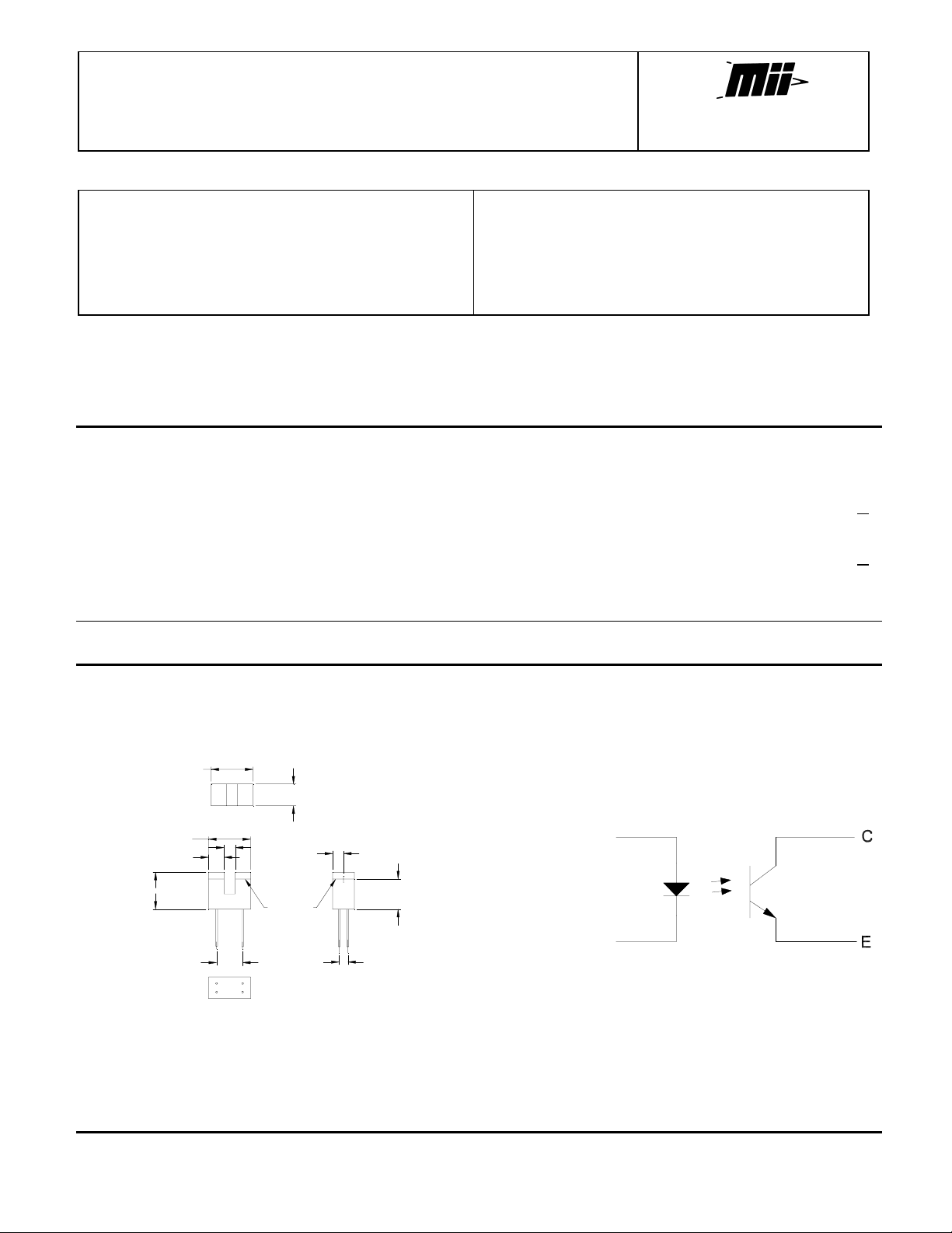
Package Dimensions Schematic Diagram
0.484 [0.48]
0.484 [0.48]
0.177 [0.18]
0.425 [0.43]
0.300 [0.30]
NOTE: ALL LINEAR DIMENSIONS ARE IN INCHES (MILLIMETERS)
MICROPAC INDUSTRIES, INC. OPTOELECTRONIC PRODUCTS DIVISION
_
+
ES
K
A
0.250 [0.25]
0.130 [0.13]
OPTICAL
CENTER
E
C
0.125 [0.13]
0.348 [0.35]
LINE
0.100 [0.10]
www.micropac.com
A
K
725 E.Walnut Str., Garland, TX 75040
••••
E-MAIL: OPTOSALES @ MICROPAC.COM
(972)272-3571
••••
Fax (972)487-6918
••••

67013
OPTICAL/ELECTRICAL CHARACTERISTICS
At 25°C unless otherwise specified.
PARAMETER SYMBOL MIN TYP MAX UNITS TEST CONDITIONS
Input Diode Forward Voltage V
Input Diode Reverse Current I
OUTPUT PHOTOTRANSISTOR
At 25°C unless otherwise specified.
PARAMETER SYMBOL MIN TYP MAX UNITS TEST CONDITIONS
Collector – Emitter Breakdown Voltage V
Emitter – Collector Breakdown Voltage V
Collector – Emitter Dark Current
(BR)CEO
(BR)ECO
I
COUPLED CHARACTERISTICS
At 25°C unless otherwise specified.
PARAMETER SYMBOL MIN TYP MAX UNITS TEST CONDITIONS
Collector – Emitter Saturation Voltage V
Collector Current I
CE(SAT)
C(ON)
R
CEO
SLOTTED OPTICAL INTERRUPTER
F
30 V IC = 1 mA
5VI
4mA
1.7 V IF = 20mA
100 mA VR = 3V
= 100µA
E
100 nA
0.40 V IC = 2 mA, IF = 20mA
VCE = 10V
VCE = 5V,
IF = 20mA
-001 Commercial
-101 with 100% screening
MICROPAC INDUSTRIES, INC. OPTOELECTRONIC PRODUCTS DIVISION
www.micropac.com
E-MAIL: OPTOSALES @ MICROPAC.COM
725 E.Walnut Str., Garland, TX 75040
••••
(972)272-3571
••••
Fax (972)487-6918
••••
 Loading...