

MII 53259 Datasheet

53259
400V / 50Ω HERMETICALLY SEALED
POWER MOSFET OPTOCOUPLER
Mii
MICROCIRCUITS DIVISION
Features:
• Hermetically Sealed 8-Pin Dual-In-Line
package
• Normally Closed Contact
• Performance over –55°C to +125°C Ambient
Temperature Range
• ±400 VDC Blocking Voltage in Bi-directional
Mode
• AC/DC Switching
• Maximum AC / DC Load Current: 0.12 A / 0.24 A
• 1500 VDC Withstand Test Voltage
• Optically Isolated
• 1.5 A Output Surge Current
• Same foot print as HSSR 7111 / Mii 53111
DESCRIPTION
The 53259 is a single channel power MOSFET optocoupler. Low on-resistance of the MOSFET outputs, combined
with 1500 VDC isolation between input and output, makes this optocoupler ideal for many solid state relay
applications. Operation is specified over the full military temperature range. The part is supplied in an eight-pin,
dual-in-line ceramic package, available in variety of quality levels from COTS to class K including any custom
screening requirements. The basic data sheet part is environmentally screened to H level in accordance with Table
C-IX of MIL-PRF-38534. For ordering part number; consult with Micropac factory for detail. The part is normally
shipped with gold plated leads, but lead finishes per MIL-PRF-38534 are available.
Functionally, the device operates as a single-pole, normally closed (1 Form B) solid state relay. The device is
actuated by an input current, which can be supplied from standard logic types such as open-collector TTL. The
input current biases a light emitting diode that is optically coupled to an integrated photovoltaic diode array. The
photovoltaic array powers control circuitry that operates the output MOSFETs.
Optimum switching of either AC or DC loads is provided by a configurable output. For AC loads, connection A in
Figure 1 must be used. Connection A will also switch DC loads but connection B, in Figure 1, provides DC-only
operation with the advantages of substantial reduction in on-resistance and twice the output current capability as
that obtained with connection A.
Applications:
• Satellite / Space Systems
• Military / High Reliability Systems
• Power Distribution Control
• AC/DC Electromechanical or Reed Relay
Replacement
• I/O Modules for Automated Test Equipment
• Process Control
• Telecom Applications
• Medical Electronics
Micropac Industries cannot assume any responsibility for any circuits shown or represent that they are free from patent infringement.
Micropac reserves the right to make changes at any time in order to improve design and to supply the best product possible.
MICROPAC INDUSTRIES, INC.
www.micropac.com
MICROCIRCUITS DIVISION • 905 E. Walnut St., Garland, TX 75040 • (972) 272-3571 • Fax (972) 494-2281
E-MAIL: hybridsales@micropac.com 7/29/02
Pg. 1 of 6
53259 Power MOSFET Optocoupler
___________________________________________________________________________________________
ABSOLUTE MAXIMUM RATINGS
Storage Temperature Range ..................................................................................................................-65°C to +150°C
Operating Ambient Temperature - T
Junction Temperature - T
........................................................................................................................................150°C
J
.....................................................................................................-55°C to +125°C
A
Lead Solder Temperature (1.6mm below seating plane for 10 seconds) ............................................................260°C
Average Input Current - I
Peak Repetitive Input Current - I
Peak Surge Input Current - I
Reverse Input Voltage - V
........................................................................................................................................20 mA
F
(Pulse Width < 100ms; duty cycle < 50%) ..................................................40 mA
Fpk
surge (Pulse Width < 0.2ms; duty cycle < 0.1%) .......................................... 100 mA
FPK
....................................................................................................................................5 V
R
Output Current
Connection A – I
Connection B - I
..........................................................................................................................................0.12 A
O
..........................................................................................................................................0.24 A
O
Inrush Output Current
Connection A - I
surge … ........................................................................................................................... 1.5 A
Opk
Output Blocking Voltage
Connection A - V
Connection B - V
..................................................................................................................................± 400 VDC
O
........................................................................................................................ 0 V to +400 VDC
O
Output Power Dissipation ..............................................................................................................................500 mW
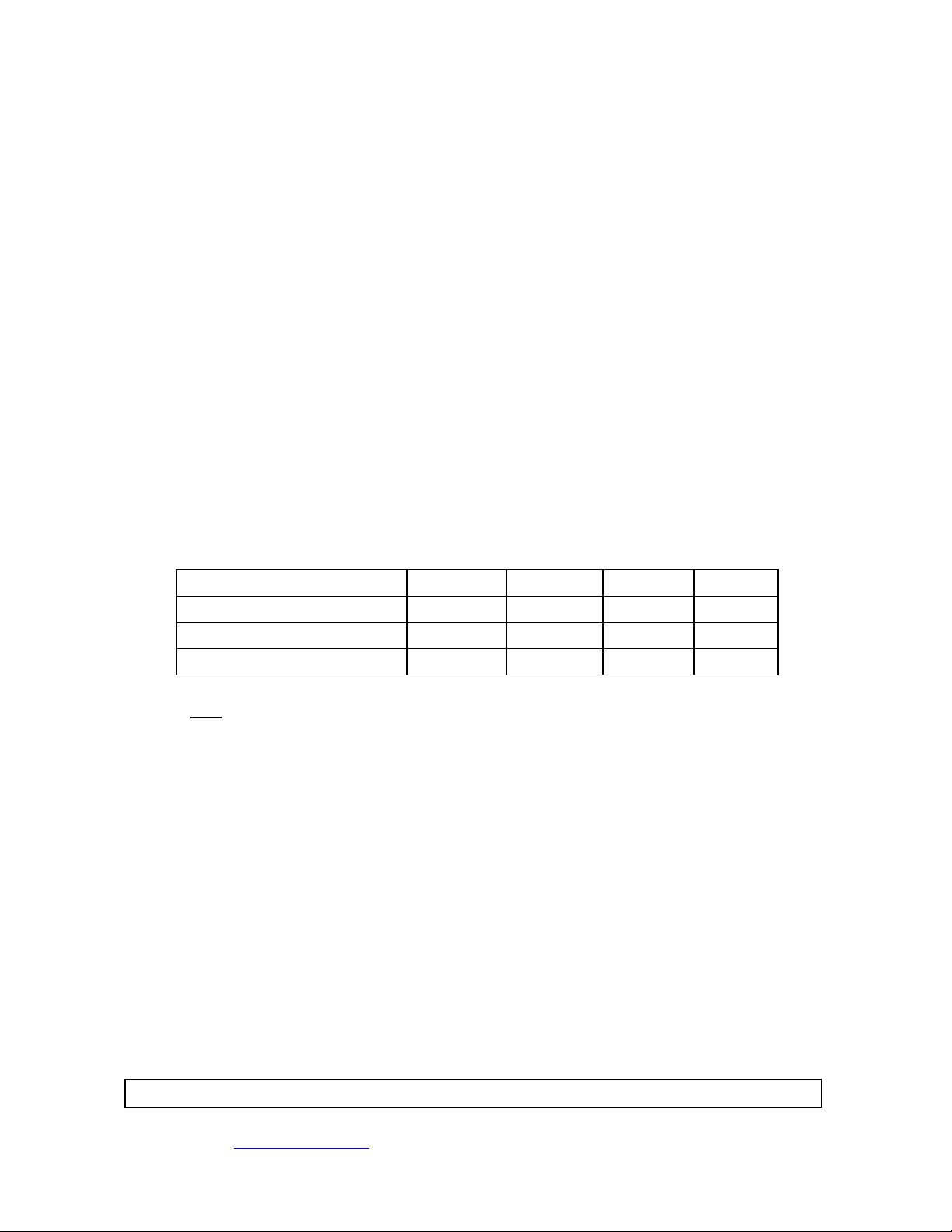
RECOMMENDED OPERATING CONDITIONS:
PARAMETER SYMBOL MIN MAX UNITS
Input Current (off) I
F (OFF)
Input Voltage (on) V
Operating Temperature T
F (ON)
A
5 20 mA
0 0.6 VDC
-55 +125 °C
Note: On state means contact closed. Off state means contact open.
Micropac Industries cannot assume any responsibility for any circuits shown or represent that they are free from patent infringement.
Micropac reserves the right to make changes at any time in order to improve design and to supply the best product possible.
MICROPAC INDUSTRIES, INC.
www.micropac.com
MICROCIRCUITS DIVISION • 905 E. Walnut St., Garland, TX 75040 • (972) 272-3571 • Fax (972) 494-2281
E-MAIL: hybridsales@micropac.com 7/29/02
Pg. 2 of 6
 Loading...