

Midland 91-1060-91-1110, 91-4050-91-4100, P25/FM Service Manual

SERVICE MANUAL ADDENDUM
P25/FM TWO-WAY
LAND MOBILE RADIO
BASE TECH III BASE/REPEATER
STATION
91-1060-91-1110
91-4050-91-4100
LOW CURRENT MODELS
VHF HIGH BAND
UHF BAND
Part Number: 680-100-2049
Revision A
1/12

Important Information
All rights reserved. No part of this publication may be reproduced, transmitted,
transcribed, stored in a retrieval system, or translated into any language without the
written permission of Midland Radio Corporation.
No part of any copyrighted computer programs contained in the products referred to in
this manual may be copied or reproduced without the express written consent of Midland
Radio Corporation.
Midland Radio Corporation reserves the right to change the products described in this
manual without prior notice.
© 2012 Midland Radio Corporation
This manual is designed to facilitate the set-up and service of the Midland 91-1060 / 1110
91-4050 / 91-4100 P25 Base Tech III series. As necessary, service manual supplements
will be published and distributed on the following forms:
Manual Addition (MA) For supplemental information useful in product
service or improvement. Printed on BLUE
paper.
Change Notice (CN) For details about changes made during
production by model and serial number. Printed
on YELLOW paper.
Manual Correction (MC) For correcting literature errors not related to
production changes. Printed on GREEN paper.
Technical Bulletin (TB) For solutions to field problems and tips for
performance improvement. Printed on PINK
paper.
Comments or suggestions concerning areas of manual improvemen t are welcome.
© 2012 Midland Radio Corporation ii

TABLE OF CONTENTS
Manual Supplement Information ii
Table of Contents iii
Acronyms and Abbreviations iv
GENERAL INFORMATION
Specifications 1-2
Accessories 3-4
PREPARATION
Alignment 5-12
CIRCUIT DESCRIPTION
Description 13-18
DIAGRAMS
VHF/ UHF General Block Diagrams 19-22
Front Panel Unit Schematic 23
Analog Logic Unit Schematic 24
VHF RX Main Unit Schematic 25
VHF RX VCO Unit Schematic 26
VHF TX Main Unit Schematic 27
UHF RX Main Unit Schematic 28
UHF RX VCO Unit Schematic 29
UHF TX Main Unit Schematic 30
Front Panel Unit Layout 31
Analog Logic Unit Layout 32
VHF RX Main Unit Layouts 33
VHF RX VCO Unit Layout 33
VHF TX Main Unit Layouts 34
UHF RX Main Unit Layouts 35
UHF RX VCO Unit Layout 35
UHF TX Main Unit Layouts 36
Chassis Exploded View 37
Palm Microphone Schematic 39
PARTS
Low Current Specific Parts List…………….. 40-56
Replacement Parts Ordering 57
iii © 2012 Midland Radio Corporation

ACRONYMS AND ABBREVIATIONS
Below is a list of common electrical abbreviations used in documentation.
CTCSS --------------------- Continuous Tone-Controlled Squelch System
DCS (or CDCSS) --------- Continuous Digital-Controlled Squelch System
EEPROM ------------------ Electrically Erasable Programmable Read Only
Memory
MIL SPEC ------------------ Military Specification
RX --------------------------- Receive
TX --------------------------- Transmit
SINAD ---------------------- The ratio in decibels of signal + noise +
distortion to noise + distortion
VCO ------------------------ Voltage Controlled Oscillator
TCXO ---------------------- Temperature Compensated Crystal Oscillator
PLL ------------------------- Phase Locked Loop
© 2012 Midland Radio Corporation iv

General Information
SPECIFICATIONS -VHF
General
Frequency Range: A Band: 136-156 MHz, B Band: 146-174 MHz
Number of Channels: 500 channels with name, 10 groups of 50 channels
Channel Spacing: FM 12.5 / 20 / 25 / 30 kHz
Digital C4FM
Operation Mode: Simplex / Duplex / Full Duplex/ Repeat
Antenna Impedance: 50 ohm unbalanced
Power Supply: DC 13.6 V, negative ground only
Consumption: <120mA Standby
@RX ~1 A
@TX ≤ 12 A (60W), ≤ 20 A (110W)
Environmental Conditions: -30 to +60 degrees C, 95% humidity @ 35C
Dimensions: 18.2” (w) x 3.4” (h) x 14.2” (d), (462 mm x 88 mm x 360 mm)
Weight: 24 lbs (11 kgs)
Transmitter
Output Power: (91-1060) 25-60 W, continuous
(91-1110) 5-110 W, continuous
Switchable Bandwidth: Full Sub Band
Maximum Deviation: ± 5kHz (wide band), ± 2.5 kHz (narrow band)
Frequency Stability: ≤1.5 ppm std, 10 MHz external optional
Frequency Response: +1 dB / -3 dB, 300-3000 Hz, 1 kHz reference
FM Hum and Noise: ≤ 50 dB @1kHz 70% mod., ≤ 50 dB Digital mode
Modulation Distortion: ≤ 3%
Spurious & Harmonics: ≤ 0.25µW (≥ 80 dBc)
Receiver
Switchable Bandwidth: Full Sub Band
IF Frequencies: 1
Frequency Stability: ≤1.5 ppm
Sensitivity: ≤ 0.40 µV @ 20 dB N.Q., ≤ 0.30 µV @ 12 dB SINAD
≤ 0.30µV, Digital 5% BER
Squelch Sensitivity: ≤ 0.25 µV
Selectivity: ≥ 85 dB @ 25 kHz, ≥ 80 dB @ 12.5 kHz (TIA-603)
≥ 80 dB Digital
Intermodulation: ≥ 85 dB
Spurious Response: ≥ 100 dB
AF Response: +1 / -3 dB, 300-3000 Hz, 1 kHz reference
AF Distortion: ≤ 3% @ 1 kHz 60% mod.
Audio Output Power: 7.5 Watts @ 8 Ώ/ 10 Watts @ 4 Ώ
Signal to Noise Ratio: ≥ 50 dB @ 1 kHz 70% mod. (wideband), ≥ 45 dB (narrowband)
st
IF: 48.4 MHz, 2nd IF: 455 kHz
Low Current Base Tech 3.5
1 © 2012 Midland Radio Corporation

General Information
Low Current Base Tech 3.5
SPECIFICATIONS -UHF
General
Frequency Range: A Band: 400-435 MHz, B Band: 440-475 MHz
C Band: 465-500 MHz, D Band: 485-520 MHz
Number of Channels: 500 channels with name, 10 groups of 50 channels
Channel Spacing: FM 12.5 / 20 / 25 / 30 kHz; Digital C4FM
Operation Mode: Simplex / Duplex / Full Duplex/ Repeat
Antenna Impedance: 50 ohm unbalanced
Power Supply: DC 13.6 V negative ground only
Consumption: <120mA Standby
@RX ~1 A
@TX ≤ 12 A (60W), ≤ 20 A (110W)
Environmental Conditions: -30 to +60 degrees C, 95% humidity @ 35C
Dimensions: 462 mm (w) x 88 mm (h) x 360 mm (d); 18.2” x 3.4” x 14.2”
Weight: 11 kg (24 lbs.)
Transmitter
Output Power: (91-4050) 25-50W continuous
(91-4100) 2-100W continuous
Switchable Bandwidth: Full sub band
Maximum Deviation: ± 5 kHz (wide band); ± 2.5 kHz (narrow band)
Frequency Stability: ≤1.5 ppm std, 10 MHz external optional
Frequency Response: Within +1, -3dB, 300-3000Hz
FM Hum and Noise: ≥ 50 dB @1 kHz 60% mod.; ≥ 50 dB Digital
Modulation Distortion: ≤ 3%
Spurious & Harmonics: ≤ 0.25 µW (-80 dBc)
Receiver
Switchable Bandwidth: Full sub band
IF Frequencies: 1
Frequency Stability: ≤1.5 ppm
Sensitivity: ≤ 0.40 µV for 20 dB N.Q./ ≤ 0.30 µV for 12 dB SINAD
< 0.30 µV Digital 5% BER
Squelch Sensitivity: ≤ 0.25 µV
Selectivity: ≥ 85 dB @ 25 kHz; ≥ 80 dB @ 12.5 kHz (TIA-603);
Intermodulation: ≥ 85 dB
Spurious Response: ≥ 100 dB
AF Response: +1 / -3 dB, 300-3000 Hz, 1 kHz ref.
AF Distortion: ≤ 3% @ 1 kHz 60% mod.
Audio Output (<2% distortion): 7.5 Watts @ 8 Ώ/ 10 Watts @ 4 Ώ
Signal to Noise Ratio: ≥ 50 dB @ 1kHz 60% mod. (45 dB at narrow)
st
IF: 73.35 MHz, 2nd IF: 455 kHz
≥ 80 dB Digital mode
© 2012 Midland Radio Corporation 2

General Information
OPTIONS & ACCESSORIES
71-7220B 30 AMP Rack-mount Power Supply 220/110VAC
71-1230BM Battery Back-up Module for 7220B
71-0033 DC Power Cable, 48”
71-7801 External TX/RX Antenna Relay (Up to 400 Watts)
71-7751 Internal TX/RX Antenna Relay
71-8820D 31-1/2” Indoor Cabinet, complete with locking doors
71-8830D 40-1/4” Indoor Cabinet, complete with locking doors
71-8082 Slide Rails for TX/RX Unit
Low Current Base Tech 3.5
71-8834 Hardware Kit for Cabinets
71-8822-2AS Grounding Kit for 31-½” Cabinets
71-8822-2AT Grounding Kit for 40-1/4” Cabinets
71-8871 12-1/4” Blank Panel
71-8870 10-1/2” Blank Panel
71-8863 3-1/2” Blank Panel
71-8862 1-3/4” Blank Panel
91-1303B USB Programming Cable
91-1480CD Base Tech III Programming Software
71-2020E 16 Channel Tone Remote Termination
71-2022E E&M Expansion Kit used with 71-2020E in
71-8885A/D Option Shelf (only)
71-8885A Option Shelf with Slides / Easy Access & AC Supply
3 © 2012 Midland Radio Corporation
No Battery Charge

General Information
Low Current Base Tech 3.5
71-8885AC Option Shelf with Slides / Easy Access & AC Supply
with Battery Charge
71-8885D Option Shelf with Slides / Easy Access & DC
Operation
71-7206 Tone Termination Lightning / Surge Protection
(2wire / 4-wire)
71-7207 AC Surge Protection Kit (115V only)
71-7655A RF Line Surge Protection
71-8880 90” Aluminum Rack
71-8881 Shipping Hardware Kit, 71-8880
71-8879 Radio Shelf Support Kit (Relay Racks Only)
71-2315 Palm Microphone
71-2316 Desktop Microphone
71-8155-1 VHF Duplexer (3-5MHz Separation) 350W, 150-160
MHz
71-8155-2 VHF Duplexer (3-5 MHz Separation) 350W, 160-174
MHz
71-8152-3 VHF Duplexer (2 MHz Separation) 350W, 150-160
MHz
71-8152-4 VHF Duplexer (2 MHz Separation) 350W, 160-174
MHz
71-8455A UHF Duplexer (3-5 MHz Separation) 350W, 440-
512 MHz
71-8455D UHF Duplexer (3-5 MHz Separation) 350W, 406-
430 MHz
© 2012 Midland Radio Corporation 4

Alignment Procedures
Low Current Base Tech 3.5
THIS PAGE INTENTIONALLY LEFT BLANK
5 © 2012 Midland Radio Corporation

Alignment Procedures
Low Current Base Tech 3.5
RECEIVER (RX MAIN UNIT)
1. Pre-selector and Post-selector Tuning
Both selectors have been pre-tuned at the factory, so no alignment is require d.
2. FVR001 Tight Squelch Level
This potentiometer allows adjustment to the tight squelch level.
3. FVR002 De-mod out Bias Level
This potentiometer allows adjustment to the level of DC Bias on the De-Mod output.
4. L303 VCO Alignment
The VCO has been aligned at the factory to cover full sub-band. However, if you need to re-adjust VCO
after a repair, set the VCO voltage to 10.5 V at the highest end of the sub b and using L303. The VCO
cover must be removed for access.
Note that tuning slug may be glued and breakage could occur.
5. RX 0-dBm Level Adjustment
This is 600 ohm audio available on pins 20 and 21 of the EXT Option port. It is electronically a djuste d.
Ground TP-2 on the Analog Logic Unit PCB, and power-up the radio. See Figure 3 on page 6. The
station is now in Adjust Mode. Release TP-2 from ground. The di splay should look as follows:
RXNS <Adjust>
TXN RX 0dbm Out
C0001 27 / 31 AA
Use the “A” and “B” keys on the front panel to adjust the level up or down. Pressing the “#” key will
change the mode you are adjusting. The “A” key will increase the level while the “B” key will decrease
the level. You will be able to monitor the output if the station is recei v ing a valid carrier and signaling.
Cycle power to the radio to return to normal operation.
NOTE: The other ADJUST Modes are in order of appearance:
RX 0 dbm
REPEA T DE VI
DIGITAL DEVI
ANALOG DEVI
TONE DEVI
CTC DEVI WID
CTC DEVI NRW
© 2012 Midland Radio Corporation 6

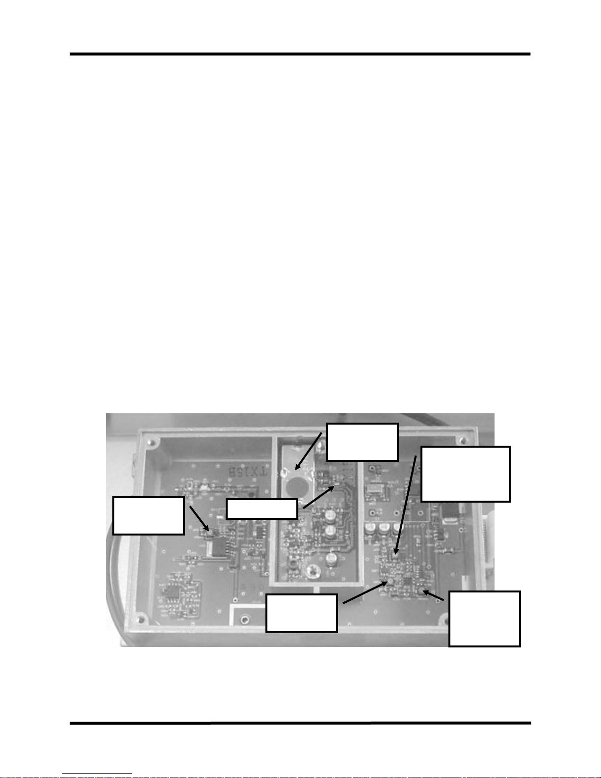
FVR002
De-mod Bias
FVR001
Tight Squelch
Alignment Procedures
Low Current Base Tech 3.5
Figure 1: Receive Module (RX Main Unit) Alignment Adjustment s
7 © 2012 Midland Radio Corporation
Alignment Procedures
Low Current Base Tech 3.5
EXCITER (TX MAIN UNIT)
1) FVR201 Sub-Audible Modu lation Balance
This potentiometer sets modulation balance below 300 Hz. Carefully align this potentiometer to obt ain
flat deviation from the lowest to the highest frequency programmed in the transmitter.
2) FVR202 Sub-Audible Modu lation Deviation
This potentiometer determines low frequency (below 300Hz) deviation. When POCSAG an d DCS are
used, it may be necessary to readjust to have enough deviation and fidelity at lower frequencies.
FVR201 and FVR202 are used together to adjust amplitude and fidelity of square wave output of the
transmitter in Analog Mode.
3) FVR203 Carrier Frequency Trim
This potentiometer adjusts carrier frequency. Its range will allow for +/- 200 Hz adjustment from the
desired (programmed) frequency.
4) FVR204 Exciter Output Power
This potentiometer adjusts the exciter’s output power level. This is nominally 80 mW.
5) L303 VCO Alignment
The VCO has already been aligned at the factory. However, if you need to re-adjust VCO af ter a rep air,
set the VCO voltage to 10.5 V at TP301 at the highest end of the sub band using L303.. This p art can be
found beneath the cover. See Figure 2. Note that tuning slug may be glued and breakage could
occur.
VCO L303
FVR204
Output Power
(under cover)
TP301)
FVR203
Frequency Trim
FVR201
Sub-Audible
Balance
FVR202
Sub-Audible
Deviation
Figure 2: Exciter Module (TX Main Unit) Alignment Adjustments
© 2012 Midland Radio Corporation 8
6) Electronic Transmitter Alignment
A
The station must first be put into “Adjust Mode.”
Figure 3: Entering Alignment Adjust Mode
7)
Entering & Exiting Alignment Adjustment Mode
a) If not already, power off the radio.
Alignment Procedures
Low Current Base Tech 3.5
TP2
lignment Mode
b) Terminate the radio TX port into a 50 ohm load rated for at least 150 Watts.
c) Place the Local / Remote Switch (on the front panel of the 71-8885 Deluxe Option Housing if
equipped) into the Local position.
d) Ground TP2 on the Analog Logic Unit PCB (the nearby PA Unit chassis is a good ground point.)
e) Apply power to the radio. The radio should power-on directly into the Adjust mode (indicated by
“<Adjust>” displayed on-screen.) If the radio displays an error message on the fourth line of the
LCD, check that the Local / Remote Switch is in the Local position.
f) Open the ground connection to TP2.
g) When the desired alignment procedures have been conducted, remove powe r from the radio to exit
the adjustment mode. Changes made during alignment will be a utomatically stored when e ntered.
h) The following adjustment are available in order of appearance:
RX 0 dbm
REPEA T DE VI
DIGITAL DEVI
ANALOG DEVI
TONE DEVI
CTC DEVI WID
CTC DEVI NRW
9 © 2012 Midland Radio Corporation

Alignment Procedures
Low Current Base Tech 3.5
8) Maximum Analog Deviation Limiting Alignment (Base Station and Repeater)
a) Press the “#” key on the Front Panel until second line of the LCD displays “ANALOG DEVI.”
b) Apply a 1 kHz tone at the microphone input at a level required to obtain 60% system deviation. Use
pins 1 and 2 (pin 2 = ground).
c) Activate PTT by grounding pin 4 of the microphone jack. Note the audio generator level setting.
d) Increase the audio level by 20 dB (equivalent to 10x voltage increase).
e) Press the “A” key to increa se or the “B” key to decrease the system deviation until it is just below
±4.5 kHz without CTCSS modulation or ±4.7 kHz with CTCSS modulation (25 / 30 kHz channel
spacing) or ±2.3 kHz without CTCSS modulation or ±2.5 kHz with CTCSS modulation (12.5 / 15
kHz channel spacing). The radio is in limiting at this point, so distortion will be higher according to
the service monitor. Deviation should be measured with at least a 50 Hz to 15 kHz filter enabled (no
higher than 20 kHz).
f) Deactivate the transmitter.
9) Analog Repeater Deviation Alignment (This should be checked AFTE R St ep 8 has been accomplished)
a) Press the “#” key on the Front Panel until second line of the LCD displays “REPEAT DEVI.”
b) Set the radio to a channel programmed for repeat mode (wide or narrow band).
c) Inject a -47 dBm ± 3 dB RF signal modulated with a 1 kHz tone into the receiver input at 60%
system deviation. Enable sub-audible signaling if the radio (repeater) is configured as so.
d) At this time, the radio (repeater) should be transmitting.
e) Measure the transmitter deviation level. Enable audio filtering of 300 Hz to 3 kHz if sub-audio
signaling is present. If sub-audio signaling can not be filtered, set the radio to a channel
programmed without sub-audio signaling enabled, and disable sub-audible signaling on the signal
source.
f) Press the “A” key to increase or the “B” key to decrease the repeater transmitter deviation until it is
60% ± 5% system deviation.
g) Remove the RF signal.
10) Analog CWID/DTMF Deviation Alignment
a) To best perform this alignment, it is preferred to program a radio channel to the desired operational
parameters intended for daily operation. It is typical that this channel is to also transmit the normal
CWID tone sequence. If no channel has been programmed as described, continue with the
remaining steps.
b) Press the “#” key on the Front Panel until second line of the LCD displays “TONE DEVI.”
c) Activate PTT.
d) Press the “A” key to increa se or the “B” key to decrease the CWID transmitter deviation until it is
40% ± 5% system deviation.
e) Deactivate PTT.
© 2012 Midland Radio Corporation 10

Alignment Procedures
Low Current Base Tech 3.5
11) CTCSS Deviation Alignment
a) Press the “#” key on the Front Panel unti l the second line of the LCD displays “CTC DEVI WID.”
b) Activate PTT.
c) While monitoring peak FM deviation, adjust the deviation level to obtain 500 Hz ± 10 Hz positive
and negative peak deviation. Enable audio filtering below 300 Hz only. Press the “A” key to
increase or the “B” key to decrease the transmitter wideband CTCSS deviation level.
d) Deactivate PTT.
e) . Press the “#” key on the Front Panel until the second line of the LCD displays “CTC DEVI NRW.
f) Activate PTT.
g) While monitoring peak FM deviation, adjust the deviation level to obtain 250 Hz ± 10 Hz positive
and negative peak deviation. Enable audio filtering below 300 Hz only . Press the “A” key to increase
or the “B” key to decrease the transmitter narrowband CTCSS deviation level.
h) Deactivate PTT.
12) C4FM Digital Deviation Alignment
a) Press the “#” key on the Front Panel unti l the second line of the LCD displays “DIGITAL DEVI.”
b) Activate PTT.
c) While monitoring peak FM deviation, adjust the deviation level to obtain 2827 Hz ± 283 Hz positive
and negative peak deviation. Press the “A” key to increase or the “B” key to decrease the
transmitter C4FM digital deviation level.
d) Deactivate PTT.
e) Exit alignment mode by cycling power to the radio.
f) After radio reset is complete, press the Shift key followed by the numbe r 0 key.
g) Press the number 2 key to transmit the Standard Transmitter Sym bol Rate Pattern.
h) Activate PTT.
i) Monitor peak FM deviation. Verify that both positive and negative peak deviation levels each fall
within 2544 Hz to 3111 Hz deviation.
j) Press the number 3 key to transmit the Standard Transmitter Low Deviation Pattern.
k) Monitor peak FM deviation. V erify that both positive and negative peak deviation levels each fall
within 848 Hz to 1037 Hz deviation.
l) Deactivate PTT.
11 © 2012 Midland Radio Corporation
Alignment Procedures
A
A
Low Current Base Tech 3.5
FRONT PANEL UNIT
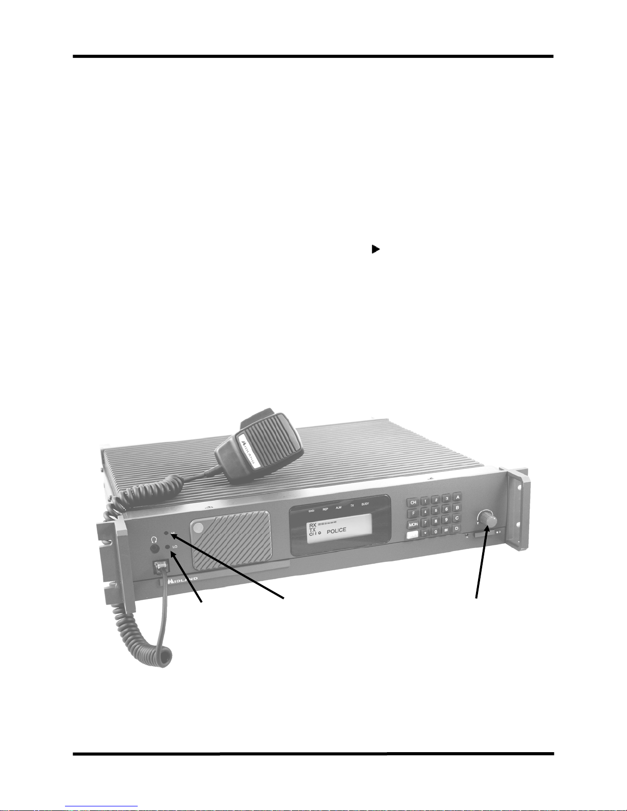
1) VR40
2) F
1 Alignment
This is to set volume level by pulse code switch. Press on
Press again, and the backlight lighting level can be se
Press a third time, and the backlight timer ca
n be set.
t.
VR401 Transmitter Hi-Power Alignment
ce and Noise Squelch can be set.
This potentiometer allows for fine adjustment of the High-Power level of the transmitter output whe n
the radio is set to High-Power Mode. S tation will indicate
in the right side of the display when in
High-Power Mode. Press “SHIFT,” then “2” to toggle transmitter Power Mode.
Note: “TX Power Change” MUST be enabled in software programming to toggle TX Power
from the Front Panel.
3) FVR402 Transmitter Low-Power Alignment
This potentiometer allows for fine adjustment of the Low-Power level of the transmitter output when
the radio is set to Low-Power Mode. The station must be on a low-power channel, or the station
must be placed in the Low-Power Mode. Press “SHIFT,” then “2” to toggle transmitter Power Mode.
© 2012 Midland Radio Corporation 12
FVR402
Low-Power Level
djustment
FVR401
High-Power Level
djustment
VR401
itchPulse Code Sw
Function by # of presses:
1. Volume
2. Noise Squelch
3. Backlight Dim
4. Backlight Timer

Circuit Description
Low Current Base Tech 3.5
LOW CURRENT IMPROVEMENTS
In order to improve standby current consumption the Receiver Unit, Transmitter Unit, Analog Logic Unit and
Front Panel Unit have been modified from the original Base Tech III configuration. These improvements will
start to be incorporated into all Base Tech III radios manufactured in 2012. Earlier versions of Receiver Unit,
Transmitter Unit and Analog Logic boards should not be mixed. RF Power Amplifiers remain unchanged. A
label marked “Low Current Variant” will be affixed to all receiver, transmitter, analog logic and front panel
units for easy identification. The Front Panel Unit may be used with either standard or Low Current models.
RECEIVER UNIT
1) RF Section
An incoming signal is fed to the pre-selector bandpass filter and amplified by Q861. It is then fed to the
post-selector bandpass filter. The balanced mixer, consisting of IC811, produces the first IF (VHF =
48.5 MHz/ UHF = 73.35 MHz) by injection from the 1
2) IF Section
The first IF signal is fed to crystal filter, XF801, then amplified by Q810. Again, this signal is fed to the
4-pole crystal filters and amplified by Q001. Following amplification, the signal is fed to the 2
processor (IC001). The 2
signal (455 kHz). IC001 amplifies the 2
nd
local oscillator (crystal) signal is directed to IC001 to produce the 2nd local IF
nd
local IF signal, which then becomes an audio baseband signal
st
local oscillator generated by RX VCO.
nd
IF
through a detector circuit internal to IC001. This audio signal is then directed to the low pass filter
inclusive within IC002, after which it is sent to audio processor, IC3.
3) VCO section
The oscillator circuit produces the 1
st
local oscillator signal
(VHF = RX frequency + 48.5 MHz / UHF = RX frequency – 73.35MHz).
st
The 1
local oscillator signal is amplified by buffer Q302, then amplified by pre-amplifier IC301 and
post-amplifier Q303. The amplified signal is fed to the first balanced mixer. The VCC for the VCO has
been changed from 7 volt s to 5 volts.
4) PLL Section
The PLL IC, IC806, with integrated pre-scaler compares the phase between the VCO frequency and
reference oscillator frequency (12.00 MHz) by method of dividing the frequency, and produces VCO
control signal. Then, this control signal is fed to the charge pump and fed to the low-pass-filter. The
supply voltage of charge pump is multiplied by IC807 (to approx. 13 V) to achieve greater S/N ratio.
5) Low Current Improvements
An additional 5.5 volt dc source has replaced the 12 V dc source for main on board power. An additional
12 volt line has been added for the 7 V dc regulator. This significantly reduces current consumption
losses to heat.
13 © 2012 Midland Radio Corporation

Circuit Description
Low Current Base Tech 3.5
EXCITER UNIT
1) VCO Section
The oscillator circuit generates transmitter frequency. Then this signal is fed to the 3-stage of amplifier,
buffer amplifier Q302, pre-amplifier IC301 and post amplifier Q303 and lead to the final amplifier, and
lead to the final amplifier.
2) PLL section
Basically, the circuit description is the same as RX. The PLL IC inclusive with prescaler (IC208)
compares the phase between VCO signal and reference oscillator frequency (12.00 MHz) by method of
dividing the frequency, and produces VCO control signal. Then this VCO control signal is fed to the
charge pump, and fed to the low-pass-filter. The supply voltage of charge pump is amplified by IC210
(to approx. 13 V) to achieve greater S/N ratio.
3) Modulation Section
The modulation signal is fed to both VCO and the reference oscillator (TCVXO 12.00 MHz), this permits
very flat modulation characteristics against low frequency (DC). This is an advantage when BASE
TECH III is used as a POCSAG transmitter.
4) TX Exciter Section
The VCO signal is amplified by Q211 to achieve 80 mW.
5) Low Current Improvements
An additional 5.5 volt dc source has replaced the 12 V dc source for main on board power. An additional
12 volt line has been added for the 7 V dc regulator. This significantly reduces current consumption
losses to heat.
POWER AMPLIFIER
1) Power Amplifier (VHF = 5-110W/ UHF = 2-100W)
The 80 mW signal from TX Exciter stage is fed to PM501 to produce 10W output. Then, Q504 and Q505
amplify to 110/100W. This signal is fed to the Low-Pass- Filter to eliminate the harmonics and spurious
frequencies. An APC circuit formed by IC502 stabilizes the output power at the set level. An IC501
protects final stage transistors from the reverse power caused by a mismatched antenna system
2) Power Amplifier (VHF = 60W / UHF = 50W)
The 80 mW signal is fed to PM501 to achieve 60/50W output power. Then, signal is fed to the LPF to
eliminate the harmonics spurious frequencies. An APC circuit formed by IC502, IC503, Q504 and
Q505 stabilizes the output power at the set level. IC501 protects PM501 from the reverse power
caused by a mismatched antenna system
© 2012 Midland Radio Corporation 14

Circuit Description
Low Current Base Tech 3.5
DESCRIPTION OF CIRCUITS TO STABILIZE TX AND RX FREQUENCY
The transmitter and receiver each use a TCVXO (Temperature Compensated Voltage-Controlled Crystal
Oscillator) to generate the 12.00 MHz reference frequency used within their respective PLL and VCO
circuits. The accuracy of the TCVXO is better than +/- 0.00015% over the range of –30 degree C to +60
degree C.
DESCRIPTION OF CIRCUIT TO SUPPRESS SPURIOUS EMMISSIONS AND MODULATION LIMITING
A multiple pole Low Pass Filter is used after the final power amplifier stage. It is designed to sharply
attenuate spurious and harmonics frequencies above the highest frequency in the sub-band of the radio.
Modulation limiting is performed by TX audio processor, CMX7041L4, located on the Analog Logic Unit.
Internal limiting/compression amplifier provides excellent limiting with minimum distortion.
In addition to modulation limiting, this device contains all circuitry to perform pre-emphasis, band pass
shaping and CTCSS/ DCS encoder.
ANALOG LOGIC UNIT
1) Microcomputer (CPU) Section
CPU IC1, H8S2239 is the 16-bit processor contained 320kb flash memory 6k RAM inside. The CPU
controls all functions of Base Tech III. A flash memory permits on-board-up-grade when new firmware
is released.
2) EEROM Section
IC6 is the 64k bit EEROM. This memory contains all the channel data
3) Audio Processor Section
IC2 is for TX and IC3 is for RX audio processors. CTCSS and DCS are processed within these audio
processors. In previous releases the CTCSS and DCS were processed within separate processors.
This also improves current consumption and simplifies the sub-signaling routines.
4) Low Current Improvements
A DC-DC converter (IC 43) has been added to replace the analog 12 volt to 5 volt regulator (IC5).
The DC to Dc converter runs at 170kHz and directly regulates 5.5 volts with no losses to heat
dissipation. This significantly reduces overall current consumption.
DIGITAL LOGIC UNIT (DSP)
IC1 acts as the DSP control for both incoming digital signal converting it to analog and analog
signal to C4FM digital signal. External flash memory within IC2, has 4Mb capacity, contains all
data. Program data is stored in 256 k-bytes of memory integrated within IC1.
15 © 2012 Midland Radio Corporation
 Loading...