

Page 1

CAD-POCSAG
PC BASED POCSAG ENCODER (Serial DB9 Version)
CAD-POCSAGU
PC BASED POCSAG ENCODER (USB Version)
Manual Revision: 2012-05-09
Covers Firmware Revisions:
CA
D-POCSAG: 1.0
Covers Software Revisions:
CAD-POCSAG: 2.5 & Higher
Covers Hardware Revisions:
CAD: 219F & Higher
Page 2

SPECIFICATIONS
Operating Voltage 10-15 VDC
Operating Current 22 mA
NRZ Data Rate 512, 1200, & 2400
PTT Output Current 1 A
Data Output Level 0-1/2 VIN
Data Output Impedance 5 K Ohm
Dimensions 5.87 x 4 x 1.5”
Operating Temperature -30° to +60° C
Maximum Message Length 100 characters
SYSTEM REQUIREMENTS
Windows 98 Second Edition or Higher
Pentium 1 or Higher
10 MB of Disk Space
64 MB of RAM
Operating System: Windows 98 SE, 2000, XP SP2 and higher
Processor: Pentium 1 or Higher
Hard-Drive Space: Minimum 10 MB
RAM: Minimum 64 MB
Serial DB9 Version is ordered as CAD-POCSAG.
USB Version is ordered as CAD-POCSAGU.
GENERAL INFORMATION
Midian Electronics’ CAD-POCSAG enables the user to encode POCSAG pages to single or multiple pagers at
one of three baud rates (512, 1200 or 2400). Files inserted into a network folder can also be encoded by the
CAD-POCSAG.
POCSAG: POCSAG is a digital paging format used for alpha and numeric pages. POCSAG was originally
specified by the British Ministry of Posts and Telecommunications.
Page 3
HARDWARE INSTALLATION
Pin 1 – Ground – Connect to ground in the base station.
Pin 2 – B+ - Connect to a 10-15 VDC source in the base station.
Pin 3 – PTT Output – Connect to the PTT input of the radio. This open collector provides a ground during PTT.
Pin 5 – Data Output – Connect to the Data Input of the radio which provides a flat frequency response.
Pin 9 – COR Input – Connect to a point in the Squelch or CTCSS circuit that changes logic level when carrier is
received. A radio whose squelch circuit provides a logic low or logic high can readily turn the COR transistor on
and off. If the point that this lead is hooked to only makes a minute change in voltage, it will be necessary to
adjust the values of the input resistors to cause the COR transistor to change states.
The USB connector is P3.
The following are the pins used on the Female DB-9 connector P2 (RS-232).
P2-2 – TX Output
P2-3 – RX Input
P2-4 – Data Terminal Ready
P2-5 – Ground
P2-6 – Data Set Ready
P2-7 – Clear To Send
P2-8 – Request To Send
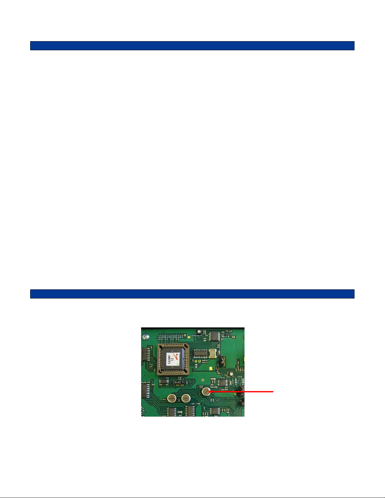
HARDWARE ALIGNMENT
Output Level: To set the output level, command the CAD-POCSAG to send a lengthy page by typing a long
message and sending to multiple pagers. Set R78 for a deviation of ±4.5 kHz at the transmitter.
R78: Output Level
Page 4

SOFTWARE INSTALLATION
Insert the CD-ROM that came with your product, which is labeled “Programming Software & Product Manual CDROM” into your CD drive. The CD-ROM should launch automatically. If it does not, simply navigate to the drive
letter of your CD-ROM and double-click ‘Browser.exe’. This will launch the web browser and display the home
page so that you may view the contents of the Programming Software & Product Manual CD-ROM.
1. From the main page click the link of the navigation bar titled Misc. Software.
2. After the new page appears click on the link in the main window labeled CAD Series Software.
3. This will open a page that lists all of our CAD products. Double-click on the link titled CAD-POCSAG (Page
Master) > this will automatically start the installation program.
4. Follow the installation instructions.
Page 5

Modem Parameters:
PRODUCT PROGRAMMING
Baud Rate: Select the baud rate of the POCSAG pagers, either 512, 1200 or 2400 bps.
COR Polarity: This should match the active COR polarity of the radio.
Data Polarity: This polarity is dependent upon the radio and can only be determined by experimentation.
Key-Up Delay: This sets the delay from when the radio starts to transmit until the CAD-POCSAG encodes the
POCSAG sequence.
COR Delay: This sets the time that the channel must be inactive before the unit will attempt to send a page.
Transmit Hold Up: This is a length of time after the POCSAG has been encoded that the transmitter will remain
keyed.
Force Alpha/Numeric Translation: Check this box if the pagers are not capable of 7-bit and 4-bit decoding. If
checked the unit will send each message as 7-bit encoding. If unchecked it will send numeric messages as 4-bit
encoding.
Page 6

Transmit Parameters:
Message Folder Path: The unit can automatically encode files that are deposited into this folder. The files must
use a “.msg” extension and have the cap code on the first line, the client name on the second line and the
message to be sent on the third line. For example:
12345678
John Smith
Call Debbie at 555-1234
Delay Between Message Transmits: This is the amount of time the unit will unkey the transmitter before
attempting to send the next message.
Adding A New Client: Go to Config > Add A New Client. Enter the name of the Client and the cap code of the
pager.
Edit Selected Client: Go to Config > Edit Selected Client. Modify the name and/or the cap code of the client.
Delete Selected Client: Go to Config > Delete Selected Client. This will delete the highlighted client. Right
clicking the highlighted client also enables deleting of the client.
For more detailed instructions on how to use this product, please see the online help files after installing the
product. These may be viewed by launching the CAD-POCSAG (Page Master) and going to Help > Contents.
If you allow your mouse to hover over a data field or the label of a data field, you will see additional details and/or
tips for that section. Pressing the F1 key in a data field will bring up additional help information. More detailed
information is available in the online help files.
Page 7

OPERATION
Sending A Message: To send a POCSAG page select the client or clients to send the message to. Select a
range of clients by selecting the first, holding the shift key, and selecting the last in the range. Multiple clients can
also be selected by clicking on multiple clients while holding the control key. Once the client(s) are selected type
the message and select the send button.
Clearing A Message: To clear a message click on the clear button. This will clear the message field and deselect
the client(s).
Page 8

TECHNICAL NOTES
Radio Compatibility: Midian has taken the utmost care to ensure the CAD integrates with the radio with minimal
impact to the features of the radio. However, some features may not be available in the radio when a CAD is
used. If a feature is not available, please contact Midian to see if the feature can be added.
International Windows Versions: Even though Midian has worked to make this product internationally
compliant, Midian recognizes that there may be additional issues to be resolved.
MIDIAN CONTACT INFORMATION
MIDIAN ELECTRONICS, INC.
2030 N. Forbes Blvd. #101
Tucson, Arizona 85745 USA
Toll-Free: 1-800-MIDIANS
Main: 520-884-7981
E-mail: sales@midians.com
Web: www.midians.com
Page 9

1
2
3
4
5
6
13
12
U9
*
C19
*
10
R2
1M
R22
VSS
-
U3:4
+
LMV324
R14
10K
*
C13
*
6
5
*
R24
18
CKD
RX_S
TX_DIN
TX_OUT
R13
CD
C4
100p
100K
C16
*
R37
*
*
14
U6:2
C61
*
12
13
15
5
4
3
7
8
11
TP1
TOUCH TONE
CAD 100
C5
*
R33
*
R5
*
5
+
U4:2
6
-
*
+5v
4
15
16
Q3
R25
*
VDD
B
R
Q03CLK
*
*C24
JU1C
C101
*
6
C31
4
*
C6
.01u
Q1
13
12
*
7
2
C25
+5v
TP4
EN
Q2
U7:1
*
R6*R7
*
C7
.1u
D1:2
*
R91
*
C14
*
2
5
1
1
-
U5:4
+
*
1
P0.5P0.5
6
P0.2P0.2
7
P0.4P0.4
5
XTALoutXTALout
C2-
FB
*
TP8
C72
*
C71
*
R56
4.7K
VAN
C56
.47u
C41
100p
14
13
7
8
4
5
R57
10K
Q2
B25
*
6
5
C73
+VIN
C50
1u
-
+
U3:2
C80
.001u
LMV324
C60
.47u
R92
0R
R94
0R
10K
R78
R95
*
7
C74
*
C64
.47u
R96
0R
R79
10K
OUTPUT LEVEL
ADJUST
VAN
R82B
330R
R82A
330R
SERIAL OPTION
C75
*
9
-
U3:3
10
+
VAN
C63
R89
*
USB OPTION
C43
560p
R80
10K
LMV324
*
R90
*
5
GND
8
C36
34
T2
*
2
PAD9
PS
16
*
3
2
C69
560p
C44
*
JU8
+VIN
64
-
U13
+
*
C47
OPTION TXOPTION TX
BALANCED
OUTPUT
Q3
BSS
D3:2
CAD POCSAG TONE OUTPUT
SQUELCH OUTPUTSQUELCH OUTPUT
TP3
TX AUDIO OUTPUTTX AUDIO OUTPUT
R81
27K
JU4
*
C45
*
JU9
*
C76
*
5
R97
*
*
11
22
JU5
A6
TZ2
P0300
1 3
*
D3:1
2 3
A6
P1:5
P1:6
C46
1u
P1:7
P1:8ALARM
P1:3
PTT OUTPUTPTT OUTPUT
C70
560p
P1:4
P2:6
4.7KR44
P2:4
4.7KR43
P2:2
P2:3
P2:8
P2:7
P2:5
P2:1
P2:9
P2:10
P3:1
P3:2
P3:3
P3:4
R99
P3:5
*
P3:6
P1:2
+VIN +12-15VDC+VIN +12-15VDC
P1:1
GROUNDGROUND
DSRDSR
DTRDTR
TXOTXO
RXIRXI
RTSRTS
CTSCTS
GNDGND
NCNC
NCNC
NCNC
VCC
D-
D+
GND
NC
4
Q1
3
R59
10K
R61
10K
R63
10K
R65
10K
R67
10K
R69
10K
R71
10K
R73
20K
1
2
3
4
Q0
15
CLR
TP2
U12
CS
SCLK
SI
SO
93LC46B
TP7
R51
*
D4:2
VCC
NC1
NC2
GND
R31
C23
C
4
11
A
42
OSC2
U1
68705FN
44
C8
22p
VDD
R83
10K
TCAP
+5v +5v
+5v
R49
10K
C9
22p
11
R85
10K
12
41
6
8
7
9
2
3.579545 MHz.
43
OSC1
A6
A4
A5
A3
A1
A0
TCAP
IRQ
R55
4.7M
Y1
*
+5v
Q1
BSS
*
R100
10K
R41
100K
+5v
VCCVCC
U5:5
GNDGND
R12
10K
39
D7
R102
*
40
NC3
+5v
27
C4
30
C1
25
C6
38
TCMP
5
A7
23
NC2
3
NC4
22
GND
+5v
4
11
4
VCCVCC
U4:5
*
GNDGND
11
C53
1u
R32
7.5K
*
*
11
12
13
14
+5v
C10
C37
.01u
.1u
37
4
SS
10
A2
VPP
R58
20K
21
B7
R60
20K
20
B6
R62
20K
19
B5
18
NC1
TDO
RDI
SCK
MOSI
MISO
RES
R34
10K
B4
B3
B2
B1
B0
C0
C2
C7
C5
C3
3
2
+
U3:1
-
17
16
15
14
13
31
29
33
32
24
26
28
36
35
34
R54
47K
1
+5V
LMV324
R101
*
R77
4.7K
R48
4.7K
R50
10K
1
R64
20K
R66
20K
R68
20K
R70
20K
R72
20K
+5V
TP6
C52
1u
R53
47K
VAN
C66
*
C67
*
3
2
7
D1:1
2 3
1 3
R17
*
+5v
R36
+5v+5v
U6:1
19
16
R9
*
*
18
R8
*
4
1
3
+
U4:1
2
-
R38
*
+5v
*
3
3
7 14
4
11
2
14
-
1
U5:1
3
+
*
U16
*
VAN
VddVdd
P0.3P0.3
VssVss
XTALinXTALin
Y5
*
+5v
U6:4
*
13
12
8
TP5
2
4
3
C102
*
N/C
JP1:1JP1:2JP1:3JP1:4JP1:5
R26
*
GS
IN-
NC1
St/GT
NC2
ESt
VREF
IN+
*
+5v
GND
R52
*
Y3
*
8
OSC1
U2
*
INH5GND
R15
*
10
1
*
*C68
*C21
*
C22
61614
U8
74HC4046
12
R27
*
U7:2
*
11
R7VSS8EN10Q3
+5v +5v
C104
*
D5
C103
*
9
OSC2
VCC
TOE
STD
PWDN
6
587
R28
JU12_11
11
*
JU10
*
+5v
20
11
12
Q1
13
Q2
14
Q3
15
Q4
17
JU2
*
JU3
*
2
R30
9
*
R29
*
Q0
Q1
Q2
CLK
9
33
22
R40
47K
R39
2.7K
+5v
VCCVCC
U3:5
LMV324
GNDGND
+VIN
C38
.01u
1
1 3
CK
R74
100K
B25
5
U14:2
Q2
*
6
Q3
Y4
C26
*
*
3
OUT3OUT
V+4V+
4
C27
*
GND2GND
EN1EN
1
C30
2
*
*
5
3
6
8
10
7
K1
11
+5V
+5V
R46
100K
PAD3
1
NC12NC
27
NC
9
DSR#
10
DCD#
11
CTS#
NC14NC22NC
PAD5
PAD6
+5V +VIN
C40
.01u
Q4
2 3
8
7
6
5
R86
R87
R88
12
D4:1
22
JU14
+5V
C39
.01u
1
R84
100K
C62
.01u
*
*
*
11
12
13
14
16
2
1
7
2
8
3
9
4
10
13
5
11
14
6
12
15
11
12
10
R47
13
TXD
0R
PAD4
5
RXD
C48
1u
PAD1
NC2NC
3
9
1
3
PAD2
15
D+
U15
*
GND7GND21TEST
GND
18
23
PAD7
5
OUT
C54
1u
Q0
Q1
Q2
CLR
Q3
GND
CK
V+
EN
EN
MF OPTION
R98
0R
+5V
C35
.1u
T1_IN
R1_OUT
T2_IN
R2_OUT
C1+
C1-
6
16
D-
RI#
VCC
VCCIO
3V3V
GND
26
25
VR1
4
5206
IN1
RES
ENA
GND
2
B
16
VCC
MX232
R93
*
NC
NC
NC
NC
1
3
U14:1
*
7
8
9
10
C49
1u
U11
15
28
8
20
4
17
19
24
R75
100K
R76
240K
C42
.001u
2
T1_OUT
V+
T2_OUT
V-6GND
C51
1u
C55
.01u
R1_IN
R2_IN
C2+
C1
T1
C2
C15
*
22
R11
C65
*
.022u
34
5
2
*
PS
16
*
12
13
RC INPUTRC INPUT
P1:12
RC BALANCED INRC BALANCED IN
P1:11
A A
TZ1
P0300
P1:10
RX BALANCED INRX BALANCED IN
11
JU1
PAD8
R10
*
*C18
B B
R18
*
C17
*
R19
*
VAN
C
6
5
Q301
*
-
U5:2
+
R20
*
*
R1
220K
R42B
330R
C3
.01u
R42A
330R
VAN
R3
100K
CAD 200 5 TONE
R16
-
U5:3
+
R21
*
*
14
*
8
R23
10
C20
*
+
U4:4
-
*
9
7
10
VAN
8
9
*
U6:3
CAD 300 ZAP FORMAT
CAD 400 GSTAR FORMAT
A
R35
*
JU13
*
JU1B
*C28
JU7
*
Y2
*
C33 *
*
C C
C32
*
JU6
+5v
*
OPTION
CAD
500/600
FFSK
P1:9
COR INCOR IN
D D
C29
*
+5v
C34B
*
14
17
16
19
C34A
*
2
1
6
9
+5v
20
*
XTL
XTL
RX_IN
4800
TX_ENA
1200
CDRC
VBIAS
DOCUMENT NAME
10
+
8
U4:3
9
-
*
1
2
3
4
MIDIAN ELECTRONICS, INC.
1995-12-30 DML
DATE:
DESIGN:
CJS
DWN BY:
REV:
2012-09-05
5
APPR
CAD-POCSAG
SCHEMATIC
COPYRIGHT ©
2012
REV
H-2
SHEET
1 of 1
6
CP
PROJECT NUMBER
7219
Page 10

- This page intentionally left blank -
Page 11

Page 12

Page 13

1
2
3
4
5
6
13
12
U9
*
C19
*
10
R2
1M
R22
VSS
-
U3:4
+
LMV324
R14
10K
*
C13
*
6
5
*
R24
18
CKD
RX_S
TX_DIN
TX_OUT
R13
CD
C4
100p
100K
C16
*
R37
*
*
14
U6:2
C61
*
12
13
15
5
4
3
7
8
11
TP1
TOUCH TONE
CAD 100
C5
*
R33
*
R5
*
5
+
U4:2
6
-
*
+5v
4
15
16
Q3
R25
*
VDD
B
R
Q03CLK
*
*C24
JU1C
C101
*
6
C31
4
*
C6
.01u
Q1
13
12
*
7
2
C25
+5v
TP4
EN
Q2
U7:1
*
R6*R7
*
C7
.1u
D1:2
*
R91
*
C14
*
2
5
1
1
-
U5:4
+
*
1
P0.5P0.5
6
P0.2P0.2
7
P0.4P0.4
5
XTALoutXTALout
R57
10K
Q2
B25
R56
4.7K
C41
100p
VAN
14
13
7
8
4
5
C2-
C72
.1u
FB
INDUCTOR
.01u
C71
1u
TP8
C56
.47u
6
5
C73
+VIN
C50
*
-
+
C80
U3:2
.001u
LMV324
C60
.47u
R92
0R
R94
0R
10K
R78
R95
*
7
C74
47p
C64
.47u
R96
0R
R79
10K
OUTPUT LEVEL
ADJUST
VAN
R82B
330R
R82A
330R
SERIAL OPTION
C75
47p
9
-
U3:3
10
+
VAN
C63
R89
*
USB OPTION
C43
560p
R80
10K
LMV324
*
R90
*
5
GND
8
C36
34
T2
*
2
PAD9
PS
16
*
3
2
C69
560p
C44
*
JU8
+VIN
64
-
U13
+
*
C47
OPTION TXOPTION TX
BALANCED
OUTPUT
Q3
BSS
D3:2
CAD POCSAG TONE OUTPUT
SQUELCH OUTPUTSQUELCH OUTPUT
TP3
TX AUDIO OUTPUTTX AUDIO OUTPUT
R81
27K
JU4
*
C45
*
JU9
*
C76
*
5
R97
*
*
11
22
JU5
A6
TZ2
P0300
1 3
*
D3:1
2 3
A6
P1:5
P1:6
C46
1u
P1:7
P1:8ALARM
P1:3
PTT OUTPUTPTT OUTPUT
C70
560p
P1:4
P2:6
*R44
P2:4
*R43
P2:2
P2:3
P2:8
P2:7
P2:5
P2:1
P2:9
P2:10
P3:1
P3:2
P3:3
P3:4
R99
P3:5
*
P3:6
P1:2
+VIN +12-15VDC+VIN +12-15VDC
P1:1
GROUNDGROUND
DSRDSR
DTRDTR
TXOTXO
RXIRXI
RTSRTS
CTSCTS
GNDGND
NCNC
NCNC
NCNC
VCC
D-
D+
GND
NC
4
Q1
3
R59
10K
R61
10K
R63
10K
R65
10K
R67
10K
R69
10K
R71
10K
R73
20K
1
2
3
4
Q0
15
CLR
TP2
U12
CS
SCLK
SI
SO
93LC46B
TP7
R51
*
D4:2
VCC
NC1
NC2
GND
R31
C23
C
4
11
A
42
OSC2
U1
68705FN
44
C8
22p
VDD
R83
10K
TCAP
+5v +5v
+5v
R49
10K
C9
22p
11
R85
10K
12
41
6
8
7
9
2
43
A6
A4
A5
A3
A1
A0
TCAP
IRQ
R55
4.7M
Y1
3.579545 MHz.
OSC1
*
+5v
Q1
BSS
*
R100
10K
R41
100K
+5v
VCCVCC
U5:5
GNDGND
R12
10K
39
D7
R102
*
40
NC3
+5v
27
C4
30
C1
25
C6
38
TCMP
5
A7
23
NC2
3
NC4
22
GND
+5v
4
11
4
VCCVCC
U4:5
*
GNDGND
11
C53
1u
R32
7.5K
*
*
11
12
13
14
+5v
C10
C37
.01u
.1u
37
4
SS
10
A2
VPP
R58
20K
21
B7
R60
20K
20
B6
R62
20K
19
B5
18
NC1
TDO
RDI
SCK
MOSI
MISO
RES
R34
10K
B4
B3
B2
B1
B0
C0
C2
C7
C5
C3
3
2
+
U3:1
-
17
16
15
14
13
31
29
33
32
24
26
28
36
35
34
R54
47K
1
+5V
LMV324
R101
*
R77
4.7K
R48
4.7K
R50
10K
1
R64
20K
R66
20K
R68
20K
R70
20K
R72
20K
+5V
TP6
C52
1u
R53
47K
VAN
C66
*
C67
*
3
2
7
D1:1
2 3
1 3
R17
*
+5v
R36
+5v+5v
U6:1
19
16
R9
*
*
18
R8
*
4
1
3
+
U4:1
2
-
R38
*
+5v
*
3
3
7 14
4
11
2
14
-
1
U5:1
3
+
*
U16
*
VAN
VddVdd
P0.3P0.3
VssVss
XTALinXTALin
Y5
*
+5v
U6:4
*
13
12
8
TP5
2
4
3
C102
*
N/C
JP1:1JP1:2JP1:3JP1:4JP1:5
R26
*
GS
IN-
NC1
St/GT
NC2
ESt
VREF
IN+
*
+5v
GND
R52
*
Y3
*
8
OSC1
U2
8870
INH5GND
R15
*
10
1
*
*C68
*C21
*
C22
61614
U8
74HC4046
12
R27
*
U7:2
*
11
R7VSS8EN10Q3
+5v +5v
C104
*
D5
C103
*
9
OSC2
VCC
TOE
STD
PWDN
6
587
R28
JU12_11
11
*
JU10
*
+5v
20
11
12
Q1
13
Q2
14
Q3
15
Q4
17
JU2
*
JU3
*
2
R30
9
*
R29
*
Q0
Q1
Q2
CLK
9
33
22
R40
47K
R39
2.7K
+5v
VCCVCC
U3:5
LMV324
GNDGND
+VIN
C38
.01u
1
1 3
CK
R74
100K
B25
5
U14:2
Q2
*
6
Q3
Y4
C26
*
*
3
OUT3OUT
V+4V+
4
C27
*
GND2GND
EN1EN
1
C30
2
*
*
5
3
6
8
10
7
K1
11
+5V
+5V
R46
100K
PAD3
1
NC12NC
27
NC
9
DSR#
10
DCD#
11
CTS#
NC14NC22NC
PAD5
PAD6
+5V +VIN
C40
.01u
Q4
2 3
8
7
6
5
R86
R87
R88
12
D4:1
22
JU14
+5V
C39
.01u
1
R84
100K
C62
.01u
*
10K
*
11
12
13
14
16
2
1
7
2
8
3
9
4
10
13
5
11
14
6
12
15
11
12
10
R47
13
TXD
*
PAD4
5
RXD
C48
*
PAD1
NC2NC
3
9
1
3
PAD2
15
D+
U15
FT232RL
GND7GND21TEST
GND
18
23
PAD7
5
OUT
C54
1u
Q0
Q1
Q2
CLR
Q3
GND
CK
V+
EN
EN
MF OPTION
R98
0R
+5V
C35
.1u
T1_IN
R1_OUT
T2_IN
R2_OUT
C1+
C1-
6
16
D-
RI#
VCC
VCCIO
3V3V
GND
26
25
VR1
4
5206
IN1
RES
ENA
GND
2
B
16
VCC
*
R93
NC
NC
NC
NC
C49
15
*
1
3
U14:1
*
7
8
9
10
*
U11
28
8
20
4
17
19
24
R75
100K
R76
240K
C42
.001u
2
T1_OUT
V+
T2_OUT
V-6GND
C51
*
C55
.01u
R1_IN
R2_IN
C2+
C1
T1
C2
C15
*
22
R11
C65
*
.022u
34
5
2
*
PS
16
*
12
13
RC INPUTRC INPUT
P1:12
RC BALANCED INRC BALANCED IN
P1:11
A A
TZ1
P0300
P1:10
RX BALANCED INRX BALANCED IN
11
JU1
PAD8
R10
*
*C18
B B
R18
*
C17
*
R19
*
VAN
C
6
5
Q301
*
-
U5:2
+
R20
*
*
R1
220K
R42B
330R
C3
.01u
R42A
330R
VAN
R3
100K
CAD 200 5 TONE
R16
-
U5:3
+
R21
*
*
14
*
8
R23
10
C20
*
+
U4:4
-
*
9
7
10
VAN
8
9
*
U6:3
CAD 300 ZAP FORMAT
CAD 400 GSTAR FORMAT
A
R35
*
JU13
*
JU1B
*C28
JU7
*
Y2
*
C33 *
*
C C
C32
*
JU6
+5v
*
OPTION
CAD
500/600
FFSK
P1:9
COR INCOR IN
D D
C29
*
+5v
C34B
*
14
17
16
19
C34A
*
2
1
6
9
+5v
20
*
XTL
XTL
RX_IN
4800
TX_ENA
1200
CDRC
VBIAS
DOCUMENT NAME
10
+
8
U4:3
9
-
*
1
2
3
4
MIDIAN ELECTRONICS, INC.
1995-12-30 DML
DATE:
DESIGN:
CJS
DWN BY:
REV:
2012-09-05
5
APPR
CAD-POCSAGU
SCHEMATIC
COPYRIGHT ©
2012
REV
H-2
SHEET
1 of 1
6
CP
PROJECT NUMBER
7219
Page 14

- This page intentionally left blank -
Page 15

Page 16

 Loading...