

Page 1

RTE-V852-PC
User’ s Manual (Rev. 1.10)
Midas lab
Page 2

RTE-V852-PC USER’ S MANUAL (Rev. 1.10)
1
REVISION HISTORY
Date of
enforcement
Revision Chapter Description
August 15, 1996
1.00 First issue
December 4, 1996
1.10 3. 5
8
xx
Correction JPORT2 Pin Arrangement (P21,P21)
Correction INT- of JEXT Connector Signals
Correction INTP0(P24/INTP03) to INTP0(P22/INTP01)
Page 3

RTE-V852-PC USER’ S MANUAL (Rev. 1.10)
2
CONTENTS
1. INTRODUCTION................................................................................................5
1.1. NUMERIC NOTATION................................................................................................. 5
2. FEATURES AND FUNCTIONS..........................................................................6
3. BOARD CONFIGURATION................................................................................7
3.1. RESET SWITCH [SOCKET BOARD] (RESET_SW).................................................... 7
3.2. RESET SWITCH [BASE BOARD] (SW_RESET)......................................................... 7
3.3. NMI SWITCH [SOCKET BOARD] (NMI_SW) .............................................................. 7
3.4. POWER SUPPLY CONNECTOR [SCOKET/BASE BOARD] (JPOWER)..................... 8
3.5. PROCESSOR PIN CONNECTORS [SOCKET BOARD] .............................................. 9
(JPORT0, JPORT1, JPORT2, JPORT3, JPORT10)............................................................... 9
3.6. PROCESSOR PIN CONNECTORS [SOCKET BOARD/BASE BOARD] (J1, J2/J5, J6)10
3.7. SERIAL CONNECTOR [SOCKET BOARD] (J3)..........................................................11
3.8. SWITCH 1 [SOCKET BOARD] (SW1) ....................................................................... 12
3.9. SWITCH 2 [SOCKET BOARD] (SW2) ....................................................................... 12
3.10. CRYSTAL SOCKET [SOCKET BOARD] (JP1)......................................................... 12
3.11. 7-SEGMENT LED [SOCKET BOARD] (LED_P1) ..................................................... 13
3.12. LEDS [SOCKET BOARD] ........................................................................................ 13
3.13. SWITCH 1 [BASE BOARD] (SW1) .......................................................................... 13
3.14. SWITCH 2 [BASE BOARD] (SW2) .......................................................................... 13
3.15. SWITCH 3 [BASE BOARD] (SW3) .......................................................................... 14
3.16. ROM CAPACITY SWITCHING JUMPER [BASE BOARD] (JP1).............................. 14
3.17. ISA BUS INTERFACE SWITCHING JUMPER [BASE BOARD] (JP2)...................... 14
3.18. LEDS [BASE BOARD] ............................................................................................. 14
3.19. TEST PINS FOR ROM EMULATION [BASE BOARD] (JROMEM)........................... 15
3.20. SERIAL CONNECTORS [BASE BOARD] (JSIO1, JSIO2)........................................ 16
3.21. PARALLEL CONNECTOR [BASE BOARD] (JPRT).................................................. 17
3.22. EXTENSION BUS CONNECTOR [BASE BOARD] (JEXT)....................................... 17
3.23. CLOCK SOCKET [BASE BOARD] (OSC1) .............................................................. 17
3.24. DRAM-SIMM SOCKETS.......................................................................................... 18
3.25. ROM SOCKETS ...................................................................................................... 18
4. INSTALLATION AND USE...............................................................................19
4.1. BOARD SETTING ..................................................................................................... 19
4.2. INSTALLATION ON THE ISA BUS............................................................................. 22
4.3. STANDALONE USE OF THE BOARD ....................................................................... 22
Page 4

RTE-V852-PC USER’ S MANUAL (Rev. 1.10)
3
5. HARDWARE REFERENCES ...........................................................................23
5.1 MEMORY MAP........................................................................................................... 23
6. SYSTEM-I/O..................................................................................................... 25
6.1. SYSTEM-I/O LIST ..................................................................................................... 25
6.2. UART/PRINTER (TL16C552A) (3F-F000H TO 3F-F026H)......................................... 26
6.3. TIC (µPD71054) (3F-F030H TO 3F-F038H) ............................................................... 28
6.4. 7-SEGMENT LED DISPLAY DATA OUTPUT PORT (3F-F040H [Write Only]) ............ 29
6.5. DIPSW1 READ PORT (3F-F050H [READ ONLY]) ..................................................... 29
6.6. STATUS READ PORT (3F-F060H [READ ONLY])...................................................... 30
6.7. BIC (BUS INTERFACE CONTROL) (3F-F080H TO 3F-F0F0H) ................................. 31
6.8. NMI SELECT PORT (3F-F140H TO 3F-F150H)......................................................... 32
6.9. NMI STATUS PORT (3F-F160H TO 3F-F170H [READ ONLY]) .................................. 34
6.10. NMI/INT0/INT1 MASK PORT (3F-F180H)................................................................ 34
6.11. NMI/INT1 REQUEST CLEAR PORTS (3F-F190H, 3F-F1A0H [WRITE ONLY])........ 34
6.12. INT0(P22/INTP01) SELECT PORT (3F-F200H)....................................................... 35
6.13. INT1 (P24/INTP03) SELECT PORT (3F-F210H)...................................................... 35
6.14. INT0(P22/INTP01) STATUS PORT (3F-F220H [READ ONLY]) ................................ 35
6.15. INT1 (P24/INTP03) STATUS PORT (3F-F230H [READ ONLY]) ............................... 36
7. RECOMMENDED SETTINGS..........................................................................37
7.1. CPU SETTING........................................................................................................... 37
7.2. SRAM/ROM............................................................................................................... 37
7.3. DRAM........................................................................................................................ 37
7.4. SYSTEM-I/O WAIT COUNT....................................................................................... 37
7.5. SYSTEM-I/O COMMAND RECOVERY TIME............................................................. 37
8. JEXT BUS SPECIFICATION ............................................................................39
9. OTHER CPU RESOURCES .............................................................................41
9.1. RESET- ..................................................................................................................... 41
9.2. NMI-........................................................................................................................... 41
9.3. MASKABLE INTERRUPTS (INT0(P22/INTP01), INT1 (P24/INTP03)) ........................ 43
9.4. PORT ........................................................................................................................ 44
10. Multi MONITOR .............................................................................................45
10.1. MONITOR WORK RAM........................................................................................... 45
10.2. INTERRUPTS.......................................................................................................... 45
10.3. _INIT_SP SETTING................................................................................................. 45
10.4. REMOTE CONNECTION......................................................................................... 45
10.5. TIMER INTERRUPT ................................................................................................ 45
Page 5

RTE-V852-PC USER’ S MANUAL (Rev. 1.10)
4
11. RTE COMMANDS..........................................................................................46
11.1. HELP (?).................................................................................................................. 46
11.2. INIT.......................................................................................................................... 46
11.3. VER ......................................................................................................................... 46
11.4. SFR ......................................................................................................................... 46
12. APPENDIX BUS CYCLE..............................................................................47
12.1. TIME-OVER READY ................................................................................................ 47
12.2. DRAM INTERFACE ................................................................................................. 47
12.2.1. Outline........................................................................................................ 47
12.2.2. Signal Description......................................................................................47
12.2.3. Single Read (Normal Mode) ...................................................................... 48
12.2.4. Single Write (Normal Mode) ...................................................................... 49
12.2.5. Page Access (Page Mode, Same Row Address) ...................................... 50
12.2.6. Page Access (Page Mode, Different Row Addresses).............................. 51
13. APPENDIX CPU PORT CONNECTIONS ....................................................52
13.1. P00 TO P07............................................................................................................. 52
13.2. P10 TO P17............................................................................................................. 52
13.3. P20 TO P27............................................................................................................. 52
13.4. P30 TO P37............................................................................................................. 53
13.5. P100 TO P103 ......................................................................................................... 53
Page 6

RTE-V852-PC USER’ S MANUAL (Rev. 1.10)
5
1. INTRODUCTION
This manual describes the RTE-V852-PC, which is an evaluation board for the V852, NEC’ s CPU.
With the RTE-V852-PC, it is possible to develop and debug programs, and evaluate the CPU
performance, using the GreenHills Multi debugger. Communication with this debugger is carried out
using the IBM-PC/AT ISA bus or RS-232C serial interface. It is also possible to expand memory and
I/O units using local bus connectors provided on the evaluation board.
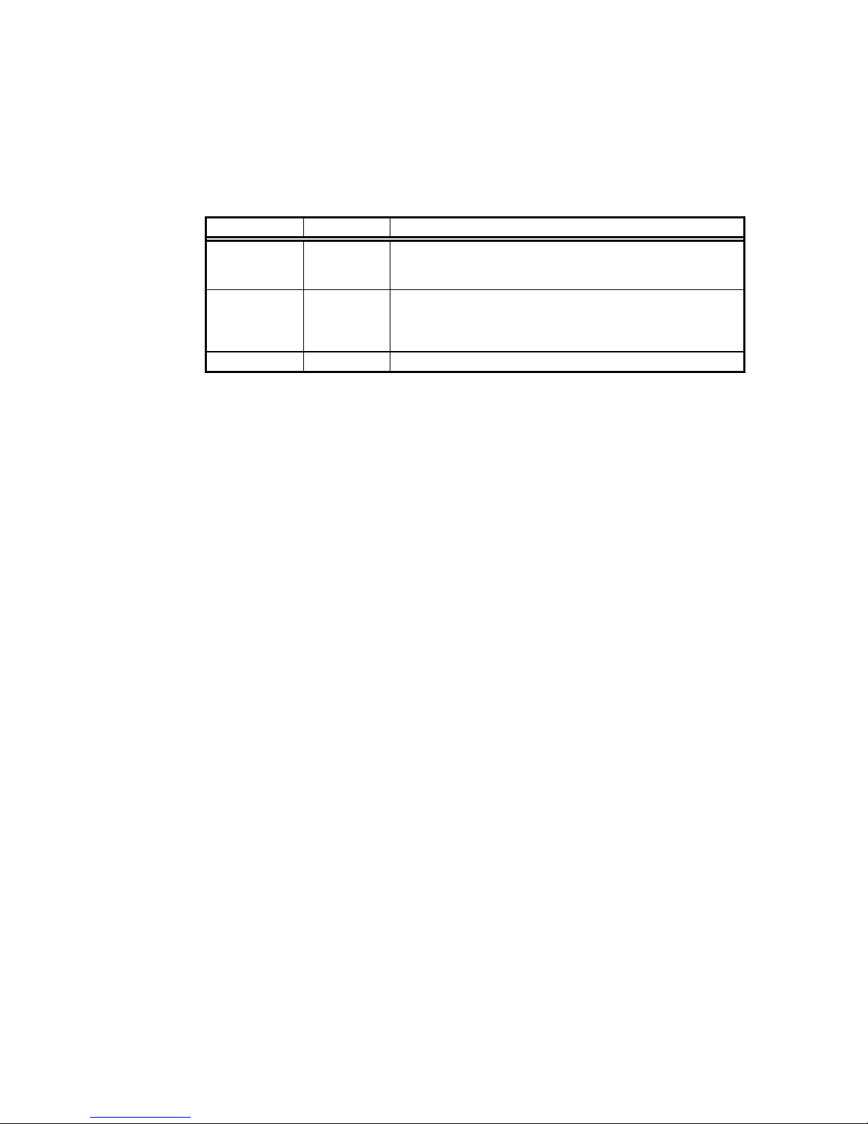
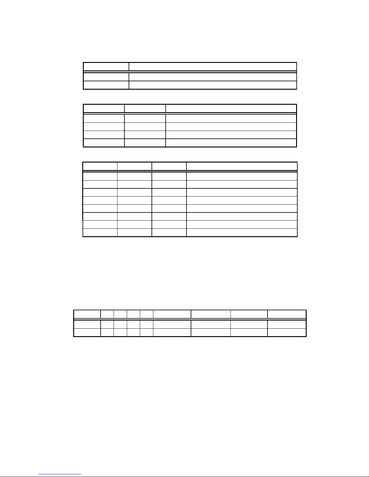
1.1. NUMERIC NOTATION
This manual represents numbers according to the notation described in the following table.
Hexadecimal and binary numbers are hyphenated at every four digits, if they are difficult to read
because of many digits being in each number.
Number Notation rule Example
Decimal number Only numerals are indicated. “ 10” represents number 10 in decimal.
Hexadecimal number A number is suffixed with letter H. “ 10H” represents number 16 in
decimal.
Binary number A number is suffixed with letter B. “ 10B” represents number 2 in decimal.
Number Notation Rules
Page 7

RTE-V852-PC USER’ S MANUAL (Rev. 1.10)
6
2. FEATURES AND FUNCTIONS
The overview of each function block of the RTE-V852-PC is shown below. The RTE-V852-PC
consists of the Socket board (smaller board) on which the CPU is mounted, and the Base board on
which other components and the Socket board are mounted.
V852
ISA Bus
Base Board
Local Bus
Socket Board
ISA BUS I/F
JEXT
CONNECTOR
D-RAM
S-RAM
ROM
SIO/PRT
RS-232C
CONNECTOR
TIMER
USER
HW
PARALLEL
CONNECTOR
Internal
Control
FPGA
RS-232C
CONNECTOR
RTE-V852-PC Block Diagram
Features
• ROM: Standard 128 Kbytes (64K × 16-bit EPROM × 1)
Maximum 512 Kbytes (128K × 16-bit EPROM × 1)
• SRAM: 512 Kbytes (64K × 16-bit SRAM × 4)
• DRAM: 4, 8 or 16 Mbytes (standard 4 Mbytes) installed in one 72-pin SIMM socket
The EDO-type DRAM-SIMM can be used as well as the ordinary type DRAM-SIMM.
• RS-232C port (9-pin D-SUB connector × 1, 10-pin 2.54 mm pin header × 2)
• Parallel port (26-pin 2.54-mm pin header × 1)
• Communication function supported using the ISA bus of a PC/AT or compatible
• Local bus connector for user-installed expansion equipment
• Releases CPU ports for the connector.
• External reset switch provided on the rear panel
• Connection pins for ROM in-circuit debugger
Page 8
RTE-V852-PC USER’ S MANUAL (Rev. 1.10)
7
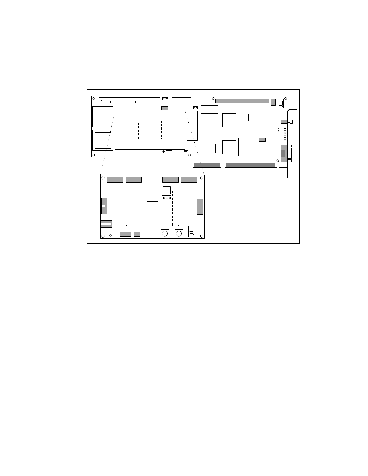
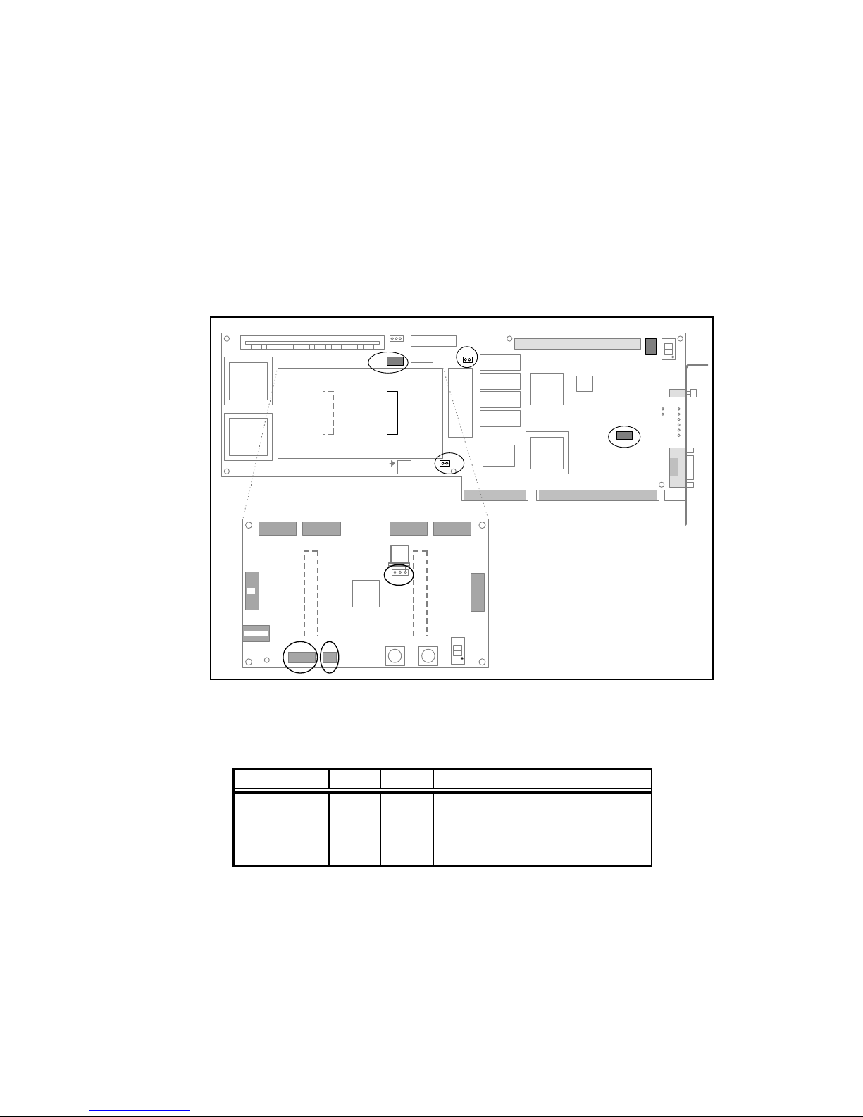
3. BOARD CONFIGURATION
The physical layout of the major components on the RTE-V852-PC board is shown below. This
chapter explains each component. To use the board with the Multi debugger, first read Chapter 4
before reading this chapter.
SW2
SIO/PRT
SW_RESET
JPOWER
JEXT
JSIO1
PLD
PLD
SW1
ROM
RAM
NMI-
GND
TIMER
RESET-
JPRT
JSIO2
J5
J6
JROMEM
OSC1
1pin
JP1
SIM-72pin
POWER
ISAIO
ISAMEM
ROM
SRAM
DRAM
TOVER
NMI_SW
P3MODE
PLLSEL
CKSEL
P07
P05
P04
P03
P02
P01
P00
P06
MODE1
RESET_SW
NMI_SW
POWER
JPORT3
SW2
SW1
RESET_SW
WAIT
PLD
Base Board
Socket Board
Socket Board
RAM
RAM
RAM
PLD
JP2
J3J1J2
JPOWER
JP1
Xtal
V852
JPORT10
JPORT1
JPORT0
JPORT2
RTE-V852-PC Board Top View
3.1. RESET SWITCH [SOCKET BOARD] (RESET_SW)
RESET_SW on the Socket board is the reset switch. Pressing this switch resets the CPU, and
causes the reset signal to be supplied to the Base board. This switch has the same function as the
reset switch on the Base board.
3.2. RESET SWITCH [BASE BOARD] (SW_RESET)
SW_RESET on the Base board is the reset switch. Pressing this switch resets the CPU. This
switch has the same function as the reset switch on the Socket board.
3.3. NMI SWITCH [SOCKET BOARD] (NMI_SW)
NMI_SW on the Base board is the NMI switch. Pressing this switch causes the level of the NMI pin
of the CPU to go Low. As the NMI signal is also provided by the Base board, the NMI signal from this
switch is ORed with the NMI signal from the Base board (see Section 9.2).
Page 9
RTE-V852-PC USER’ S MANUAL (Rev. 1.10)
8
3.4. POWER SUPPLY CONNECTOR [SCOKET/BASE BOARD] (JPOWER)
When this board is to be used as a standalone, that is, without being inserted in an ISA bus slot, the
board should be supplied with power from an external power supply by connecting it to the JPOWER
connector.
JPOWER connectors are provided both on the Socket board and on the Base board, but it is
recommended that the JPOWER connector on the Base board be used.
The external power should be one rated as listed below.
Voltage: 5 V
Current: Maximum of 2 A (excluding the current supplied to the JEXT connector)
Mating connector: Type A (5.5 mm in diameter)
Polarity:
GND
GND
+5 V
+5 V
[Caution] When attaching an external power supply to the board, be careful about its connector
polarity. When inserting the board into the ISA bus slot, do not attach the JPOWER
connector to an external power supply.
Page 10
RTE-V852-PC USER’ S MANUAL (Rev. 1.10)
9
3.5. PROCESSOR PIN CONNECTORS [SOCKET BOARD]
(JPORT0, JPORT1, JPORT2, JPORT3, JPORT10)
The pins of the CPU are inserted into these connectors. For details of the connections within the
board, see Chapter 13.
JPORT0
pin No.
Signal name
JPORT0
pin No.
Signal name
1 GND 2 GND
3 P07/INTP13 4 P06/INTP12
5 P05/INTP11 6 P04/INTP10
7 P03/TI1 8 P02/TCLR1
9 P01/TO11 10 P00/TO10
JPORT0 Pin Arrangement
JPORT1
pin No.
Signal name
JPORT1
pin No.
Signal name
1 GND 2 GND
3 P17 4 P16
5 P15 6 P14
7 P13 8 P12
9 P11 10 P10
JPORT1 Pin Arrangement
JPORT2
pin No.
Signal name
JPORT2
pin No.
Signal name
1 GND 2 GND
3 P27/SCK2- 4 P26/SI2
5 P25/SO2 6 P24/INTP03
Note
7 P23/INTP02
Note
8 P22/INTP03
Note
9 P21/INTP03
Note
10 NC.
JPORT2 Pin Arrangement
JPORT3
pin No.
Signal name
JPORT3
pin No.
Signal name
1 GND 2 GND
3 P37/SCK1 4 P36/SI1
5 P35/SO1 6 P34/RXD
7 P33/TXD 8 P32/SCK09 P31/SI0 10 P30/SO0
JPORT3 Pin Arrangement
JPORT10
pin No.
Signal name
JPORT10
pin No.
Signal name
1 GND 2 GND
3 NC. 4 NC.
5 NC. 6 NC.
7 P103 8 P102
9 P101/HLDRQ- 10 P100/HLDAK-
JPORT10 Pin Arrangement
Note See Section 3.15.
Page 11
RTE-V852-PC USER’ S MANUAL (Rev. 1.10)
10
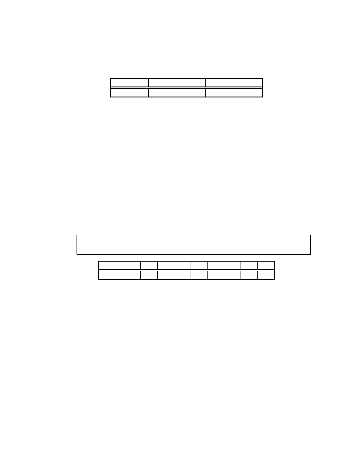
3.6. PROCESSOR PIN CONNECTORS [SOCKET BOARD/BASE BOARD] (J1, J2/J5, J6)
These connectors are used to connect the Socket board to the Base board.
J1/J5 pin No. Signal name J1/J5 pin No. Signal name
1 GND 2 GND
3 P57/AD15 4 P56/AD14
5 P55/AD13 6 P54/AD12
7 P53/AD11 8 P52/AD10
9 P51/AD9 10 P50/AD8
11 GND 12 GND
13 P47/AD7 14 P46/AD6
15 P45/AD5 16 P44/AD4
17 P43/AD3 18 P42/AD2
19 P41/AD1 20 P40/AD0
21 P22/INTP01 22 P21/INTP00
23 RTE_CON-(IN) 24 1M/16M-(OUT)
25 +5V(IN) 26 +5V(IN)
J1/J5 Pin Arrangement
J2/J6 pin No. Signal name J2/J6 pin No. Signal name
1 GND 2 GND
3 GND(A23) 4 GND(A22)
5 GND(A21) 6 GND(A20)
7 P63(A19) 8 P62(A18)
9 P61(A17) 10 P60(A16)
11 GND 12 GND
13 CLKOUT 14 X1(IN)
15 RESET-(IN/OUT) 16 WAIT17 NMI 18 P96/HLDRQ19 P95/HLDAK- 20 P94/ASTB
21 P93/DSTB- 22 P92/R_W23 P91/UBEN- 24 P90/LBEN25 P24/INTP03 26 P23/INTP02
J2/J6 Pin Arrangement
Page 12
RTE-V852-PC USER’ S MANUAL (Rev. 1.10)
11
3.7. SERIAL CONNECTOR [SOCKET BOARD] (J3)
The J3 connector is used for the RS-232C interface, controlled by the UART built into the CPU. The
pins of this connector have a pitch of 2.54 mm, and the pin arrangement is identical to that of the 9pin D-SUB RS-232C connector normally provided on the PC/AT when using a push-fit connector with
a ribbon cable. All signals at this connector are converted to the RS-232C level.
The pin arrangement of the J3 connector is shown below, after which the signal assignment is listed.
For details of the wiring of the connection signals when the board is connected to a PC (or host), see
the table in Section 3.20.
1109876543
2
J3 Pin Arrangement
J3 pin No. Signal name Input/output Corresponding port
1 NC Input
3 RxD(RD) Input P34
5 TxD(SD) Output P33
7
DTR(DR)
Note
Output -9 GND
2 DSR(ER) Input P37
4 RTS(RS) Output P35
6 CTS(CS) Input P36
8 NC
10 NC
J3 Connector Signals
Note The DTR signal outputs the active level at power-on.
Page 13
RTE-V852-PC USER’ S MANUAL (Rev. 1.10)
12
3.8. SWITCH 1 [SOCKET BOARD] (SW1)
SW1 on the Socket board is the switch used for setting the mode.
SW1 contact 1 2 3 4
Port MODE CKSEL PLLSEL P3MODE
SW1-to-Port Correspondence
MODE1: Switch for specifying the operation mode of the V852.
OFF: Single chip mode
ON: ROM-less mode (factory-set)
CKSEL: Switch for specifying the CKSEL level of the V852.
OFF: Direct mode
ON: PLL mode (factory-set)
PLLSEL: Switch for specifying the PLLSEL level of the V852.
OFF: × 5 (factory-set)
ON: × 1
P3MODE: Switch for specifying the mode used by P3 of the V852.
OFF: Connects P34, P36, and P37 to JPORT3. (factory-set)
ON: Connects P34, P36, and P37 to J3 (RS-232C).
3.9. SWITCH 2 [SOCKET BOARD] (SW2)
SW2 on the Socket board is connected to CPU Port 0 and can be used freely by the user. When a
switch contact is OFF, it represents 1. When it is ON, it represents 0.
[Caution] Set all of the switch contacts to OFF when the P0 terminal is to be used for other
purposes.
SW2 contact 1 2 3 4 5 6 7 8
Port P00 P01 P02 P03 P04 P05 P06 P07
SW2-to-Port Correspondence
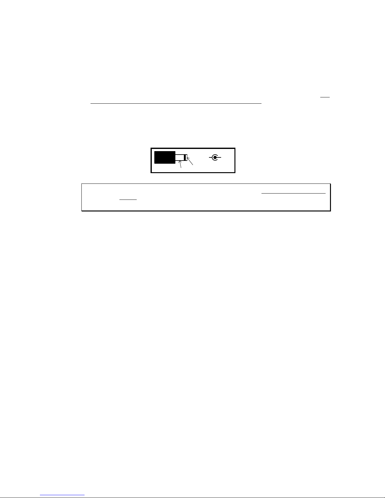
3.10. CRYSTAL SOCKET [SOCKET BOARD] (JP1)
JP1 has two roles. Namely, it is used to select the clock supplied to the CPU and also acts as the
connector for the crystal oscillator.
When an oscillator is connected to the OSC1 socket on the Base board:
Jumper pins 1 and 2 of JP1. Do not connect a crystal oscillator to JP1 in this case.
When a crystal oscillator is connected to JP1:
Connect the crystal oscillator across pins 1 and 3. Do not jumper pins 1 and 2.
Page 14
RTE-V852-PC USER’ S MANUAL (Rev. 1.10)
13
3.11. 7-SEGMENT LED [SOCKET BOARD] (LED_P1)
LED_P1 is a 7-segment LED, to which the P1 ports of the CPU are connected as shown in the table
below. When a bit is set to 1, the corresponding segment lights.
Segment A B C D E F G D.P.
Port P10 P11 P12 P13 P14 P15 P16 P17
LED_P1 Correspondence
A
B
C
D
E
F
G
DP
3.12. LEDS [SOCKET BOARD]
The table below explains the LEDs on the Socket board.
Name Description
LED_POWER Lights when power is supplied to the board.
LED Status
3.13. SWITCH 1 [BASE BOARD] (SW1)
SW1 is the switch connected to the general-purpose input ports and read by software. When a switch
contact is OFF, it represents 1. When it is ON, it represents 0. See Sections 4.1 and 6.5 for details.
3.14. SWITCH 2 [BASE BOARD] (SW2)
SW2 is the switch used for selecting the I/O address of the ISA bus. Switch contacts 1 to 8
correspond to A4 to A11 of the ISA bus address (A12 to A15 are fixed at 0). Therefore, this switch
can be used to select an I/O address in the range of 000xH to 0FFxH. When a switch contact is OFF,
it represents 1. When it is ON, it represents 0 (see Section 4.1).
SW2 contact 1 2 3 4 5 6 7 8
Address A4 A5 A6 A7 A8 A9 A10 A11
SW2-to-Address Correspondence
Page 15
RTE-V852-PC USER’ S MANUAL (Rev. 1.10)
14
3.15. SWITCH 3 [BASE BOARD] (SW3)
SW3 is the switch used for selecting whether the interrupt factors on the Base board are to be
connected to the CPU. The relationship between the switch contact numbers, CPU interrupt pins
and interrupt factors is given in the table below. When a switch contact is OFF, it represents no
connection. When it is ON, it represents connection to the CPU.
When a signal having the same pin name as one of the CPU pin names listed below is transmitted
through the JPORT2 connector, set the corresponding contact of SW3 to OFF.
Usually, set all of the switch contacts to OFF. For INT0SEL and INT1SEL, see Section 9.3.
SW3
contact
CPU pin name J5/J6 pin No. Interrupt factor
1 P21/INTP00 J5-Pin 22 Interrupt request of UART2(SCC2) of TL16C552A
on Base board. Interrupt is High level.
2 P22/INTP01 J5-Pin 21 Interrupt request on Base board that is selected
with INT0SEL. Interrupt is High level.
3 P23/INTP02 J6-Pin 26 Inverted signal of JEXT bus interrupt request
signal (INT-). Interrupt is High level.
4 P24/INTP03 J6-Pin 25 Interrupt request on Base board that is selected
with INT1SEL. Interrupt is High level.
SW3-to-Interrupt Correspondence
3.16. ROM CAPACITY SWITCHING JUMPER [BASE BOARD] (JP1)
JP1 is the jumper to be set according to the capacity of the mounted ROM. Leave it open when
mounting 128 Kbytes (64K × 16-bit) or 256 Kbytes (128K × 16-bit) of ROM. Close the jumper when
mounting 512 Kbytes (256K × 16-bit) of ROM.
3.17. ISA BUS INTERFACE SWITCHING JUMPER [BASE BOARD] (JP2)
JP2 is the jumper for switching the mode of the interface with the ISA bus. This jumper should
normally be left open.
3.18. LEDS [BASE BOARD]
These LEDs are used for status indication. The LEDs are explained in detail in the table below.
Name Description
POWER Lights when power is supplied to the board.
ROM Lights when the ROM area is selected.
SRAM Lights when the SRAM area is selected.
DRAM Lights when the DRAM area is selected.
TOVER Lights when a time-over ready interrupt occurs and remains lit until the
time-over ready interrupt is cleared by software. (See Section 12.1.)
WAIT Lights when a wait cycle occurs as a result of a cycle being generated in
the external extension bus. The brightness of the LED corresponds to
the wait cycle frequency.
ISAMEM Lights when the ISA memory area is selected.
ISAIO Lights when the ISA I/O area is selected.
LED Status
Page 16
RTE-V852-PC USER’ S MANUAL (Rev. 1.10)
15
3.19. TEST PINS FOR ROM EMULATION [BASE BOARD] (JROMEM)
JROMEM are the test pins used to connect a ROM in-circuit type debugger. These test pins accept
control signals from the ROM in-circuit debugger. The signal names and functions are listed in the
table below.
Signal name Input/output Function
RESET- Input Connects the reset request signal from the ROM in-circuit
debugger. The CPU is reset when a Low level signal is input.
The input is pulled up by a 1 kΩ resistor on the board.
NMI- Input Connects the NMI request signal (break request) from the ROM
in-circuit debugger. The NMI is input to the CPU when a Low
level signal is input. The input is pulled up by a 1 kΩ resistor on
the board. (See Section 9.2.)
GND
Ground pin to ground the ROM in-circuit debugger.
Test Pin Functions
Page 17
RTE-V852-PC USER’ S MANUAL (Rev. 1.10)
16
3.20. SERIAL CONNECTORS [BASE BOARD] (JSIO1, JSIO2)
The JSIO1 and JSIO2 connectors are used for the RS-232C interface controlled by the serial
controller (TL16C552A). Regarding the connector shapes, JSIO1 is a 9-pin D-SUB RS-232C
connector like that normally provided on the PC/AT, while JSIO2 is a pin header type connector with a
pitch of 2.54 mm. All signals at both of these connectors are converted to RS-232C level. The pin
arrangements of these connectors are shown below, after which the signal assignments are listed.
For the connection signals when the connectors are connected to the host, the table lists the wiring for
both the D-SUB 9 pins and D-SUB 25 pins on the host side. (Regular cross-cable wiring is used for
these connections.)
The pin arrangement of JSIO2 is identical to that of JSIO1 when a push-fit connector with a ribbon
cable is connected to JSIO2.
198765432
JSIO1 Pin Arrangement
1109876543
2
JSIO2 Pin Arrangement
Connector pin No. on the host sideJSIO1
pin No.
JSIO2
pin No.
Signal
name
Input/output
D-SUB9 D-SUB25
1 1 DCD Input
2 3 RxD(RD) Input 3 2
3 5 TxD(SD) Output 2 3
4 7 DTR(DR) Output 1, 6 6, 8
5 9 GND 5 7
6 2 DSR(ER) Input 4 20
7 4 RTS(RS) Output 8 5
8 6 CTS(CS) Input 7 4
9 8 RI Input
-- 10 NC
JSIO1/2 Connector Signals
Page 18

RTE-V852-PC USER’ S MANUAL (Rev. 1.10)
17
3.21. PARALLEL CONNECTOR [BASE BOARD] (JPRT)
The JPRT connector is used for the parallel interface controlled by the parallel (printer) controller
(TL16C552A). It is a pin header type connector with a pitch of 2.54 mm. All signals at this
connector are at the RS-232C level. Its pin arrangement and signal assignment are shown and
listed below.
The pin arrangement of JPRT is identical to the 25-pin D-SUB connector like that normally provided
on the PC/AT when a push-fit connector with a ribbon cable is used.
1
2625242322212019181716151413121110
9876543
2
JPRT Pin Arrangement
JPRT
pin No.
Signal
name
JPRT
pin No.
Signal
name
1 STB- 2 AUTO_FD3 D0 4 ERROR5 D1 6 INIT7 D2 8 SELECT_IN-
9 D3 10 GND
11 D4 12 GND
13 D5 14 GND
15 D6 16 GND
17 D7 18 GND
19 ACK- 20 GND
21 BUSY 22 GND
23 PE 24 GND
25 SELECT 26 NC
JPRT Connector Signals
3.22. EXTENSION BUS CONNECTOR [BASE BOARD] (JEXT)
The JEXT connector is provided to enable the extension of memory or I/O. This connector is
internally connected to the local bus of the Base board. For details of this connector, see Chapter 8.
3.23. CLOCK SOCKET [BASE BOARD] (OSC1)
The OSC1 socket is connected to an oscillator used to supply clock pulses to the CPU. At the
factory setting, the V852 uses a PLL for generating the system clock, and the CPU clock frequency is
five times that of the oscillator connected to the OSCI socket.
The clock supplied to the CPU can also be obtained from a crystal oscillator connected to JP1 on the
Socket board. (See Section 3.10).
The oscillator connected to the OSC1 socket must be of an 8-pin DIP type (half type).
[Caution] When the OSC1 socket is used, short pins 1 and 2 of JP1 on the socket board.
Page 19

RTE-V852-PC USER’ S MANUAL (Rev. 1.10)
18
3.24. DRAM-SIMM SOCKETS
A 4-Mbyte SIMM is mounted in the DRAM-SIMM socket as standard. This socket can hold a 72-pin
SIMM (known as a module in the case of DOS/V machines) with a capacity of 4 or 8 Mbytes, and can
also accept an EDO type DRAM-SIMM in addition to normal DRAM-SIMMs. Select a DRAM that
satisfies the access timing requirements by referring to Section 7.3. The capacity of the connected
SIMM can be read through the PIO port. (See Section 6.6.)
3.25. ROM SOCKETS
The RTE-V852-PC has ROM sockets to hold 40-pin ROM chips to provide standard 128 Kbytes (64K
× 16 bits). When the standard ROM is replaced to enable the use of a Multi debugger, connect ROM
having an access time of no more than 150 ns. When mounting RAM of a different capacity, it may
sometimes be necessary to switch JP1 on the Base board. (See Section 3.16.)
Page 20
RTE-V852-PC USER’ S MANUAL (Rev. 1.10)
19
4. INSTALLATION AND USE
The RTE-V852-PC board is designed to be installed in the ISA bus slot of a PC/AT or compatible
(hereafter called the PC). However, it can also be used as a standalone, if it is powered from an
external power supply. When the board is used for testing purposes or with the Multi debugger,
communication software called RTE for Windows must be installed in the PC. Refer to the RTE for
Windows Installation Manual for installation and test methods.
4.1. BOARD SETTING
The RTE-V852-PC board has DIP switches. The DIP switches can be used to set up the evaluation
board. The switch layout is shown below.
Switches on the RTE-V852-PC Board
SW1 on the Base board is a switch for general-purpose input ports. For the Multi monitor in the
factory-installed ROM, SW1 is used to set the RS-232C baud rate and profiler timer period.
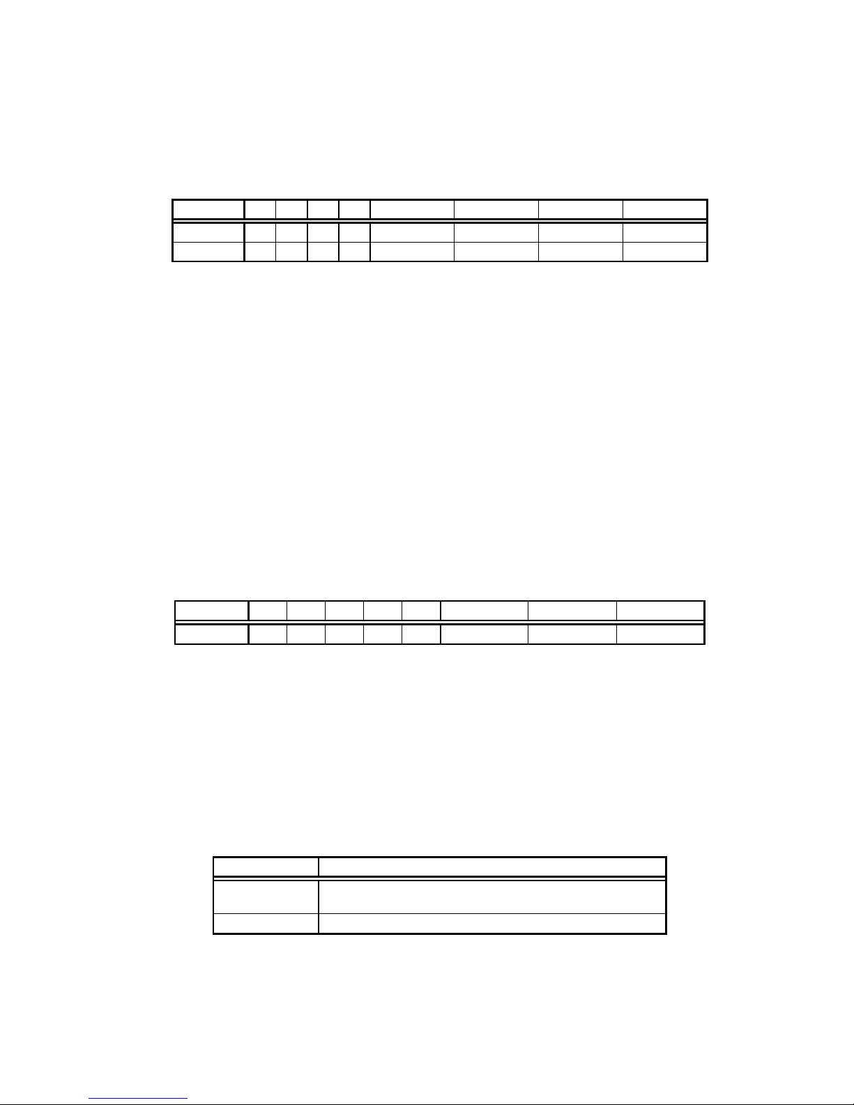
SW1 contact 1 2 Baud rate
Setting ON
OFF
ON
OFF
ON
ON
OFF
OFF
Not used
38400 baud
19200 baud
9600 baud (factory-set)
Baud Rate Setting
SW2
SIO/PRT
SW_RESET
JPOWER
JEXT
JSIO1
PLD
PLD
SW1
ROM
RAM
NMI-
GND
TIMER
RESET-
JPRT
JSIO2
J5
J6
JROMEM
OSC1
1pin
JP1
SIM-72pin
POWER
ISAIO
ISAMEM
ROM
SRAM
DRAM
TOVER
WAIT
PLD
Base Board
Socket Board
RAM
RAM
RAM
PLD
JP2
NMI_SW
P3MODE
PLLSEL
CKSEL
P07
P05
P04
P03
P02
P01
P00
P06
MODE1
RESET_SW
NMI_SW
POWER
JPORT3
SW2
SW1
RESET_SW
Socket Board
J3J1J2
JPOWER
JP1
Xtal
V852
JPORT10
JPORT1
JPORT0
JPORT2
Page 21

RTE-V852-PC USER’ S MANUAL (Rev. 1.10)
20
SW1 contact 3 4 Profiler period
Setting ON
OFF
ON
OFF
ON
ON
OFF
OFF
Timer is not used.
Note
200 Hz 5 ms
100 Hz 10 ms
60 Hz 16.67 ms (factory-set)
Note: Do not set this contact when using a Multi debugger. (See Section 10.5.)
Profiler Period Setting
Contacts 5 to 8 of SW1 on the Base board are not used by the Multi monitor (they are factory-set to
OFF prior to shipment).
SW2 on the Base board is used to select the I/O bus of the ISA bus. Switch contacts 1 to 8
correspond to A4 to A11 of the address (A12 to A15 are fixed at 0). Therefore, this switch can be
used to select an I/O address in the range of 000xH to 0FFxH. When a switch contact is OFF, it
represents 1. When it is ON, it represents 0. The address is usually set to between 20xH and 3FxH.
SW2 contact
1 2 3 4 5 6 7 8
Address A4 A5 A6 A7 A8 A9 A10 A11 I/O Address
ON/
OFF
0 0 0 0 0
1
0 0 020xH
(factory-set)
I/O Address Correspondence
SW3 on the Base board is set to ON when the interrupt request line on the Base board is connected to
a CPU pin. Normally, set all of contacts 1 to 4 to OFF. (See Section 3.15.)
JP1 and JP2 on the Base board should normally be left open. JP1 may have to be switched when
ROM having a different capacity from the standard is mounted. (See Sections 3.16 and 3.17.)
SW1 on the Socket board is used to select the CPU mode and the connection of CPU Port 2 (see
Section 3.8). The default settings are listed in the tables below.
SW1-1 Description
ON Sets the operation mode of the V852 to ROM-less. (Built-in
ROM is disabled and the external extension bus is enabled.)
SW1-2 Description
ON (CKSEL = Low)
SW1-3 Description
OFF (PLLSEL = High)
SW1-4 Description
OFF (Connects P34, P36, and P37 to JPORT2.)
SW2 on the Socket board selects the level of the signals supplied to Port 0 and can be used as
desired by the user. The factory-set default is all OFF (see Section 3.9).
JP1 on the Socket board determines the clock supplied to the CPU. Connect a 6.6-MHz crystal
Page 22

RTE-V852-PC USER’ S MANUAL (Rev. 1.10)
21
oscillator to JP1. When the clock must be changed, see Section 3.10.
Page 23

RTE-V852-PC USER’ S MANUAL (Rev. 1.10)
22
4.2. INSTALLATION ON THE ISA BUS
When the RTE-V852-PC is installed in the ISA bus slot of the PC, power (+5 V) is supplied from the
ISA bus to the board. In addition, the ISA bus can be used for communication with the debugger, so
programs are down-loaded at high speed.
The RTE-V852-PC can be installed in the ISA bus slot according to the following procedure.
• Set the I/O address of the PC using a DIP switch on the board. Be careful not to specify the
same I/O address as used for any other I/O unit. See Section 4.1 for switch setting.
‚ Turn off the power to the PC, open its housing, and confirm the ISA bus slot to be used. If the
slot is equipped with a rear panel, remove the rear panel.
ƒ Insert the board into the ISA bus slot. Make sure that the board does not touch any adjacent
board. Fasten the rear panel of the board to the housing of the PC with screws.
„ Turn on the power to the PC, and check that the POWER-LED on the board lights. If the LED
does not light, turn off the PC power immediately, and check the connection. If the system
does not start normally (for example, if an error occurs during installation of a device driver), it is
likely that the set I/O address is the same as one already in use. Reconfirm the I/O address of
the board by referring to the applicable manual of the PC or the board.
… When the system turns out to be normal, turn off the PC power again, and put back its housing.
4.3. STANDALONE USE OF THE BOARD
When the RTE-V852-PC is used as a standalone rather than being installed in the PC, it requires an
external power supply. In addition, communication with the debugger is supported only by the RS232C interface. This configuration is useful when the host debugger used with the board is not one
in the PC/AT or compatible as well as when the board is used for hardware confirmation and
expansion.
The RTE-V852-PC can be used as a standalone according to the following procedure.
• Get an RS-232C cable for connection with the host and an external power supply (+5 V, 2 A) on
hand. Especially for the power supply, watch for its voltage and connector polarity. In
addition, attach spacers to the four corners of the board, so it will not pose any problem wherever
it is installed. See Sections 3.20 and 3.4 for RS-232C cable connection and the power supply
connector, respectively.
‚ Set the RS-232C baud rate using a DIP switch on the board. See Section 4.1 for switch setting.
ƒ Connect the board to the host via an RS-232C cable. Also connect an external power supply to
the JPOWER connector, then check that the POWER-LED on the board lights. If the LED does
not light, turn off the power immediately, and check the connection.
Page 24
RTE-V852-PC USER’ S MANUAL (Rev. 1.10)
23
5. HARDWARE REFERENCES
This chapter describes the hardware of the RTE-V852-PC.
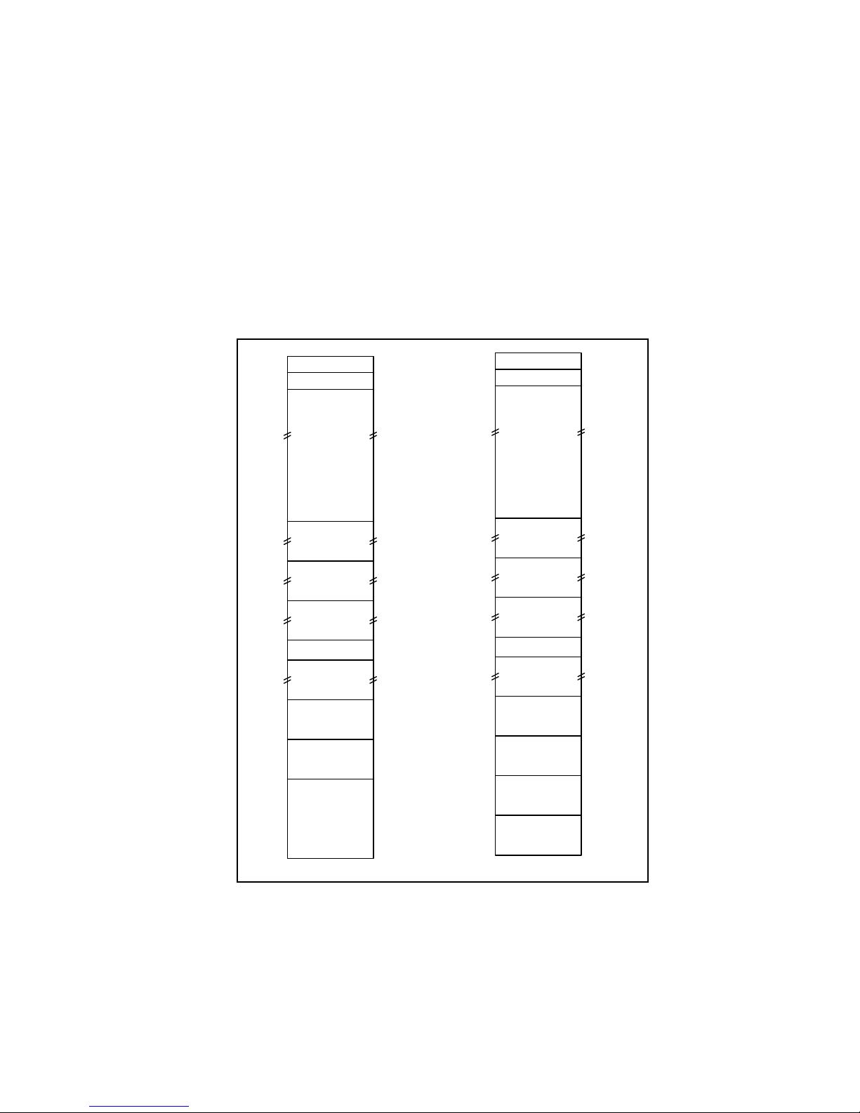
5.1 MEMORY MAP
The memory assignment of the board is shown below.
As the CPU of the V852 includes built-in resources, the built-in resources appear in place of the
external resources in those spaces where the built-in resources exist. More precisely, built-in ROM
appears between 00-0000H and 0F-FFFFH (only when the CPU is in single-chip mode), built-in RAM
appears between FF-E000H and FF-EFFFH and the built-in peripheral I/O appears between FFF000H and FF-FFFFH.
Reserved
Reserved
Access inhibited
Reserved
Reserved
7F-FFFFH
6F-FFFFH
5F-FFFFH
3F-FFFFH
3F-F000H
3F-EFFFH
80-0000H
70-0000H
60-0000H
40-0000H
20-0000H
1F-FFFFH
17-FFFFH
07-FFFFH
0F-FFFFH
18-0000H
10-0000H
08-0000H
00-0000H
SYSTEM-I/O
Access inhibited
DRAM
EXT-BUS
ROM-less mode
Built-in ROM
SRAM
ROM
Image of 00-0000H
to 07-FFFFH
(ROM)
Built-in RAM
Built-in peripheral I/O
Image of 08-0000H
to 0F-FFFFH
(SRAM)
7F-FFFFH
6F-FFFFH
5F-FFFFH
3F-FFFFH
3F-F000H
3F-EFFFH
80-0000H
70-0000H
60-0000H
40-0000H
20-0000H
1F-FFFFH
17-FFFFH
0F-FFFFH
18-0000H
10-0000H
00-0000H
FF-FFFFH
SYSTEM-I/O
DRAM
EXT-BUS
Built-in RAM
Built-in peripheral I/O
Single-chip external extended mode
SRAM
ROM
FF-E000H
FF-EFFFH
FF-F000H
FF-DFFFH
FF-FFFFH
FF-E000H
FF-EFFFH
FF-F000H
FF-DFFFH
Memory Map
Page 25

RTE-V852-PC USER’ S MANUAL (Rev. 1.10)
24
ROM space (00-0000H to 07-FFFFH, 10-0000H to 17-FFFFH)
This 512-Kbyte space is provided as ROM on the Base board. The standard ROM has a
capacity of 256 Kbytes and an access time of no more than 150 ns. The ROM is capable of
inserting wait states into the access cycle based on ready signal control, and the wait count can
be set with SYSTEM-I/O (see Section 6.7). For details of the required wait count, see Section
7.2.
The ROM on the Base board incorporates the Multi debugger monitor as standard.
SRAM space (08-0000H to 0F-FFFFH, 18-0000H to 1F-FFFFH)
This 512-Kbyte space is provided as SRAM on the Base board. The SRAM is capable of
specifying wait states and the wait count can be set with SYSTEM-I/O (see Section 6.7). For
details of the required wait count, see Section 7.2.
Reserved and access-inhibited spaces
Do not attempt to access these spaces.
SYSTEM-I/O space (3F-F000H to 3F-FFFFH)
This space is assigned to I/O devices for controlling each function on the base board. It acts as
memory-mapped I/O units. See Chapter 6 for details.
EXT-BUS space (70-0000H to 7F-FFFFH)
This space is used for a hardware extension board connected to the JEXT connector on the
board. See Chapter 8 for details of EXT-BUS.
DRAM space (80-0000H to FF-FFFFH)
This space is provided by the 72-pin SIMM mounted on the Base board. SIMM memory of 4, 8
or 16 Mbytes can be mounted. Also, an EDO-DRAM SIMM can be mounted. It is possible to
specify RAS, CAS and precharge widths (see Section 6.7). The type of the mounted SIMM can
be identified from PD[1..4] of the Status port (see Section 6.6).
Page 26

RTE-V852-PC USER’ S MANUAL (Rev. 1.10)
25
6. SYSTEM-I/O
SYSTEM-I/O is an I/O device mapped in a memory space. The I/O devices include the
UART/PRINTER, TIC, PIO, and ISA bus interface. (No description about the ISA bus interface is
included.)
6.1. SYSTEM-I/O LIST
The following table lists the SYSTEM-I/O functions.
Address Function Note
3F-F000H to 3F-F00EH Sets/references UART-CH#1 (TL16C552A)
Recovery time is required.
3F-F010H to 3F-F01EH Sets/references UART-CH#2 (TL16C552A)
Recovery time is required.
3F-F020H to 3F-F026H Sets/references PRINTER (TL16C552A)
Recovery time is required.
3F-F030H to 3F-F036H Sets/references timer controller (µPD71054)
Recovery time is required.
3F-F040H Sets Base board 7-segment LED display data
3F-F050H References Base board DIPSW1
3F-F060H References status (DRAM-PD, time-over flag, etc.)
3F-F080H Sets/references SRAM wait state
3F-F0A0H Sets/references DRAM precharge time
3F-F0B0H Sets/references DRAM RAS width
3F-F0C0H Sets/references DRAM read-cycle CAS width
3F-F0D0H Sets/references DRAM page mode
3F-F0E0H Sets/references SYSTEM-I/O wait state
3F-F0F0H Sets/references ROM wait state
3F-F100H ----------------------------------- Reserved
3F-F110H ----------------------------------- Reserved
3F-F140H to 3F-F150H Sets/references NMI selection
3F-F160H to 3F-F170H References NMI status
3F-F180H Sets/references NMI, INT0 and INT1 masking
3F-F190H Clears time-over ready flag
3F-F1A0H Clears µPD71054 TOUT0 interrupt request
3F-F200H Sets/references INT0 selection
3F-F210H Sets/references INT1 selection
3F-F220H References INT0 status
3F-F220H References INT1 status
Page 27

RTE-V852-PC USER’ S MANUAL (Rev. 1.10)
26
6.2. UART/PRINTER (TL16C552A) (3F-F000H TO 3F-F026H)
The TL16C552A (dual asynchronous communications element with FIFO) IC produced by Texas
Instruments is used as UART/PRINTER. The TL16C552A has two UART channels and one channel
of the bidirectional printer board. It incorporates a 16-character FIFO buffer in the UART reception
circuitry to minimize the possibility of an overrun error during reception.
Each register in the TL16C552A is assigned as listed below. Refer to the applicable TL16C552A
manual for the function of each register.
Address Function Read Write
3F-F000H UART-CH#1 RBR/DLL THR/DLL
3F-F002H IER/DLM IER/DLM
3F-F004H IIR FCR
3F-F006H LCR LCR
3F-F008H MCR MCR
3F-F00AH LSR LSR
3F-F00CH MSR MSR
3F-F00EH SCR SCR
3F-F010H UART-CH#2 RBR/DLL THR/DLL
3F-F012H IER/DLM IER/DLM
3F-F014H IIR FCR
3F-F016H LCR LCR
3F-F018H MCR MCR
3F-F01AH LSR LSR
3F-F01CH MSR MSR
3F-F01EH SCR SCR
3F-F020H PRINTER Read-data Write-data
3F-F022H Read-status -----
3F-F024H Read-control Write-control
3F-F026H ----- -----
TL16C552A Register Arrangement
The CLK input of the TLC16C552A is connected to the 16-MHz clock.
RD-/WR- pulse widths of 80 ns are required to access the TL16C552A. As a result, wait states
should be inserted to satisfy this condition. See Section 7.4 for details of the wait setting value, and
Section 6.7 for details of the wait setting position.
The TL16C552A requires 80 ns of command recovery time. See Section 7.5 for details of the
recovery time.
Page 28

RTE-V852-PC USER’ S MANUAL (Rev. 1.10)
27
The UART-CH#1, UART-CH#2 and PRINTER interrupts can be connected to the CPU's interrupt
ports as shown in the following table.
Interrupt source Interrupt to connected CPU
UART-CH#1 NMI- , P22/INTP01
UART-CH#2 NMI- , P21/INTP00
PRINTER NMI- , P22/INTP01
Maskable interrupts pass through DIP SW3. See Section 9.2 for details of the NMI-, and Section 9.3
for details of the maskable interrupt.
UART-CH#1 is connected to the JSIO0 connector on the rear of the Base board, UART-CH#2 is
connected to the JSIO2 connector and PRINTER is connected to JPRT. UART-CH#1 is used when
using the Multi debugger for serial communication.
The TL16C552A is reset when the system is reset (see Section 9.1).
Page 29

RTE-V852-PC USER’ S MANUAL (Rev. 1.10)
28
6.3. TIC (µPD71054) (3F-F030H TO 3F-F038H)
The µPD71054 produced by NEC is installed as a TIC. The µPD71054 is compatible with the i8254
produced by Intel. It has three timers/counters. These timers/counters are used to generate the
DRAM refresh timing and monitor timer interrupts. Each register of the TIC is assigned as listed
below.
Address
Read Write
3F-F030H COUNTER#0 COUNTER#0
3F-F032H COUNTER#1 COUNTER#1
3F-F034H COUNTER#2 COUNTER#2
3F-F036H ----- Control Word
TIC Register Arrangement
The channels of the TIC are connected as shown in the figure below.
CH#0 is connected to the NMI generator circuit and is used as the interval timer of the monitor
program. At this time, CH#0 also functions as the prescale counter for CH#1.
CH#1 can be used as required by the user program. The status of the CH#0 and CH#1 outputs can
be read from the Status port (See Section 6.6).
CH#2 is used to generate the refresh timing. Therefore, the division value of CH#2 should be set to
30 (1EH) in mode 2.
CH#0
OUT
2 MHz
GATE
µPD71054
CLK
CH#1
OUT
GATE
To NMI/INT1 generator
To Status port
DRAM refresh circuit
To Status port
CLK
CH#2
OUT
GATE
CLK
RD-/WR- pulse widths of 95 ns are required to access the µPD71054. As a result, wait states should
be inserted to satisfy this condition. See Section 7.4 for details of the wait setting value and Section
6.7 for details of the wait setting position.
The µPD71054 requires 165 ns of command recovery time. See Section 7.5 for details of the
recovery time.
The TIC is reset when the system is reset (see Section 9.1).
Page 30

RTE-V852-PC USER’ S MANUAL (Rev. 1.10)
29
6.4. 7-SEGMENT LED DISPLAY DATA OUTPUT PORT (3F-F040H [Write Only])
This port sets the data to be displayed on the 7-segment LED on the Base board. The data format is
as shown in table below. Setting a bit to 0 causes the corresponding segment to light.
Bit7 Bit6 Bit5 Bit4 Bit3 Bit2 Bit1 Bit0
DPseg Gseg Fseg Eseg Dseg Cseg Bseg Aseg
A
B
C
D
E
F
G
DP
6.5. DIPSW1 READ PORT (3F-F050H [READ ONLY])
This port is used to read the status of DIPSW1 on the Base board. The data format is as shown in
table below.
Bit7 Bit6 Bit5 Bit4 Bit3 Bit2 Bit1 Bit0
SW1-8 SW1-7 SW1-6 SW1-5 SW1-4 SW1-3 SW1-2 SW1-1
No use No use No use No use TIM1 TIM0 BPS1 BPS0
SW1-[8..1]: The status of SW1 on the Base board can be read. SW1-1 corresponds to switch
“ 1” of DIP SW1, while SW1-8 corresponds to switch “ 8” of DIP SW1. When a bit is ON, it
represents 0. When a bit is OFF, it represents 1.
Some of the DIPSW1 bits are reserved by the monitor in the ROM mounted on the Base board, as
shown in table below. However, note that these functions are defined in terms of software. This
means that, even when the switch setting is changed, these functions are not affected by this
(hardware-based) action.
BPS1 BPS0 Baud rate when Multi monitor is
used in a serial circuit
0 0 Don’ t use
0 1 38400 bps
1 0 19200 bps
1 1 9600 bps
Page 31

RTE-V852-PC USER’ S MANUAL (Rev. 1.10)
30
TIM1 TIM0 Timer rate
0 0 Timer not used
0 1 200 Hz (5 ms)
1 0 100 Hz (10 ms)
1 1 60 Hz (16.67 ms)
6.6. STATUS READ PORT (3F-F060H [READ ONLY])
Bit7 Bit6 Bit5 Bit4 Bit3 Bit2 Bit1 Bit0
TOVER_FLG-
TOUT1 TOUT0
MEM1M/16M-
PD4 PD3 PD2 PD1
PD[4..1]: The status of PD[4..1] of the DRAM (72-pin SIMM) mounted on the board can be read.
The status of PD[2..1] indicates the size of the mounted DRAM. The relationship between PD[2..1]
and the DRAM capacity is given in table below.
PD[2] PD[1] DRAM capacity
0 0 4 Mbytes
0 1 Reserved
1 0 16 Mbytes
1 1 8 Mbytes
PD[2..1] and DRAM Capacity
MEM1M/16M-: “ 0” is read when the external address space of the CPU of the Socket board is
16 Mbytes, and “ 1” is read when it is 1 Mbyte.
TOUT0, TOUT1: The status of the output terminals of channels 0 and 1 of the TIC (µPD71054)
can be read (see Section 6.3).
TOVER_FLG-: This goes to “ 0” upon a time-out ready occurrence once the bus cycle count
has reached 31 cycles. Use TOVER_RDY_INT_CLR (3F-F190H) to clear this
flag (return it to “ 1” ).
Page 32

RTE-V852-PC USER’ S MANUAL (Rev. 1.10)
31
6.7. BIC (BUS INTERFACE CONTROL) (3F-F080H TO 3F-F0F0H)
The BIC is used to set the parameters related to access to ROM, SRAM, DRAM and the ports on the
Base board.
Address Bit7 Bit6 Bit5 Bit4 Bit3 Bit2 Bit1 Bit0
3F-F080H ---- ---- ---- ---- ---- ---- SRAMWAIT1 SRAMWAIT0
3F-F090H ---- ---- ---- ---- ---- ---- ---- ---3F-F0A0H ---- ---- ---- ---- ---- ---- PRCWIDE1 PCRWIDE0
3F-F0B0H ---- ---- ---- ---- ---- ---- RASWIDE1 RASWIDE0
3F-F0C0H ---- ---- ---- ---- ---- ---- CASRDWIDE1 CASRDWIDE0
3F-F0D0H ---- ---- ---- ---- ---- ---- ---- PAGEMODE
3F-F0E0H ---- ---- ---- ---- ---- ---- SYSIOWAIT1 SYSIOWAIT0
3F-F0F0H ---- ---- ---- ---- ---- ROMWAIT2 ROMWAIT1 ROMWAIT0
SRAMWAIT1 SRAMWAIT0 Function
0 0 Sets the wait count for SRAM access to 0.
0 1 Sets the wait count for SRAM access to 1.
1 0 Sets the wait count for SRAM access to 2.
1 1 Sets the wait count for SRAM access to 3.
These are reset to [1,1] when the system is reset.
PRCWIDE1 PRCWIDE0 Function
0 0 Sets the RAS precharge time for DRAM access to 1 clk.
0 1 Sets the RAS precharge time for DRAM access to 2 clks.
1 0 Sets the RAS precharge time for DRAM access to 3 clks.
1 1 Sets the RAS precharge time for DRAM access to 4 clks.
These are reset to [1,1] when the system is reset.
RASWIDE1 RASWIDE0 Function
0 0 Sets the Low width of RAS for DRAM access to 1 clk.
0 1 Sets the Low width of RAS for DRAM access to 2 clks.
1 0 Sets the Low width of RAS for DRAM access to 3 clks.
1 1 Sets the Low width of RAS for DRAM access to 4 clks.
These are reset to [1,1] when the system is reset.
CASRDWIDE1 CASRDWIDE0 Function
0 0 Sets the Low width of CAS for DRAM read access to 1 clk.
0 1 Sets the Low width of CAS for DRAM read access to 2 clks.
1 0 Sets the Low width of CAS for DRAM read access to 3 clks.
1 1 Sets the Low width of CAS for DRAM read access to 4 clks.
These are reset to [1,1] when the system is reset.
Page 33
RTE-V852-PC USER’ S MANUAL (Rev. 1.10)
32
PAGEMODE Function
0 DRAM is not used in page mode.
1 DRAM is used in page mode.
This is reset to [0] when the system is reset.
SYSIOWAIT1 SYSIOWAIT0 Function
0 0 (Sets the wait count for SYSTEM-I/O access to 8.)
0 1 Sets the wait count for SYSTEM-I/O access to 1.
1 0 Sets the wait count for SYSTEM-I/O access to 2.
1 1 Sets the wait count for SYSTEM-I/O access to 3.
These are reset to [1,1] when the system is reset.
ROMWAIT2 ROMWAIT1 ROMWAIT0 Function
0 0 0 Sets the wait count for ROM access to 8.
0 0 1 Sets the wait count for ROM access to 1.
0 1 0 Sets the wait count for ROM access to 2.
0 1 1 Sets the wait count for ROM access to 3.
1 0 0 Sets the wait count for ROM access to 4.
1 0 1 Sets the wait count for ROM access to 5.
1 1 0 Sets the wait count for ROM access to 6.
1 1 1 Sets the wait count for ROM access to 7.
These are reset to [1,1,1] when the system is reset.
See Chapter 7 for details of the recommended settings related to the wait state and DRAM.
See Section 12.2 for an explanation of the significance of the DRAM-related settings.
6.8. NMI SELECT PORT (3F-F140H TO 3F-F150H)
This port controls the generation of the NMI signal. See Section 9.2 for details of the NMI signal
generation logic.
Address Bit7 Bit6 Bit5 Bit4 Bit3 Bit2 Bit1 Bit0
3F-F140H ---- ---- ---- ----
ISACOM_NMIEN
PRT_NMIEN
UART2_NMIEN UART1_NMIEN
3F-F150H ---- ---- ---- ---- Reserved (0) TIMER_NMIEN
TOVER_NMIEN EXTBUS_NMIEN
Set each bit to “ 1” when NMI is to be generated according to the corresponding interrupt request, or
to “ 0” when NMI need not be generated.
UART1_NMIEN: Interrupt request issued by UART-CH#1 of TL16C552A
UART2_NMIEN: Interrupt request issued by UART-CH#2 of TL16C552A
PRT_NMIEN: Interrupt request issued by PRINTER of TL16C552A
ISACOM_NMIEN: Interrupt request based on communication with ISA bus
EXTBUS_NMIEN: Interrupt request received from EXTBUS
TOVER_NIMEN: Interrupt request resulting from time-over ready occurrence
TIMER_NIMEN: Interrupt request issued by TOUT0 of µPD71054
Page 34

RTE-V852-PC USER’ S MANUAL (Rev. 1.10)
33
Reserved (0): This bit is reserved and should be set to “ 0” .
Page 35
RTE-V852-PC USER’ S MANUAL (Rev. 1.10)
34
6.9. NMI STATUS PORT (3F-F160H TO 3F-F170H [READ ONLY])
This port is used to identify the source of an NMI request. See Section 9.2 for details of the NMI
signal generation logic.
Address Bit7 Bit6 Bit5 Bit4 Bit3 Bit2 Bit1 Bit0
3F-F160H ---- ---- ---- ---- ISACOM_NMI PRT_NMI UART2_NMI UART1_NMI
3F-F170H ---- ---- ---- ---- ---- TIMER_NMI TOVER_NMI EXTBUS_NMI
Each bit is set to “ 1” when NMI is generated by the corresponding interrupt request, or set to “ 0”
when it need not be generated. Each bit represents the interrupt request status of each interrupt
request source and is not affected by the settings of the NMI enable port. Therefore, the interrupt
factor causing the NMI occurrence can be identified by ANDing the information in the NMI status port
with that in the NMI select port.
UART1_NMI: Interrupt request issued by UART-CH#1 of TL16C552A
UART2_NMI: Interrupt request issued by UART-CH#2 of TL16C552A
PRT_NMI: Interrupt request issued by PRINTER of TL16C552A
ISACOM_NMI: Interrupt request based on communication with ISA bus
EXTBUS_NMI: Interrupt request received from JEXT bus
TOVER_NMI: Interrupt request resulting from time-over ready occurrence
TIMER_NMI: Interrupt request issued by TOUT0 of µPD71054
6.10. NMI/INT0/INT1 MASK PORT (3F-F180H)
This port controls the final masking of NMI, INT0 and INT1. See Section 9.2 for details of the NMI
signal generation logic and Section 9.3 for the maskable interrupt generation logic.
Address Bit7 Bit6 Bit5 Bit4 Bit3 Bit2 Bit1 Bit0
3F-F180H ---- ---- ---- ---- ---- INT1_MASK INT0_MASK NMI_MASK
NMI_MASK: Set “ 1” to mask the NMI signal to the CPU or “ 0” when it need not be
masked.
INT0_MASK: Set “ 1” to mask the INT0(P22/INTP01) signal to the CPU or “ 0” when it need
not be masked.
INT1_MASK: Set “ 1” to mask the INT1 (P24/INTP03) signal to the CPU or “ 0” when it
need not be masked.
6.11. NMI/INT1 REQUEST CLEAR PORTS (3F-F190H, 3F-F1A0H [WRITE ONLY])
When there are latched interrupts among the NMI/INT1 request factors, these ports allow the latched
requests to be cleared.
Address Write
3F-F190H Clears the NMI/INT1 request resulting from the time-over ready
occurrence (see Section 12.1).
3F-F1A0H
Clears the NMI/INT1 request issued by TOUT0 of µPD71054.
Page 36

RTE-V852-PC USER’ S MANUAL (Rev. 1.10)
35
6.12. INT0(P22/INTP01) SELECT PORT (3F-F200H)
This port controls the generation of the INT0(P22/INTP01) signal. See Section 9.3 for details of the
INT0 signal generation logic.
Address Bit7 Bit6 Bit5 Bit4 Bit3 Bit2 Bit1 Bit0
3F-F200H ---- ---- ---- ---- ---- PRT_INT0EN
ISACON_INT0EN UART1_INT0EN
Set each bit to “ 1” to generate INT0(P22/INTP01) according to the corresponding interrupt request,
or to “ 0” when it need not be generated.
UART_INT0EN: Interrupt request issued by UART-CH#1 of TL16C552A
ISACOM_INT0EN: Interrupt request based on communication with ISA bus
PRT_INT0EN: Interrupt request issued by PRINTER of TL16C552A
6.13. INT1 (P24/INTP03) SELECT PORT (3F-F210H)
This port controls the generation of the INT1 (P24/INTP03) signal. See Section 9.3 for details of the
INT0 signal generation logic.
Address Bit7 Bit6 Bit5 Bit4 Bit3 Bit2 Bit1 Bit0
3F-F210H ---- ---- ---- ---- ---- Reserved (0)
TOVER_INT1EN TIMER_INT1EN
Set each bit to “ 1” to generate INT1 (P24/INTP03) according to the corresponding interrupt request,
or to “ 0” when it need not be generated.
TIMER_INT1EN: Interrupt request issued by TOUT0 of µPD71054
TOVER_INT1EN: Interrupt request resulting from time-over ready occurrence
Reserved (0): This bit is reserved and should be set to “ 0” .
6.14. INT0(P22/INTP01) STATUS PORT (3F-F220H [READ ONLY])
This port is used to identify the source of an INT0(P22/INTP01) request. See Section 9.3 for details
of the INT0 signal generation logic.
Address Bit7 Bit6 Bit5 Bit4 Bit3 Bit2 Bit1 Bit0
3F-F220H ---- ---- ---- ---- ---- PRT_INT0 ISACON_INT0 UART1_INT0
Each bit is set to “ 1” when INT0 is generated by the corresponding interrupt request, or set to “ 0”
when it is not generated. Each bit represents the interrupt request status of each interrupt request
source and is not affected by the settings of the INT0 enable port. Therefore, the interrupt factor
causing the INT0 occurrence can be identified by ANDing the information in the INT0 status port with
that in the INT0 select port.
UART1_INT0: Interrupt request issued by UART-CH#1 of TL16C552A
ISACOM_INT0: Interrupt request based on communication with ISA bus
PRT_INT0: Interrupt request issued by PRINTER of TL16C552A
Page 37

RTE-V852-PC USER’ S MANUAL (Rev. 1.10)
36
6.15. INT1 (P24/INTP03) STATUS PORT (3F-F230H [READ ONLY])
This port is used to identify the source of an INT1 (P24/INTP03) request. See Section 9.3 for details
of the INT0 signal generation logic.
Address Bit7 Bit6 Bit5 Bit4 Bit3 Bit2 Bit1 Bit0
3F-F230H ---- ---- ---- ---- ---- ---- TOVER_INT1 TIMER_INT1
Each bit is set to “ 1” when INT1 is generated by the corresponding interrupt request, or set to “ 0”
when it need not be generated. Each bit represents the interrupt request status of each interrupt
request source and is not affected by the settings of the INT1 enable port. Therefore, the interrupt
factor causing the INT1 occurrence can be identified by ANDing the information in the INT1 status
port with that in the INT1 select port.
TIMER_INT1: Interrupt request issued by TOUT0 of µPD71054
TOVER_INT1: Interrupt request resulting from time-over ready occurrence
Page 38
RTE-V852-PC USER’ S MANUAL (Rev. 1.10)
37
7. RECOMMENDED SETTINGS
This chapter specifies the recommended values for the parameters related to access to memory
resources.
7.1. CPU SETTING
No restrictions are imposed on the settings of the bus control function built into the CPU. Therefore,
to maximize the bus performance, set DWC (0xFFFF to F060) of SFR to 0x0000 and BCC (0xFFFF to
F062) to 0x0000.
7.2. SRAM/ROM
The table below lists the recommended wait counts when SRAM and ROM with an access time of 120
ns/150 ns is used.
SRAM wait count ROM (120 ns) wait count ROM (150 ns) wait count
25 MHz 0 3 3
7.3. DRAM
The table below lists the recommended settings when DRAM with an access time of 60 ns/70 ns is
used.
Access time CPU RAS precharge time RAS width Read cycle CAS width
60 ns 25 MHz 1 CLK 2 CLKs 2 CLKs
70 ns 25 MHz 2 CLKs 2 CLKs 2 CLKs
7.4. SYSTEM-I/O WAIT COUNT
The table below lists the recommended wait counts for the SYSTEM-I/O. The SYSTEM-I/O wait
count is determined by the access time of the µPD71054, which is slowest in the SYSTEM-I/O space.
SYSTEM-I/O wait count
25 MHz 2
7.5. SYSTEM-I/O COMMAND RECOVERY TIME
Access by the TL16C552A andµPD71054 should satisfy the command recovery time requirement.
Therefore, when accessing the TL16C552A or µPD71054 continuously, a second access must be
performed a certain amount of time after the first access.
As the TL16C552A and µPD71054 share the same command signals (RD-/WR-), the recovery time is
determined by the µPD71054, this requiring the longest recovery time.
The recovery time is generated by performing read access to a memory resource other than the
TL16C552A or µPD71054. The memory resource which is recommended to be read-accessed for
generating the recovery time is the DIPSW1 read port (3F-F050H).
Page 39

RTE-V852-PC USER’ S MANUAL (Rev. 1.10)
38
Therefore, generate the DIPSW1 read port read cycles the number of times specified in the table
below, immediately after accessing the TL16C552A or µPD71054.
DIPSW1 read port read cycle
SYSTEM-I/O command recovery time Two times (independent of the CPU operating
frequency)
Remember that no write cycles must be generated on the external extension bus of the V852 until the
recovery time requirement has been satisfied after accessing the TL16C552A or µPD71054.
Therefore, recovery time generation processing should not be given as a subroutine but should be
given as a macro in case such a subroutine proves necessary. If a subroutine is used, a stack write
would occur before the read cycle for recovery time generation, and a write cycle would occur in the
external extension bus depending on the position of this stack
Page 40
RTE-V852-PC USER’ S MANUAL (Rev. 1.10)
39
8. JEXT BUS SPECIFICATION
The JEXT is a connector which is used to expand memory and I/O units. The local bus on this board
is connected to the JEXT connector.
The following tables list the pin arrangement of the JEXT connector and the functions of each signal.
The timing relationships between the signals are also shown below.
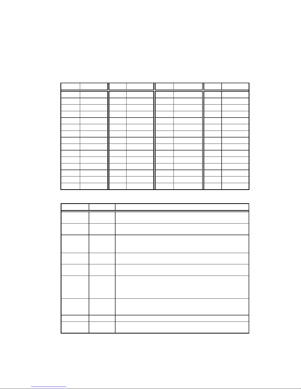
Number Signal name Number Signal name Number Signal name Number Signal name
1 +5V 2 +5V 31 GND 32 GND
3 D0 4 D1 33 A8 34 A9
5 D2 6 D3 35 A10 36 A11
7 D4 8 D5 37 A12 38 A13
9 D6 10 D7 39 A14 40 A15
11 GND 12 GND 41 +5V 42 +5V
13 D8 14 D9 43 A16 44 A17
15 D10 16 D11 45 A18 46 A19
17 D12 18 D13 47 BHE- 48 GND
19 D14 20 D15 49 GND 50 RD21 +5V 22 +5V 51 WR- 52 RESET23 A0 24 A1 53 GND 54 GND
25 A2 26 A3 55 READY 56 INT27 A4 28 A5 57 GND 58 GND
29 A6 30 A7 59 CPUCLK 60 GND
JEXT Connector Pin Arrangement
Signal name Input/output Function
A[0..19] Output Address bus signal, which is originally the CPU address signal received
at a buffer.
BHE- Output Byte high enable signal, which is originally the CPU UBE- signal
received at a buffer.
D[0..15] Input/ output Data bus signal, which is originally the CPU data bus signal received at
a buffer.
It is pulled up with a 10 kΩ resistor on the board.
RD- Output Read cycle timing signal, which becomes active only when the JEXT
space is accessed.
WR- Output Write cycle timing signal, which becomes active only when the JEXT
space is accessed.
READY Input Signal indicating the end of a cycle. It is valid only for the JEXT space.
To have the CPU recognize READY securely, it is necessary to keep
READY active until RD- or WR- becomes inactive. It is pulled up with
a 10 kΩ resistor on the board.
INT- Input Active-low interrupt request signal, which is connected to the
P23/INTP02 pin of the CPU via a buffer and the NMI pin of the CPU via
a mask logic. It is pulled up with a 10 kΩ resistor on the board.
RESET- Output Active-low system reset signal
CLK Output Clock signal, which is connected to the CLKOUT pin of the V852 via a
buffer.
JEXT Connector Signals
Page 41

RTE-V852-PC USER’ S MANUAL (Rev. 1.10)
40
RD-
A[0..19]
BHE-
T1
T2
Write cycle
Read cycle
READY
D[0..15]
WR-
T9T8Dout
High
T7
Din
RD-
A[0..19]
BHE-
T10
T12
T15
READY
D[0..15]
WR-
T17
T16
T18
T6
High
T14T3T4
T11
T13
T5
JEXT Bus Cycle
Symbol Description Min. (ns) Max. (ns)
T1 RD address setup time 0
T2 RD address hold-up time 0
T3 RD cycle time 50
T4 RD cycle interval 20
T5 RD data setup time 15
T6 RD data hold time 0
T7 RD READY WAIT setup time 0
T8 RD READY setup time 0
T9 RD READY hold time 0
T10 WR address setup time 0
T11 WR address hold time 20
T12 WR cycle time 50
T13 WR cycle interval 20
T14 WR data delay time 20
T15 WR data hold time 20
T16 WR READY WAIT setup time 0
T17 WR READY setup time 0
T18 WR READY hold time 0
JEXT Bus AC Specifications
2134567820191817161514131211109222123242526272840393837363534333231302941434445464748605958575655545352515049
41
JEXT Pin Arrangement
Page 42

RTE-V852-PC USER’ S MANUAL (Rev. 1.10)
41
9. OTHER CPU RESOURCES
9.1. RESET-
The factors listed below trigger a CPU reset. These factors reset the CPU. They also system-reset
the board control circuit.
• Power-on reset: Occurs when the power to the board is switched on.
• Reset request received from JROMEM: Input to the RESET- pin of the JROMEM connector
on the Base board. See Section 3.19 for details.
• Reset by the SWRESET: Generated by the reset switch (SWRESET) on the rear panel of the
base board.
• Reset by RESET_SW: Generated by pressing the reset switch (RESET_SW) on the Socket
board.
• Reset request from the host: Sent via the ISA bus.
The figure below outlines the reset signal generation logic.
ISA_ResetRequest
To CPU
SW_RESET
JROM_EM
RESET-
RESET-
RESET
Socket-BoardBase-Board
RESET_SW
J8-5Pin
9.2. NMI-
An NMI to the CPU occurs as follows:
• Request received from controller on the Base board: An NMI can be generated by an
interrupt request received from the UART/PRINT controller (TL16C552A) on the Base board (see
Section 6.2).
An NMI can also be generated based on the interrupt request received from the timer (µPD71054)
on the Base board (see Section 6.3). This interrupt is used by the Multi debugger functions such
as the profiler function (see Section 6.11).
Which of the above interrupt requests is to be connected to the NMI can be controlled by
programming (see Section 6.8).
• Request based on Ready time-over: Time-out Ready occurs when a bus cycle has not been
completed within a certain period. It is possible to generate an NMI request upon the occurrence
of the time-out ready status (see Section 6.8).
• Request received from JEXT bus: NMI can be generated when the INT signal of the JEXT bus
goes active (see Section 6.8).
Page 43

RTE-V852-PC USER’ S MANUAL (Rev. 1.10)
42
• NMI request from JROMEM: NMI is generated by the input to the NMI pin of the JROMEM
connector on the Base board. See Section 3.19 for details.
• Request received from ISA bus: NMI can be used for controlling communications via the ISA
bus. This NMI is used when the Multi debugger is connected through the ISA bus.
• Request by NMI_SW: NMI is generated when the NMI switch (NMI_SW) on the Socket board is
pressed.
It is possible to mask the NMI by means of hardware. See Sections 6.8 and 6.10 for an explanation
of the masking method.
The following procedure must be applied when an NMI occurs.
À Mask the NMI by means of hardware by setting NMIMASK of the NMI mask port to “ 1” .
Á Determine the NMI request source. This can be identified at the NMI status port (see Section
6.9).
 Clear the request by performing NMI processing for the request source.
à Reset the mask by setting NMIMASK of the NMI mask port to “ 0” .
Ä Return from NMI processing.
The figure below outlines the NMI generation logic.
UART1_NMIEN
To CPU
NMI-
BASE_NMI-
NMI_MASK
From SW_NMI
From JROM_EM
SW_NMI-
ROM_EMLT_NMI-
UART1_NMI
UART2_NMIEN
UART2_NMI
PRT_NMIEN
PRT_NMI
ISACOM_NMIEN
ISACOM_NMI
EXTBUS_NMIE
EXTBUS_NMI
TOVER_NMIEN
TOVER_NMI
TIMER_NMIEN
TIMER_NMI
Page 44

RTE-V852-PC USER’ S MANUAL (Rev. 1.10)
43
9.3. MASKABLE INTERRUPTS (INT0(P22/INTP01), INT1 (P24/INTP03))
The factors listed below trigger INT0 (P00/INTP00). See Section 6.12 for details of selecting an
interrupt.
• Request from controller on the Base board: INT0 (P22/INTP01) can be generated by the
UART-CH#1 or PRINTER interrupt request received from the UART/PRINT controller
(TL16C552A) on the Base board (see Section 6.2).
• Request from ISA bus: INT0 (P22/INTP01) can be used for controlling communications via the
ISA bus.
The factors listed below trigger INT1 (P24/INTP03). See Section 6.13 for details of selecting an
interrupt.
• Request received from controller on the Base board: INT1 (P24/INTP03) can be generated
by an interrupt request received from the timer (µPD71054) on the Base board (see Sections 6.3
and 6.11).
• Request based on Ready time-over: Time-out Ready occurs when a bus cycle has not been
completed within a certain period. It is possible to generate INT1 (P24/INTP03) upon the
occurrence of the time-out ready signal (see Section 6.11).
It is possible to mask INT0/INT1 by means of hardware. See Section 6.10 for an explanation of the
masking method.
The following procedure must be applied when an INT0/INT1 occurs.
À Mask the INT0/INT1, by means of hardware, by setting INT0MASK or INT1MASK of the
NMI/INT0/INT1 mask port to “ 1” .
Á Determine the INT0/INT1 request source. This can be identified at the INT0 or INT1 status port
(see Sections 6.14 and 6.15).
 Clear the request by performing interrupt processing for the request source.
à Reset the mask by setting INT0MASK or INT1MASK of the NMI/INT0/INT1 mask port to “ 0” .
Ä Return from NMI processing.
Page 45

RTE-V852-PC USER’ S MANUAL (Rev. 1.10)
44
The figure below outlines the INT0/INT1 generation logic.
UART1_INT0EN
To CPU
P22/INTP01
SW3-2
INT0_MASK
UART1_INT0
TOVER_INT1
TOVER_INT1
TIMER_INT1
TIMER_INT1
ISACOM_INT0EN
ISACOM_INT0
PRT_INT0EN
PRT_INT0
To CPU
P24/INTP03
SW3-4
INT1_MASK
9.4. PORT
Among the CPU ports, P4[0..7], P5[0..7], P6[0..3] and P9[0..6], which are related to the external
extension bus, are used for connection to the Base board.
Other ports including P0[0..7], P1[0..7], P2[0..7], P3[0..7], and P10[0..3] are connected to the
connectors on the Socket board. They can be used as desired by the user. See Section 3.5 for
details the pin arrangements of the connectors and Chapter 13 for details of the connections on the
board.
Page 46

RTE-V852-PC USER’ S MANUAL (Rev. 1.10)
45
10. Multi MONITOR
The ROM chip on the board is incorporated with the Multi monitor. The following cautions should be
observed when the board is connected to the Multi server as the host.
10.1. MONITOR WORK RAM
The monitor uses the first 32-KB (1F-8000H to 1F-EFFFH) area in the SRAM as work RAM. In other
words, user programs are not allowed to use logical addresses xF-8000H to xF-EFFFH (x: 0 to 1).
(See Section 5.1.)
10.2. INTERRUPTS
When running on the Multi monitor, user programs cannot use interrupts at present.
10.3. _INIT_SP SETTING
_INIT_SP (stack pointer initial value) is set to 1F-7FFCH (immediately before the monitor work RAM)
by the monitor. (_INIT_SP can be changed in the Multi environment.)
10.4. REMOTE CONNECTION
Either serial or ISA bus connection can be selected for operation with the Multi server. To switch
from serial connection to ISA bus connection or vice versa, it is necessary to reset the monitor (by
pressing the reset switch on the rear panel) and run the Check RTE utility of RTE for Windows.
10.5. TIMER INTERRUPT
The profiler function of the Multi debugger cannot be used if timer interrupt is inhibited (see Section
4.1 for details of timer interrupt setting).
The characteristics of the CPU used with the V852 make it necessary to use a timer interrupt for the
break point function. Therefore, the Multi debugger cannot be used if timer interrupt is inhibited.
Page 47

RTE-V852-PC USER’ S MANUAL (Rev. 1.10)
46
11. RTE COMMANDS
When the monitor and server (rteserv) are connected, the TARGET window is opened. The RTE
commands can be issued in this window. The following table lists the RTE commands.
Command Description
HELP or ? Displays help messages.
INIT Initializes.
VER Displays the version number.
SFR Changes or displays the internal register (SFR).
RTE Commands
Some commands require parameters. All numeric parameters such as addresses and data are
assumed to be hexadecimal numbers. The following numeric representations are invalid:
0x1234 1234H $1234
11.1. HELP (?)
<Format> HELP [command-name]
Displays a list of RTE commands and their formats. A question mark (?) can also be used in place
of the character string HELP. If no command name is specified in the parameter part, the HELP
command lists all usable commands.
<Example> HELP SFR
Displays help messages for the SFR command.
11.2. INIT
<Format> INIT
Initializes the RTE environment. Usually, this command should not be used.
11.3. VER
<Format> VER
Displays the version number of the current RTE environment.
11.4. SFR
<Format> SFR[register-name[data]]
Displays the data in the CPU’ s internal register (SFR) or writes data into it.
When the parameters are omitted, this command displays a list of register names which can be
specified with the SFR command.
When only the register-name parameter is specified, this command reads and displays the data in the
specified register.
When both the register-name and data parameters are specified, this command writes the data into
the specified register.
Specifying a display command for a read-inhibited register or a write command for a write-inhibited
register results in an error. The access size for read or write is automatically set to the same size as
that of the register.
Page 48

RTE-V852-PC USER’ S MANUAL (Rev. 1.10)
47
12. APPENDIX BUS CYCLE
12.1. TIME-OVER READY
On the Base board, when an external bus cycle generated by the CPU has not been completed within
a certain period, the time-over ready status is generated to forcibly complete the cycle. Time-over
ready is generated when a bus cycle has been generated continuously for 1024 clocks (approx. 30.7
µs when operating at 33 MHz).
When time-over ready occurs, the TOVER LED on the Base board lights and the NMI and INT1
(P24/INTP03) interrupt factor is generated. The TOVER LED goes out, and the NMI and INT1
(P24/INTP03) interrupt factor can be cleared by writing to the NMI/INT1 request clear port.
See Sections 3.18, 6.8, 6.11 and 6.13 for details.
12.2. DRAM INTERFACE
12.2.1. Outline
DRAM access supports both normal mode and page mode.
In page mode, the RAS signal issued to the DRAM is held active as long as access to the same row
address continues and access is performed by controlling only the CAS signal. This makes it
possible to reduce the access time for continuous access to the same row address. If, however, an
access to another row address is generated, the access time becomes slower when continuous
access fails because the RAS signal is deactivated after the start of the cycle and access is started
only after the completion of RAS precharge.
Therefore, whether normal or page mode can provide the better performance depends on the number
of times continuous access to DRAM occurs.
Normal or page mode can be set by programming (see Section 6.7).
12.2.2. Signal Description
The signals used for waveforms described in this chapter are defined as follows:
CLKOUT: System clock output by the CPU.
ASTB: External address strobe signal output by the CPU.
DSTB-: External data strobe signal output by the CPU.
WAIT-: Wait signal input to the CPU.
HIT: Signal that indicates whether a row address is the same as one used in the previous cycle,
because the DRAM is used in the page mode. This signal is generated by the DRAM
control circuit.
RAS-: RAS signal input to the DRAM.
CASn-: CAS signal input to the DRAM. One CAS- signal is provided for each byte in the word
(hence, CAS0- to CAS3-).
WE-: WE signal input to the DRAM.
Page 49
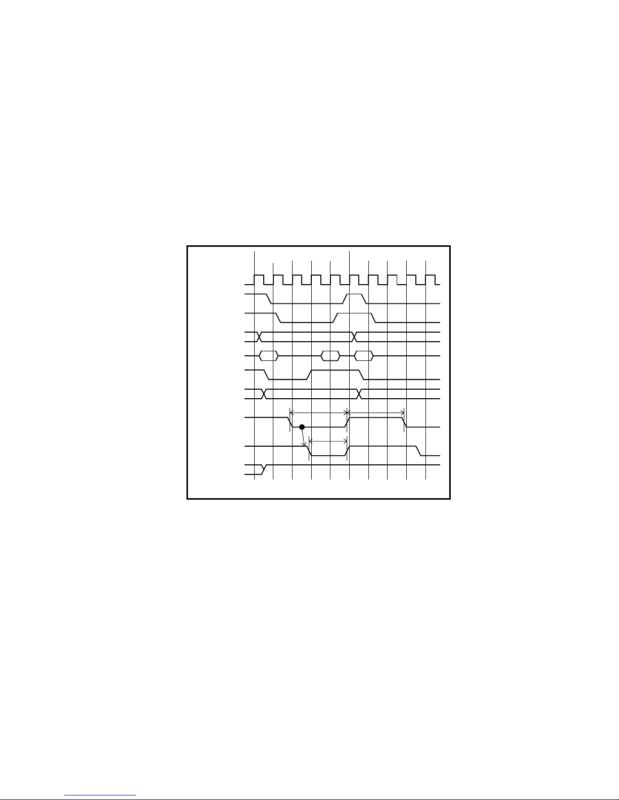
RTE-V852-PC USER’ S MANUAL (Rev. 1.10)
48
12.2.3. Single Read (Normal Mode)
In normal mode, read cycles always occur as single read cycles, as shown in the following timing
chart.
• In this timing chart, two read cycles are generated successively after the completion of RAS
precharge of the previous cycle. The second of these cycles is kept waiting during RAS
precharging.
• Xclk, Yclk and Zclk represent, respectively, the clock counts for the “ RAS precharge time,”
“ RAS Low width,” and “ CAS Low width in read access” which are set in the program (see
Section 6.7).
• When the “ RAS minimum low width” setting is larger, by two or more, than the “ CAS Low
width in read access,” Zclk becomes equal to (Yclk - 1).
WE-
CASn-
Zclk
XclkYclk
HIT
RAS-
Sig1: A16 to A19,UBEN-,LBEN-,R/W-
Sig1
DATA
ADDRADDR
AD0 to AD15
WAIT-
ASTB
TWTWT2T1T3TWTWT2T1
CLKOUT
DSTB-
Page 50

RTE-V852-PC USER’ S MANUAL (Rev. 1.10)
49
12.2.4. Single Write (Normal Mode)
In normal mode, write cycles always occur as single write cycles, as shown in the following timing
chart.
• In this timing chart, two write cycles are generated successively after the completion of RAS
precharge of the previous cycle. The second of these cycles is kept waiting during RAS
precharging.
• Xclk and Yclk represent, respectively, the clock counts for the “ RAS precharge time” and
“ RAS Low width,” which are set in the program (see Section 6.7).
The “ CAS Low width in write access” is always one clock.
• When the “ RAS minimum low width” setting is two clocks or larger, the “ CAS Low width in
write access” becomes equal to (Yclk - 1).
WE-
CASn-
XclkYclk
HIT
RAS-
Sig1: A16 to A19,UBEN-,LBEN-,R/W-
Sig1
DATA
ADDRADDR
AD0 to AD15
WAIT-
ASTB
TWTWT2T1T3TWTWT2T1
CLKOUT
DSTB-
DAT
A
Page 51
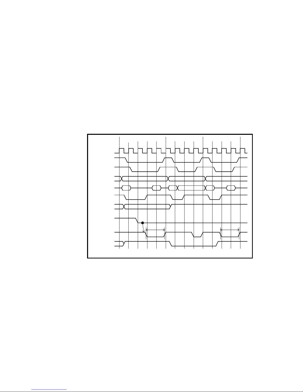
RTE-V852-PC USER’ S MANUAL (Rev. 1.10)
50
12.2.5. Page Access (Page Mode, Same Row Address)
In the page mode cycle, continuous access to the same row address is performed by controlling only
the CAS signal while keeping the RAS signal active, as shown in the following timing chart.
• In this timing chart, those cycles which access the same row address are generated in the
order of read, write then read, after the completion of RAS precharge of the previous cycle.
• Zclk represents the clock count for the “ CAS Low width in read access” (see Section 6.7).
The “ CAS Low width in write access” is always one clock.
• W hen the “ RAS minimum low width” (Yclk) setting is larger, by two or more, than the
“ CAS Low width in read access,” Zclk of the first cycle of the access of the same row
address becomes equal to (Yclk - 1).
• Accessing the same row address in page mode allows the access time to be increased by at
least one wait state compared to when page mode is not used. The access speed can be
further increased if the clock count for the “ RAS precharge time” is more than two clocks.
WE-
CASn-
HIT
RAS-
Sig1: A16 to A19,UBEN-,LBEN-,R/W-
Sig1
DATADATA ADDR ADDRADDR
AD0 to AD15
WAIT-
ASTB
T3T2T1T3T2T1
CLKOUT
DSTB-
Zclk
T1 T2TW TW TW TW T3
DATA
Read CycleWrite CycleRead Cycle
Zclk
Page 52
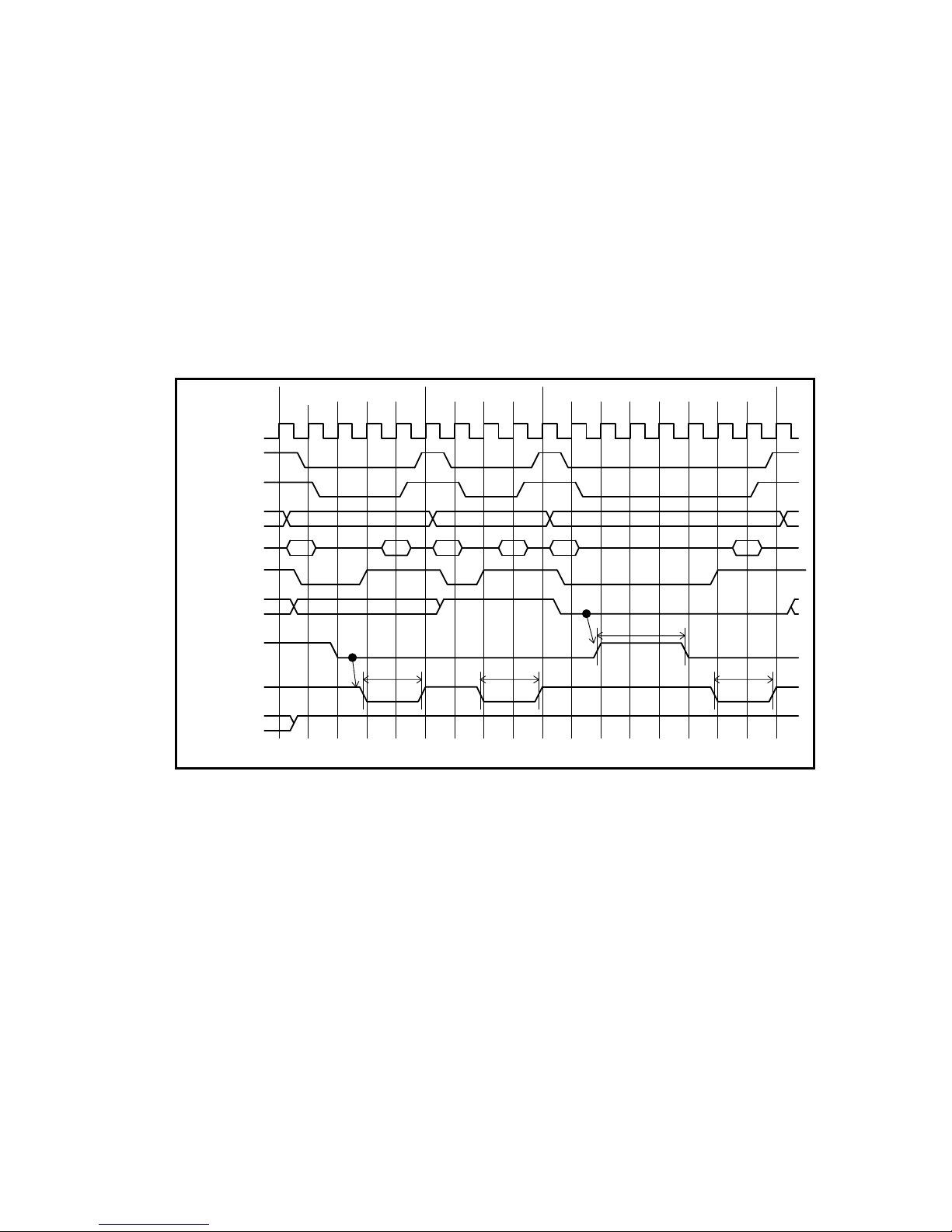
RTE-V852-PC USER’ S MANUAL (Rev. 1.10)
51
12.2.6. Page Access (Page Mode, Different Row Addresses)
When a different row address from the previously-accessed row address is accessed in page mode,
the RAS signal is deactivated from the start of the cycle and activated again after having waited for a
period equal to the RAS signal precharge time, as shown in the following timing chart.
• In this timing chart, two ready cycles for the same row address occur after the completion of
RAS precharge of the previous cycle, then a ready cycle for a different row address occurs.
• Xclk and Zclk represent, respectively, the clock counts for the “ RAS precharge time” and
“ CAS Low width in read access,” which are set in the program (see Section 6.7).
• When the “ RAS minimum low width” (Yclk) setting is larger, by two or more, than the
“ CAS Low width in read access,” Zclk of the first cycle of the accesses to the same row
address becomes equal to (Yclk - 1).
WE-
CASn-
HIT
RAS-
Sig1: A16 to A19,UBEN-,LBEN-,R/W-
Sig1
DATA
ADDRADDR
ADDR
AD0 to AD15
WAIT-
ASTB
T3 TWTWTWTWTWTWT2T1T3TWTWT2T1
CLKOUT
DSTB-
Zclk
T1 T2 T3
DATA
Read CycleRead CycleRead Cycle
ZclkZclk
Xclk
DATA
Page 53
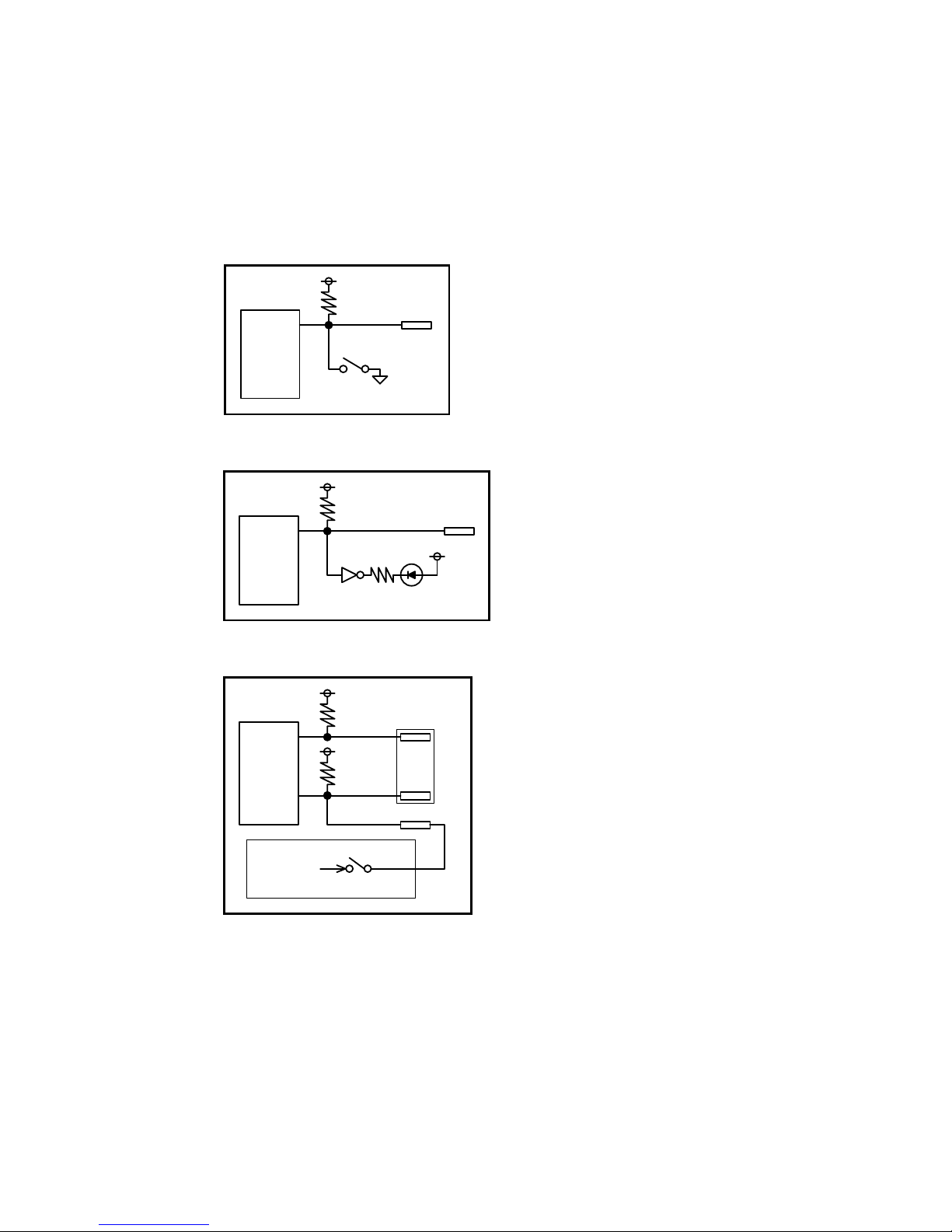
RTE-V852-PC USER’ S MANUAL (Rev. 1.10)
52
13. APPENDIX CPU PORT CONNECTIONS
This chapter describes the connection schemes of the CPU ports which are connected to the
connectors on the Socket board.
13.1. P00 TO P07
P0[0:7]
SW2
JPORT0
47 k
Ω
CPU
13.2. P10 TO P17
P1[0:7]
74ACT540
JPORT1
CPU
47 k
Ω
13.3. P20 TO P27
P2[5:7]
JPORT2
47 k
Ω
CPU
P2[1:4]
J5/6
Base Board
Interrupt
SW3
47 k
Ω
J1/2
Page 54
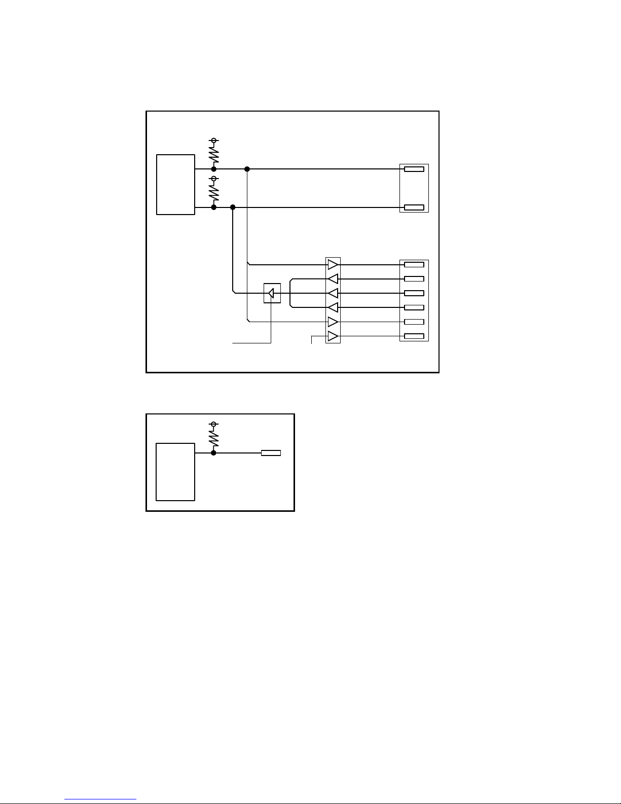
RTE-V852-PC USER’ S MANUAL (Rev. 1.10)
53
13.4. P30 TO P37
P3[4,6,7]
J3
CPU
TxDP22
232C
Driver
Buf.
47 k
Ω
RxDP34
P36
P37
CTS
DSR
P35 RTS
P27 DTR
P3[5]
P3[1,2,3]
47 k
Ω
JPORT3
P3MODE
GND
13.5. P100 TO P103
P10[0:3]
47 k
Ω
JPRT10
CPU
Page 55

RTE-V852-PC USER’ S MANUAL (Rev. 1.10)
54
- Memo -
RTE-V852-PC User’ s Manual M662MNL02
Created on August 15, 1996. Rev. 1.00
Midas lab
 Loading...