

Page 1

RTE-V821-PC
User's Manual
Midas lab
Page 2

RTE-V821-PC USER’ S MANUAL
1
REVISION HISTORY
Date of
enforcement
Revision Page Description
August 11, 1995 1.0 First issue
December 25, 1995 1.1 11, 12 Correction of error related to descriptions about SW2
(1-2 and 3-4) settings
Page 3

RTE-V821-PC USER’ S MANUAL
2
CONTENTS
1. INTRODUCTION..........................................................................................................................4
1.1. NUMERIC NOTATION ........................................................................................................... 4
2. FEATURES AND FUNCTIONS.....................................................................................................5
3. BOARD CONFIGURATION..........................................................................................................6
3.1. RESET SWITCH (SWRESET)...............................................................................................6
3.2. POWER SUPPLY CONNECTOR (JPOWER).........................................................................6
3.3. SWITCH1 (SW1) ..................................................................................................................6
3.4. SWITCH2 (SW2) ..................................................................................................................7
3.5. LED ......................................................................................................................................7
3.6. TEST PINS (TP) .................................................................................................................... 7
3.7. SUBPORT (JSUBPORT).......................................................................................................7
3.8. SERIAL CONNECTOR (JSIO)...............................................................................................8
3.9. CPU TEST PINS (JCPU).......................................................................................................9
3.10. CLOCK SOCKET (OSC1)......................................................................................................9
3.11. DRAM-SIMM SOCKETS......................................................................................................10
3.12. ROM SOCKETS.................................................................................................................. 10
4. INSTALLATION AND USE.......................................................................................................... 11
4.1. BOARD SETTING............................................................................................................... 11
4.2. INSTALLATION ON THE ISA BUS.......................................................................................12
4.3. STANDALONE USE OF THE BOARD .................................................................................12
5. HARDWARE REFERENCES...................................................................................................... 13
5.1. MEMORY MAP....................................................................................................................13
5.2. I/O MAP..............................................................................................................................14
5.2.1. Port Unit (PORT)..........................................................................................................14
5.2.2. Wait Control Unit (WCU).............................................................................................. 14
5.2.3. DRAM Control Unit (DRAMC)....................................................................................... 15
5.2.4. ROM Controller (ROMC)...............................................................................................15
5.2.5. DMA Controller (DMAC)................................................................................................ 15
5.2.6. Realtime Pulse Unit (RPU) ...........................................................................................15
5.2.7. Serial Control Unit (SCU).............................................................................................. 15
5.2.8. Interrupt Control Unit (ICU)...........................................................................................16
5.2.9. Bus Arbitration Unit (BAU)............................................................................................ 16
5.2.10. Clock Generator (CG)............................................................................................... 16
5.2.11. Watchdog Timer Unit (WDT) ........................................................................................16
6. SYSTEM-I/O..............................................................................................................................17
6.1. UART/TIMER (SCC2691)....................................................................................................17
6.2. PIO (µPD71055)..................................................................................................................17
7. JEXT BUS SPECIFICATION.......................................................................................................19
8. OTHER CPU RESOURCES.......................................................................................................21
Page 4

RTE-V821-PC USER’ S MANUAL
3
8.1. RESET-...............................................................................................................................21
8.2. NMI-....................................................................................................................................21
9. Multi MONITOR .........................................................................................................................22
9.1. MONITOR WORK RAM ......................................................................................................22
9.2. INTERRUPTS..................................................................................................................... 22
9.3. _INIT_SP SETTING ............................................................................................................22
9.4. REMOTE CONNECTION.................................................................................................... 22
10. RTE COMMANDS......................................................................................................................23
10.1. HELP (?).............................................................................................................................23
10.2. INIT.....................................................................................................................................23
10.3. VER....................................................................................................................................23
10.4. INB, INH, AND INW.............................................................................................................23
10.5. OUTB, OUTH, AND OUTW................................................................................................. 24
10.6. SFR.................................................................................................................................... 24
11. APPENDIX.................................................................................................................................25
11.1. CPU PINS...........................................................................................................................25
Page 5
RTE-V821-PC USER’ S MANUAL
4
1. INTRODUCTION
This manual describes the RTE-V821-PC, which is an evaluation board for the V821, NEC's
CPU. With the RTE-V821-PC, it is possible to develop and debug programs, and evaluate the
CPU performance, using the GreenHills Multi debugger. Communication with this debugger is
carried out using the IBM-PC/AT ISA bus or RS-232C serial interface. It is also possible to
expand memory and I/O units using local bus connectors provided on the evaluation board.
1.1. NUMERIC NOTATION
This manual represents numbers according to the notation described in the following table.
Hexadecimal and binary numbers are hyphenated at every four digits, if they are difficult to read
because of many digits being in each number.
Number Notation rule Example
Decimal
number
Only numerals are indicated. "10" represents number 10 in decimal.
Hexadecimal
number
A number is suffixed with letter H. "10H" represents number 16 in decimal.
Binary
number
A number is suffixed with letter B. "10B" represents number 2 in decimal.
Number Notation Rules
Page 6
RTE-V821-PC USER’ S MANUAL
5
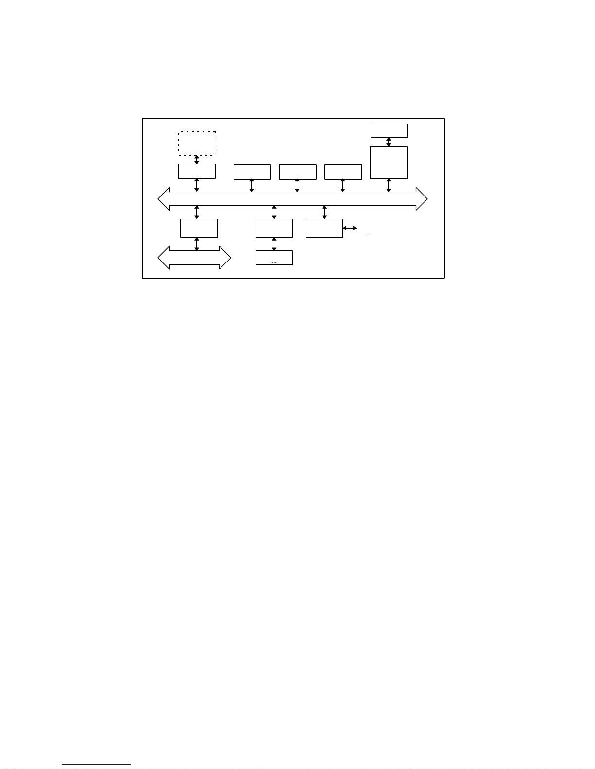
2. FEATURES AND FUNCTIONS
The overview of each function block of the RTE-V821-PC is shown below.
V82
1
JSUBPOR
T
CONNECTOR
ISA Bus
Local Bus
ISA BUS I/F
JEX
T
CONNECTOR
D-RAMS-RAMROM
TIMER/SIO
Interna
l
Control
RS-232C
CONNECTOR
PIO
USER
HW
RTE-V821-PC Block Diagram
Features
• ROM: 128 Kbytes (64K x 16 bits)
• SRAM: 128 Kbytes (64K x 16 bits)
• DRAM: 4, 8, or 16 Mbytes (standard of 4 Mbytes) installed in a 72-pin SIMM socket
• RS-232C port (9-pin D-SUB connector)
• Communication function supported using the ISA bus of a PC/AT or compatible
• Local bus connector for user-installed expansion equipment
• Connector which outputs synchronous serial signals of the CPU and some port signals
• Processor pin connector enabling measurement of all CPU signals
• External reset switch provided on the rear panel
• Connection pins for ROM in-circuit debugger
Page 7
RTE-V821-PC USER’ S MANUAL
6
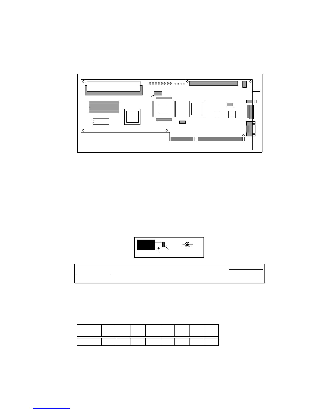
3. BOARD CONFIGURATION
The physical layout of the major components on the RTE-V821-PC board is shown below. This
chapter explains each component.
RTE-V821-PC Board Top View
3.1. RESET SWITCH (SWRESET)
SWRESET is a reset switch. Pressing this switch causes the CPU to be reset.
3.2. POWER SUPPLY CONNECTOR (JPOWER)
When this board is to be used as a standalone, that is, without being inserted in an ISA bus slot,
the board should be supplied with power from an external power supply by connecting it to the
JPOWER connector.
The external power should be one rated as listed below.
Voltage: 5 V
Current: Maximum of 1 A (excluding the current supplied to the JEXT connector)
Mating connector: Type A (5.5 mm in diameter)
Polarity:
GND
GND
+5V
+5V
[Caution] When attaching an external power supply to the board, be careful about its
connector polarity. When inserting the board into the ISA bus slot, do not attach the JPOWER
connector to an external power supply.
3.3. SWITCH1 (SW1)
SW1 is a switch for selecting the I/O address of the ISA bus. Switch contacts 1 to 8
corresponds to ISA addresses A4 to A11, respectively (A12 to A15 are fixed at 0). This means
that the I/O address that can be selected ranges between 000xH and 0FFxH. When a switch
contact is open, it corresponds to 1. When it is closed, it corresponds to 0.
SW1
contact
1 2 3 4 5 6 7 8
Address A4 A5 A6 A7 A8 A9 A10 A11
SW1-to-ISA Address Correspondence
SW2
POWER
CS0
CS1
CS2
CS3
TOVER
P06
P07
SCC/
TIMER
LED TP
DRAM SIMM
JCPU
SWRESET
JPOWER
JEXT
V821
JSIO
JSUBPORT
SRAM
SW1
ROM
PLD
PLD
NMI-
RD_WRALL-
RESET-
GND
PIO
OSC1
Page 8
RTE-V821-PC USER’ S MANUAL
7
3.4. SWITCH2 (SW2)
SW2 is a switch for general-purpose input ports. When a switch contact is open, it
corresponds to 1. When it is closed, it corresponds to 0. See Section 6.1.2 for details.
3.5. LED
The LEDs are used to indicate statuses, as listed below.
LED Description
CS0 Lights when the CS0 pin of the CPU is active (low).
CS1 Lights when the CS1 pin of the CPU is active (low).
CS2 Lights when the CS2 pin of the CPU is active (low).
CS3 Lights when the CS3 pin of the CPU is active (low).
TOVER Lights when a time-out occurs.
P06 PIO: PORT0-6
P07 PIO: PORT0-7
LED Indication
3.6. TEST PINS (TP)
Test pins are used to connect a ROM in-circuit debugger. Some of them accept control
signals from the ROM in-circuit debugger, and the others output trace timing signals. The
following table lists the signal name and function related to each test pin.
Signal Input/
output
Function
RESET- Input When a low level is supplied to this test pin, the CPU is reset. A
reset request signal from the ROM in-circuit debugger is
connected to the test pin. The test pin is pulled up with 1kΩ.
NMI- Input When a low level is supplied to this test pin, an NMI signal is
given to the CPU. This signal can be masked by software. An
NMI request (break request) signal from the ROM in-circuit
debugger is connected to the test pin. The test pin is pulled up
with 1kΩ.
RD_WR_ALL- Output This signal is obtained by ORing (negative logic) the CPU's
UMWR-, LMWR-, MRD-, IOWR-, and IORD- signals. It is used
as a trace timing signal by the ROM in-circuit debugger.
GND ------- This test pin is at a ground level. The ground level of the ROM
in-circuit debugger is connected to the test pin.
Test Pin Functions
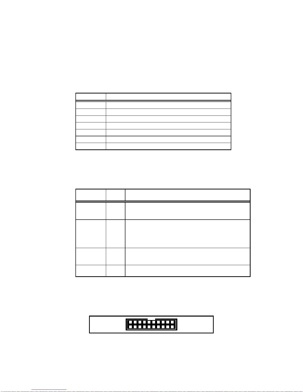
3.7. SUBPORT (JSUBPORT)
The JSUBPORT connector makes some CPU pins accessible to the outside. Its pin
arrangement is shown below. The pins of the JSUBPORT connector are defined in the
following table.
213456782019181716151413121110
9
JSUBPORT Pin Arrangement
Page 9
RTE-V821-PC USER’ S MANUAL
8
Number Signal Description
1,3,5,7,9,
11,13,15
GND
2 SCLK-/P07 Connected directly to the CPU and pulled up with 47 kΩ.
4 SI/P05 Connected directly to the CPU and pulled up with 47 kΩ.
6 SO/P06 Connected directly to the CPU and pulled up with 47 kΩ.
8 INTP00-/TO00 Connected directly to the CPU and pulled up with 10 kΩ.
10 INTP02-/TO01 Connected directly to the CPU and pulled up with 10 kΩ.
12 TCLR/P00 Connected directly to the CPU and pulled down with 47 kΩ.
14 INTP13-/TI Connected directly to the CPU and pulled up with 10 kΩ.
16 DREQ0/P01 Connected directly to the CPU and pulled up with 47 kΩ.
17 DACK0-/P02 Connected directly to the CPU and pulled up with 47 kΩ.
18 DREQ1/P03 Connected directly to the CPU and pulled up with 47 kΩ.
19 DACK1-/P04 Connected directly to the CPU and pulled up with 47 kΩ.
20 NC Not connected
JSUBPORT Connector Signals
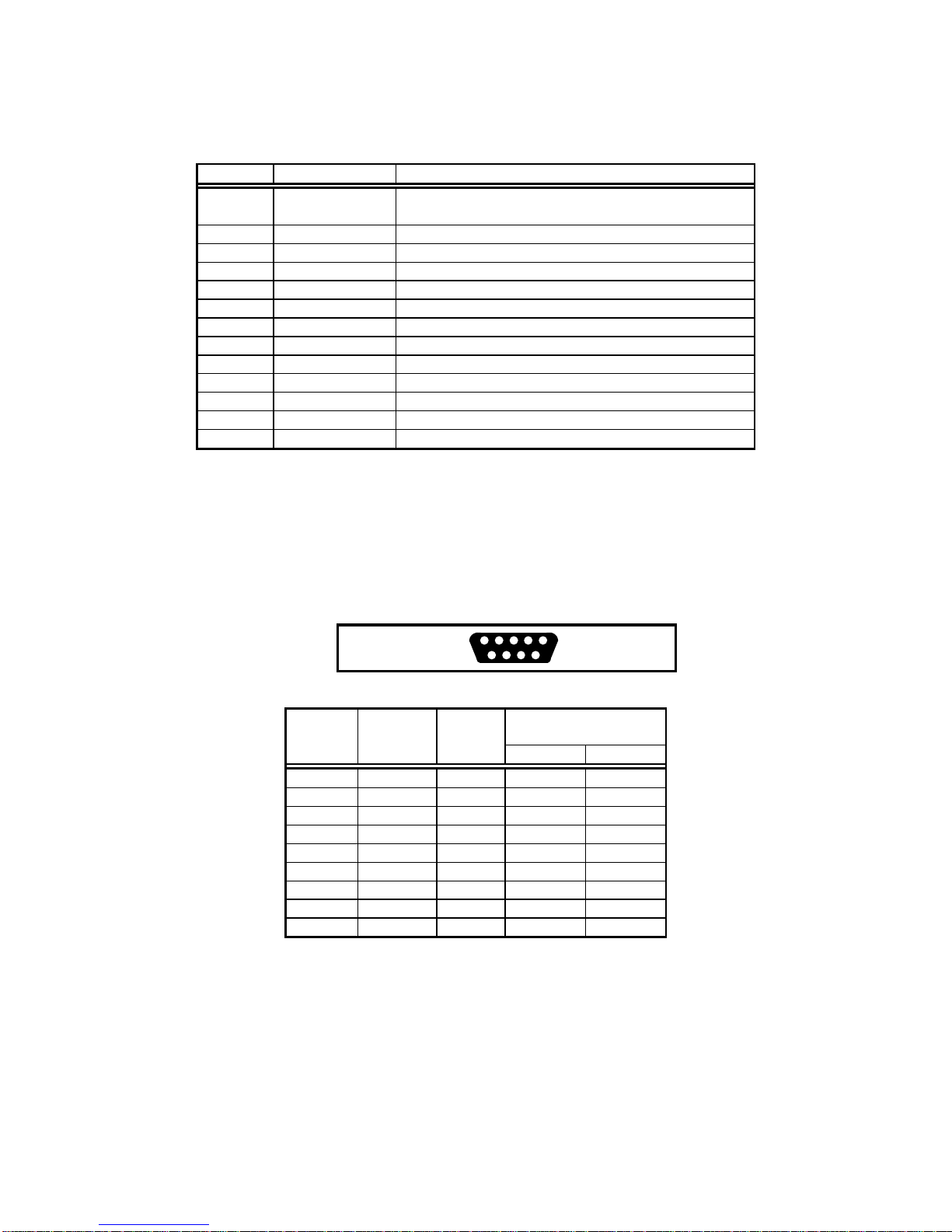
3.8. SERIAL CONNECTOR (JSIO)
JSIO is a connector for the RS-232C interface controlled by the serial controller (SCC2691). It
is a 9-pin D-SUB connector (D-SUB9) generally used with the PC/AT. All signals at this
connector are at RS-232C level. Its pin arrangement and signal assignment are shown and
listed below.
For connection signals connected to the host computer, the table gives the wirings for both the
D-SUB9 pins and D-SUB25 pins on the host side. (These are general cross-cable wirings.)
198765432
JSIO Pin Arrangement
JSIO pin Signal name Input/
output
Connector pin number on
the host side
D-SUB9 D-SUB25
1 NC
2 RxD(RD) Input 3 2
3 TxD(SD) Output 2 3
4 DTR(DR) Output 1, 6 6, 8
5 GND 5 7
6 DSR(ER) Input 4 20
7 RTS(RS) Output 8 5
8 CTS(CS) Input 7 4
9 NC
JSIO Connector Signals
Page 10

RTE-V821-PC USER’ S MANUAL
9
3.9. CPU TEST PINS (JCPU)
The JCPU connector pins are connected to the corresponding CPU pins. The connector pin
numbers correspond to the CPU pin numbers on a one-to-one basis. The connector pins can
be used to handle CPU signals for circuit expansion or test purposes.
3.10. CLOCK SOCKET (OSC1)
The OSC1 socket is connected to an oscillator or crystal used to supply clock pulses to the CPU.
The V821 can use a PLL for system clock generation. The PLL mode is selected according to
the state of the TCLR/P00 pin at a reset. The TCLR/P00 pin is pulled down with 47 kΩ in the
RTE-V821-PC, so the PLL mode is usually selected. In this case, the frequency of the
oscillator or crystal connected to the OSC1 socket is one-fifth the system clock frequency.
When the TCLR/P00 pin is high, the frequency of the oscillator or crystal is twice the system
clock frequency.
The OSC1 socket accepts a 14-, 8-, or 3-pin oscillator, or a crystal. The oscillator and crystal
should be mounted as shown below. Capacitors must be used together with the crystal.
3-pin oscillator
8-pin oscillator
14-pin oscillator
1PIN
1PIN
1PIN
How to Mount Oscillators
Capacitor
Crystal
Capacitor
1PIN
How to Mount a Crystal
[Caution] When a crystal is used, oscillation may become unstable and inoperable. It is
recommended that an oscillator be used.
Page 11

RTE-V821-PC USER’ S MANUAL
10
[Caution] When you have to cut an oscillator or crystal pin for convenience, be careful not to
cut it too short, or otherwise the frame (housing) of the oscillator crystal may touch a pin in the
socket, resulting in a short-circuit occurring.
[Note] When the clock frequency is changed, it is necessary to review the refresh interval of
the DRAM. The system clock is factory-set to a range of 12 to 25 MHz by the ROM initialization
routine.
3.11. DRAM-SIMM SOCKETS
The RTE-V821-PC has DRAM-SIMM socket used to install 4 Mbytes (standard) of SIMM.
Each socket can hold a 72-pin 4-, 8-, or 16-Mbyte SIMM (known as a module for DOS/V
machines), so it is easy to expand the capacity of DRAM. When the system clock frequency is
25 MHz, use DRAM chips having an access time of 60 ns or less.
The capacity of installed SIMMs can be detected using a PIO port. (See Section 6.1.2.)
3.12. ROM SOCKETS
The RTE-V821-PC has a ROM socket, which is used to hold 40-pin ROM chips to provide
standard 128 Kbytes (64K x16 bits). When the system clock frequency is 25 MHz, use ROM
chips having an access time of 150 ns or less.
Page 12
RTE-V821-PC USER’ S MANUAL
11
4. INSTALLATION AND USE
The RTE-V821-PC board is designed to be installed in the ISA bus slot of a PC/AT or compatible
(hereafter called the PC). However, it can also be used as a standalone, if it is powered from
an external power supply. When the board is used for testing purposes or with the Multi
debugger, communication software called RTE for Windows must be installed in the PC. Refer
to the RTE for Windows Installation Manual for installation and test methods.
4.1. BOARD SETTING
The RTE-V821-PC board has DIP switches. The DIP switches can be used to set up the
evaluation board. The switch layout is shown below.
SW 2
POWER
CS0
CS1
CS2
CS3
TOVER
P06
P07
SCC/
TIMER
LED TP
DRAM SIMM
JCPU
SWRESET
JPOWER
JEXT
V821
JSIO
JSUBPORT
SRAM
SW 1
ROM
PLD
PLD
NMI-
RD_WRALL-
RESET-
GND
PIO
OSC1
Switches on the RTE-V821-PC Board
SW1 is a switch for selecting the I/O address of the ISA bus. Switch contacts 1 to 8 correspond
to ISA addresses A4 to A11, respectively (A12 to A15 are fixed at 0). This means that the I/O
address that can be selected ranges between 000xH and 0FFxH. When a switch contact is
open, it corresponds to 1. When it is closed, it corresponds to 0. Generally, SW1 is set to any
value between 20xH and 3FxH.
SW1
contact
1 2 3 4 5 6 7 8
Address A4 A5 A6 A7 A8 A9 A10 A11 I/O address
ON/
OFF
0 0 0 0 0
1
0 0 020xH
(factory-set)
SW1-to-ISA I/O Address Correspondence
SW2 is a switch for general-purpose input ports. For the Multi monitor in the factory-installed
ROM, SW2 is used to set the RS-232C baud rate and profiler timer period.
SW2
contact
1 2 Baud rate
Setting ON
OFF
ON
OFF
ON
ON
OFF
OFF
Not used
38400 baud
19200 baud
9600 baud (factory-set)
Baud Rate Setting
Page 13
RTE-V821-PC USER’ S MANUAL
12
SW2
contact
3 4 Profiler period
Setting ON
OFF
ON
OFF
ON
ON
OFF
OFF
Timer is not used.
200 Hz 5ms
100 Hz 10ms
60 Hz16.67ms (factory-set)
Profiler Period Setting
Contacts 5 to 8 of SW2 are not used for the Multi monitor (they are fixed at OFF).
4.2. INSTALLATION ON THE ISA BUS
When the RTE-V821-PC is installed in the ISA bus slot of the PC, power (+5V) is supplied from
the ISA bus to the board. In addition, the ISA bus can be used for communication with the
debugger, so programs are down-loaded at high speed.
The RTE-V821-PC can be installed in the ISA bus slot according to the following procedure.
• Set the I/O address of the PC using a DIP switch on the board. Be careful not to specify
the same I/O address as used for any other I/O unit. See Section 4.1 for switch setting.
‚ Turn off the power to the PC, open its housing, and confirm the ISA bus slot to be used.
If the slot is equipped with a rear panel, remove the rear panel.
ƒ Insert the board into the ISA bus slot. Make sure that the board does not touch any
adjacent board. Fasten the rear panel of the board to the housing of the PC with screws.
„ Turn on the power to the PC, and check that the POWER-LED on the board lights. If the
LED does not light, turn off the PC power immediately, and check the connection.
If the system does not start normally (for example, if an error occurs during installation of a
device driver), it is likely that the set I/O address is the same as one already in use.
Reconfirm the I/O address of the board by referring to the applicable manual of the PC or
the board.
… When the system turns out to be normal, turn off the PC power again, and put back its
housing.
4.3. STANDALONE USE OF THE BOARD
When the RTE-V821-PC is used as a standalone rather than being installed in the PC, it
requires an external power supply. In addition, communication with the debugger is supported
only by the RS-232C interface. This configuration is useful when the host debugger used with
the board is not one in the PC/AT or compatible as well as when the board is used for hardware
confirmation and expansion.
The RTE-V821-PC can be used as a standalone according to the following procedure.
• Get an RS-232C cable for connection with the host and an external power supply (+5 V, A)
on hand. Especially for the power supply, watch for its voltage and connector polarity.
In addition, attach spacers to the four corners of the board, so it will not pose any problem
wherever it is installed. See Sections 3.8 and 3.2 for RS-232C cable connection and the
power supply connector, respectively.
‚ Set the RS-232C baud rate using a DIP switch on the board. See Section 4.1 for switch
setting.
ƒ Connect the board to the host via an RS-232C cable. Also connect an external power
supply to the JPOWER connector, then check that the POWER-LED on the board lights.
If the LED does not light, turn off the power immediately, and check the connection.
Page 14

RTE-V821-PC USER’ S MANUAL
13
5. HARDWARE REFERENCES
This chapter describes the hardware of the RTE-V821-PC.
5.1. MEMORY MAP
The memory assignment of the board is shown below.
Image of
0000-0000 to
00FF-FFFF
Image 40000000 to
40FF-FFFF
Image of
8000-0000 to
80FF-FFFF
Image of FF000000 to FFFFFFFF
0000-0000
40FF-FFFF
8000-0000
4000-0000
7FFF-FFFF
3FFF-FFFF
00FF-FFFF
CS0 space
Reserved
8000-0000
8010-0000
8020-0000
800F-FFFF
801F-FFFF
80FF-FFFF
80FF-FFFF
C000-0000
BFFF-FFFF
FF00-0000
FF01-FFFF
FF02-0000
FF0F-FFFF
FF10-0000
FFAF-FFFF
FFBF-FFFF
FFB0-1000
FFB0-0FFF
FFB0-0000
FFC0-0000
FFEF-FFFF
FFF0-0000
FFFD-FFFF
FFFE-0000
FF00-0000
FFFF-FFFF
FFFF-FFFF
Image of
FF00-0000 to
FF01-FFFF
Image of
FFB0-0000 to
FFB0-0FFF
Image of FFFE0000 to FFFFFFFF
Not used
Not used
Not used
CS1 space
CS2 space
CS3 space
DRAM
Reserved
SRAM
EXT-BUS
SYSTEM-I/O
ROM
See the figure at
the right
See the figure at
the right
Memory Map
DRAM space (0000-0000H to 00FF-FFFFH)
This space is in a 72-pin SIMM chip mounted on the RTE-V821-PC board. A 4-Mbyte SIMM
chip is used in a standard configuration. It can be replaced with an 8- Mbyte or 16-Mbyte
SIMM chip for memory expansion. When the CPU clock frequency is 25 MHz, and an SIMM
chip having an access time of 70 ns or less is mounted, access is possible with three wait
states. DRAM control is performed using the DRAM controller of the V821, so it is necessary
to set internal I/O registers. See Section 5.2.3 for how to initialize.
Reserved spaces (4000-0000H to 7FFF-FFFFH, 8000-0000H to 800F-FFFFH)
These spaces are reserved for future use. Do not try to access them.
Page 15

RTE-V821-PC USER’ S MANUAL
14
EXT-BUS (8010-0000H to 801F-FFFFH)
This space is used for a hardware expansion board connected to the JEXT connector on the
RTE-V821-PC. See Chapter 7 for details of the EXT-BUS.
SRAM space (FF00-0000H to FF01-FFFFH)
This space is provided in SRAM on the board. Its capacity is 256 Kbytes. SRAM can be
accessed with no wait state.
SYSTEM-I/O (FFB0-0000H to FFB0-0FFFH)
This space is assigned to I/O devices for controlling each function on the board. It acts as
memory-mapped I/O units. See Chapter 6 for details.
ROM (FFFE-0000H to FFFF-FFFFH)
This space is provided in ROM on the board. Its storage capacity is 256 Kbytes. Three wait
states are inserted in a ROM access cycle during ready signal control. If the CPU clock
frequency is 25 MHz, the access time of the ROM must be 150 ns or less.
The standard ROM chip that is factory-set contains the Multi monitor.
5.2. I/O MAP
The I/O space in the V821-CPU is not used in the RTE-V821-PC. The I/O registers used for
control purposes are allocated in the memory-mapped SYSTEM-I/O space. This section
explains how to set the internal I/O registers.
Some part of the CPU internal I/O registers is used for controlling the hardware of the RTEV821-PC. When a user program specifies an I/O register in the CPU, it is necessary to pay
attention to the state of the internal I/O registers used in the system.
5.2.1. Port Unit (PORT)
Of P00 to P09, P08 should be fixed at UBE-. The related internal I/O ports are listed below.
Register I/O address Setting
PMC0 C000-0010H 0000-00x1-xxxx-xxxxB
PM0 C000-0012H 0000-00x0-xxxx-xxxxB
P0 C000-0014H 0000-00xx-xxxx-xxxxB
Port Unit Setting
5.2.2. Wait Control Unit (WCU)
The following table lists the way the CS0- to CS3- signals output from the CPU are used.
Area Type WCU-WAIT External wait
CS0- Memory DRAM(REFRQ-) --- (by DRAMC) (See Section 5.2.3.)
CS1- Memory SRAM 0 Used
CS2- Memory SRAM 0 Used
CS3- Memory SRAM 0 Used
Use of WCU
Page 16
RTE-V821-PC USER’ S MANUAL
15
The following table lists registers related to the WCU.
Register I/O address Setting
BCTC C000-0020h 0000-0001B
PWC0 C000-0022h 0000-0000B
PWC1 C000-0024h 0000-0000B
PWC2 C000-0026h xxxx-xxxxB
Wait Control Unit Setting
5.2.3. DRAM Control Unit (DRAMC)
It is necessary to set the DRAM control unit according to the capacity of the DRAM-SIMM chip
mounted on the board.
The setting listed below applies when the system clock frequency is 25 MHz and the SIMM chip
has an access time of 70 ns or less (in this case, access involves 3 wait states). Note that if the
system clock frequency is changed, it is necessary to adjust the refresh interval.
Register I/O address Setting Remark
DRC C000-0028h 1000-0110B When 4 Mbytes or 8 Mbytes of
SIMM are used
1000-0111B When 16 Mbytes or 32 Mbytes
of SIMM are used
RFC C000-002Ah 1000-1000B
DRAM Control Unit Setting
5.2.4. ROM Controller (ROMC)
Page-ROM cannot be used in the RTE-V821-PC. So, no ROM controller is used.
5.2.5. DMA Controller (DMAC)
The DMA controller is not used in the RTE-V821-PC. The CPU pins related to DMA (DREQ0,
DACK0-, DREQ1, and DACK1-) are open on the JSUBPORT connector. The TC- pin is not
used in the RTE-V821-PC either.
5.2.6. Realtime Pulse Unit (RPU)
The realtime pulse unit is not used in the RTE-V821-PC. The CPU pins related to the realtime
pulse unit (INTP00-, TO00, INTP02-, and TO01) are open on the JSUBPORT connector. The
INTP01- and INTP03- pins are not used in the RTE-V821-PC either.
5.2.7. Serial Control Unit (SCU)
The UART function is not used in the RTE-V821-PC. However, TxD is used as the UBE- pin, so
the UART transmission function is unavailable. Only the reception function is open to the user,
because RxD is not used in the RTE-V821-PC.
The SCI function is not used in the RTE-V821-PC. The SCI-related CPU pins (SI, SO, and
SCLK-) are open on the JSUBPORT connector.
Page 17

RTE-V821-PC USER’ S MANUAL
16
5.2.8. Interrupt Control Unit (ICU)
The CPU pins INTP10- and INTP11- (interrupt control unit functions) are used in the system as
listed below. The INTP13- pin is connected to the JSUBPORT connector and open to the user.
INTP12- is not used in the RTE-V821-PC either (see Chapter 8 for the NMI.)
INTP10- is reserved for the system but is not in use at present. INTP11- should be initialized
simultaneously with a user's circuit connected to the JEXT connector.
Pin name Use
INTP10- Reserved for the system
INTP11- Interrupt request (INT-) from the JEXT connector
Use of Interrupts
5.2.9. Bus Arbitration Unit (BAU)
The bus arbitration unit is not used in the RTE-V821-PC. The CPU pins related to the bus
arbitration unit (HLDRQ- and HLDAK-) are not used in the RTE-V821-PC either.
5.2.10. Clock Generator (CG)
Clock pulses are generated from an oscillator or crystal mounted on the OSC1 socket. See
Section 3.10 for how to mount an oscillator or crystal on the OSC1 socket. The RTE-V821-PC
uses the CLKOUT output signal from the CPU. If the CLKOUT pin is disabled, the RTEV821-PC stops to operate normally. So, the CG-related register should be set as listed below.
Register I/O address Setting Description
CGC C000-00E0H 0000-1001B When an oscillator is mounted on the OSC1
socket
0000-0001B When a crystal is mounted on the OSC1
socket
Clock Generator Setting
5.2.11. Watchdog Timer Unit (WDT)
The watchdog timer unit function is not used in the RTE-V821-PC. The CPU pin (WDTOUT)
related to the watchdog timer unit is not used in the RTE-V821-PC either.
Page 18
RTE-V821-PC USER’ S MANUAL
17
6. SYSTEM-I/O
SYSTEM-I/O is an I/O device mapped in a memory space. The I/O devices include the
UART/TIMER, PIO, and ISA bus interface. (No description about the ISA bus interface is
included.)
6.1. UART/TIMER (SCC2691)
The SCC2691 UART receiver/transmitter LSI chip produced by PHILIPS Signetics is used as the
UART/TIMER. Because the SCC2691 has a 3-character buffer in the receiver section, it is
possible to minimize chances of an overrun error occurring during reception. Moreover, a
3.6864 MHz oscillator is connected across the X1 and X2 pins. It, in conjunction with a 16-bit
counter in the SCC2691, enables measurement of about 271 ns to 17.8 ms.
Each register in the SCC2691 is assigned as listed below. Refer to the applicable SCC2691
manual for the function of each register.
Address Read access Write access
FFB0-0400h MR1,MR2 MR1,MR2
FFB0-0402h SR CSR
FFB0-0404h Reserved CR
FFB0-0406h RHR THR
FFB0-0408h Reserved ACR
FFB0-040Ah ISR IMR
FFB0-040Ch CTU CTUR
FFB0-040Eh (CTL) CTLR
SCC2691 Register Map
The general-purpose output pin (MPO) and input pin (MPI) are used as RTS (RS) and CTS (CS),
respectively. DTR (DR) and DSR (ER) are controlled by the PIO. See Section 6.1.2 for
details.
The SCC2691 is reset at a system reset (see Section 8.1).
6.2. PIO (µPD71055)
The uPD71055 produced by NEC is installed as a PIO. The uPD71055 is compatible with the
i8255 produced by Intel. It has three parallel ports. These ports are used for various types of
control. Each register of the PIO is assigned as listed below.
Address Read access Write access
FFB0-0800h PORT0 PORT0
FFB0-0802h PORT1 PORT1
FFB0-0804h PORT2 PORT2
FFB0-0806h --------- COMMAND REG
PIO Register Map
The PIO ports are reset at a system reset. When reset, all these ports are set as input, so the
signal state of each port bit used for output is set to a high level, using a pull-up resistor. The
following table lists the way each port bit is used.
Page 19

RTE-V821-PC USER’ S MANUAL
18
Bit7 Bit6 Bit5 Bit4 Bit3 Bit2 Bit1 Bit0
PORT0 LED-P07 LED-P06 - - - Reserved field 0
Output
PORT1 SW2[8..1]
Input
PORT2 PD[2..1] TOVERF- DSR- DTR-
NMIMASK
TOVERCLR-
Reserved
field 1
Input Output
PIO Bit Assignment
Each port bit is described below.
Reserved field 0 : All the three bits in this field are reserved for the system. Once
they are initialized to 0, do not change them.
LED-P07 and LED-P06: These bits are used to turn on or off the LEDs on the board. When
a bit is reset to 0, the corresponding LED is turned off. When it is
set to 1, the LED is turned on.
SW2-[8..1] : The states of SW2 mounted on the board can be read-accessed.
SW2[1] corresponds to contact 1 of SW2, and SW2[8] corresponds
to contact 8 of SW2, and so on. When a switch is ON, the
corresponding bit is read as 0. When it is OFF, the corresponding
bit is read as 1.
Reserved field 1 : The bit in this field is reserved for the system. Once the bit is
initialized to 1, do not change it.
TOVERCLR- : This is a control bit used to clear TOVERF- in bit 5 of port 2. It
should be initialized to 1 and usually kept to be 1. When TOVERFis to be cleared, the bit should be rest to 0, then set back to 1.
NMIMASK : This bit is used to mask an NMI signal input to the CPU. When the
bit is 1, the NMI signal is masked at a gate. The bit should be
initialized to 1. When an NMI becomes acceptable, the bit should
be reset to 0.
DTR- : This bit controls the DTR signal output from the JSIO connector.
The inverted state of this bit is converted to the RS-232C level and
output to the JSIO connector.
DSR- : This bit indicates the state of the DSR signal input from the JSIO
connector. The state of this bit represents the inverted state of the
DSR signal at the JSIO connector.
TOVERF- : This bit becomes 0, when 30 or more bus cycles occur to result in a
time-out. The flag is cleared (to 1), using bit 1 (TOVERCLR-) of
port 2.
PD[2..1] : PD[2..1] of a DRAM (72-pin SIMM) chip mounted on the board can
be read-accessed. The states of these bits indicate the size of the
DRAM area. The following table lists the relationships between
PD[2..1] and the DRAM capacity.
PD[2] PD[1] DRAM capacity
0 0 4 Mbytes
0 1 Reserved
1 0 16 Mbytes
1 1 8 Mbytes
PD[2..1] and DRAM Capacity
Page 20

RTE-V821-PC USER’ S MANUAL
19
7. JEXT BUS SPECIFICATION
The JEXT connector is used to expand memory and I/O units. The local bus on this board is
connected to this connector.
The following tables list the pin arrangement of the JEXT connector and the functions of each
signal. The timing relationships between the signals are also shown below.
Number
Signal name
Number
Signal name
Number
Signal name
Number
Signal name
1 +5V 2 +5V 31 GND 32 GND
3 D0 4 D1 33 A8 34 A9
5 D2 6 D3 35 A10 36 A11
7 D4 8 D5 37 A12 38 A13
9 D6 10 D7 39 A14 40 A15
11 GND 12 GND 41 +5V 42 +5V
13 D8 14 D9 43 A16 44 A17
15 D10 16 D11 45 A18 46 A19
17 D12 18 D13 47 BHE- 48 GND
19 D14 20 D15 49 GND 50 RD21 +5V 22 +5V 51 WR- 52 RESET23 A0 24 A1 53 GND 54 GND
25 A2 26 A3 55 READY 56 INT27 A4 28 A5 57 GND 58 GND
29 A6 30 A7 59 CPUCLK 60 GND
JEXT Connector Pin Arrangement
Signal name Input/
output
Function
A[0..19] Output Address bus signal, which is originally the CPU address signal
received at a buffer.
BHE- Output Byte high enable signal, which is originally the CPU UBE-signal
received at a buffer
D[0..15] Input/
output
Data bus signal, which is originally the CPU data bus signal received
at a buffer.
It is pulled up with a 10 kΩ resistor on the board.
RD- Output Read cycle timing signal, which becomes active only when the JEXT
space is accessed.
WR- Output Write cycle timing signal, which becomes active only when the JEXT
space is accessed.
READY Input Signal indicating the end of a cycle to the CPU. It is valid only for
the JEXT space.
To have the CPU recognize READY securely, it is necessary to keep
READY active until RD- or WR- becomes inactive. It is pulled up
with a 10 kΩ resistor on the board.
INT- Input Active-low interrupt request signal, which is connected to the
INTP11- pin of the CPU via a buffer. It is pulled up with a 10 kΩ
resistor on the board.
RESET- Output Active-low system reset signal
CLK Output Clock signal. The CLKOUT pin of the V821 is connected via a
buffer.
JEXT Connector Signals
Page 21

RTE-V821-PC USER’ S MANUAL
20
RD-
A[0..19]
BHE-
T1
T2
Write cycle
Read cycle
READY
D[0..15]
WR-
T9T8Dout
High
T7
Din
RD-
A[0..19]
BHE-
T10
T12
T15
READY
D[0..15]
WR-
T17
T16
T18
T6
High
T14T3T4
T11
T13
T5
JEXT Bus Cycle
Symbol
Description MIN(ns) MAX(ns)
T1 RD address setup time 0
T2 RD address hold-up time 0
T3 RD cycle time 50
T4 RD cycle interval 20
T5 RD data setup time 15
T6 RD data hold time 0
T7 WR READY WAIT setup time 0
T8 WR READY setup time 0
T9 WR READY hold time 0
T10 WR address setup time 0
T11 WR address hold time 20
T12 WR cycle time 50
T13 WR cycle interval 20
T14 WR data delay time 20
T15 WR data hold time 20
T16 WR READY WAIT setup time 0
T17 WR READY setup time 0
T18 WR READY hold time 0
JEXT Bus AC Specifications
Page 22

RTE-V821-PC USER’ S MANUAL
21
8. OTHER CPU RESOURCES
8.1. RESET-
The factors listed below trigger a CPU reset. They also system-reset the board control circuit.
• Power-on reset : Occurs when the power to the board is switched on.
• Reset request from a TP : A reset occurs when the RESET- Test pin rec eives an
input. (See Section 3.6.)
• Reset by SWRESET : Generated by the reset switch (SWRESET) on the rear
panel of the board.
• Reset request from the host : Can cause reset via the ISA bus.
8.2. NMI-
An NMI to the CPU occurs as follows:
• SCC2691 interrupt : When the interrupt request output (INTR-) of the SCC2691
becomes active, an NMI occurs (see Section 6.1.1).
• NMI request from a TP : A reset occurs when the NMI- test pin receives an input.
See Section 3.6 for details.
• Request from the ISA bus : An NMI is used for communication control via the ISA bus.
An NMI signal can be masked hardwarewise. See descriptions about NMIMASK in Section
6.1.2 for how to mask an NMI signal. NMI masking based on NMIMASK is valid for all of the
above NMI requests.
The following procedure applies when an NMI occurs.
• Set the NMIMASK of the PIO to 1 to mask the NMI hardwarewise.
‚ Check the source of the NMI (ISR of the SCC2691 or TOVERF of the PIO).
ƒ Perform NMI processing for the interrupt source, and clear the request.
„ Reset the NMIMASK of the PIO to 0 to reset the mask.
… Return from NMI processing.
Page 23

RTE-V821-PC USER’ S MANUAL
22
9. Multi MONITOR
The ROM chip on the board is incorporated with the Multi monitor. The following cautions
should be observed when the board is connected to the Multi server as the host.
9.1. MONITOR WORK RAM
The monitor uses the SRAM area between the start address and 2000H as work RAM. In other
words, user programs are not allowed to use addresses FF00-0000H to FF00-1FFFH.
9.2. INTERRUPTS
When running on the Multi monitor, user programs cannot use interrupts at present. When the
internal I/O is used, interrupts cannot be used.
9.3. _INIT_SP SETTING
_INIT_SP (stack pointer initial value) is set to FF01-FFFCH (highest SRAM address) by the
monitor. (_INIT_SP can be changed in the Multi environment.)
9.4. REMOTE CONNECTION
Either serial or ISA bus connection can be selected for operation with the Multi server. To
switch from serial connection to ISA bus connection or vice versa, it is necessary to reset the
monitor (by pressing the reset switch on the rear panel) and run the Check RTE utility of RTE for
Windows.
Page 24

RTE-V821-PC USER’ S MANUAL
23
10. RTE COMMANDS
When the monitor and server are connected, the TARGET window is opened. The RTE
commands can be issued in this window. The following table lists the RTE commands.
Command Description
HELP, ? Displays help messages.
INIT Initializes.
VER Displays the version number.
INB, INH, INW I/O read
OUTB, OUTH, OUTW I/O write
SFR Displays or sets the internal I/O
RTE Commands
Some commands require parameters. All numeric parameters such as addresses and data
are assumed to be hexadecimal numbers. The following numeric representations are invalid:
0x1234 1234H $1234
10.1. HELP (?)
<Format> HELP [command-name]
Displays a list of RTE commands and their formats. A question mark (?) can also be used in
place of the character string HELP. If no command name is specified in the parameter part, the
HELP command lists all usable commands.
<Example> HELP SFR
Displays help messages for the SFR command.
10.2. INIT
<Format> INIT
Initializes the RTE environment. Usually, this command should not be used.
10.3. VER
<Format> VER
Displays the version number of the current RTE environment.
10.4. INB, INH, AND INW
<Format> INB [address]
INH [address]
INW [address]
Read an I/O register. The INB, INH, and INW commands access in byte, halfword, and word
units, respectively. If an address is omitted, the previous address is assumed.
<Example> INB 1000
Reads a byte from an I/O register at 1000H.
Page 25

RTE-V821-PC USER’ S MANUAL
24
10.5. OUTB, OUTH, AND OUTW
<Format> OUTB [[address] data]
OUTH [[address] data]
OUTW [[address] data]
Write to an I/O register. The OUTB, OUTH, and OUTW commands access in byte, halfword,
and word units, respectively. If an address or data is omitted, the previous address or data is
assumed.
<Example> OUTH 2000 55AA
Writes the halfword 55AAH to a register at 2000H.
10.6. SFR
<Format> SFR [register-name [=data]]
The SFR command is used to reference and set the internal I/O registers in the V821. The
registers listed below can be specified in the SFR command. This list appears when both
register name and data are omitted from the SFR command.
PMC0, PM0, P0, BCTC, PWC0, PWC1, PWC2, DRC, RFC, PRC, DSA0H, DSA0L,
DDA0H, DDA0L, DSA1H, DSA1L, DDA1H, DDA1L, DBC0, DBC1, DCHC0, DCHC1, TUM0,
TMC0, TMC1, TOC0, TOVS, ASIM, ASIS, RXB, RXBL, TXS, TXSL, CSIM, SIO, BRG,
BPRM, IGP, ICR, IRR, IMR, IMOD, WDTM, STBC, CGC
If a register is specified in the SFR command, but data is not, the command displays data read
from the register. If a register and data following "=" are specified in the SFR command, the
data is written to the register. The size of the data is determined automatically according to the
effective size of the specified register. See the applicable V821-CPU manual for details of
internal I/O registers.
<Example 1> SFR
This command displays a list of registers.
<Example 2> SFR PMC0
This command displays the contents of the register PMC0.
<Example 3> SFR P0=A2
This command writes the data A2H to the I/O register P0.
Page 26

RTE-V821-PC USER’ S MANUAL
25
11. APPENDIX
11.1. CPU PINS
The following table lists the state of each CPU pin.
CPU pin Use Reference item
X1,X2 Connected to the OSC1 socket to
implement a clock.
3.10., 5.2.10.
CLKOUT Used as CLKOUT.
It is impossible to specify to disable clock
output.
5.2.10.
A[23..0] Used as an address bus
D[15..0] Used as a data bus.
CS0-/REFRQ- Used as REFRQ- for DRAM. 5.2.2, 5.2.3.
CS1-,CS2-,CS3- Used as chip select signals. 5.2.2.
IORD-,IOWR-,
UMWR-,LMWR-,
MRD-
Used as command signals.
RAS-,
LCAS-,UCAS-
Used for DRAM control 5.2.3.
READY- Used to generate WAIT for hardware
control.
5.2.2.
RESET- Used as a reset input. 8.1.
NMI- Used an NMI input. 8.2.
HLDRQ-,
HLDAK-
Not used
Pulled up with 47 kΩ.
5.2.9.
DREQ0/P01,
DACK0-/P02
DREQ1/P03,
DACK1-/P04
Not used.
Connected to JSUBPORT.
Pulled up with 47 kΩ.
3.7., 5.2.1., 5.2.5.
SI/P05,
SO/P06,
SCLK-/P07
Not used.
Connected to JSUBPORT.
Pulled up with 47 kΩ.
3.7., 5.2.1., 5.2.7.
TxD/P08/UBE- Used as UBE-. 5.2.1., 5.2.7.
RxD/P09/TC- Not used.
Pulled up with 47 kΩ.
5.2.1., 5.2.5., 5.2.7.
TCLR/P00 Not used.
Connected to JSUBPORT.
Pulled down with 47 kΩ.
3.7., 5.2.1., 5.2.6.
INTP00-/TO00,
INTP02-/TO01,
INTP13-/TI
Not used.
Connected to JSUBPORT.
Pulled up with 10 kΩ.
3.7., 5.2.6., 5.2.8.
INTP01-,
INTP03INTP12-
Not used.
Pulled up with 10 kΩ.
5.2.6., 5.2.8.
INTP10-,
INTP11-
Used as an interrupt signal. 5.2.8.
BLOCK/WDOUT Not used. 5.2.11.
Use of CPU Signals
Page 27

RTE-V821-PC USER’ S MANUAL
26
- Memo -
RTE-V821-PC User's Manual M471MNL02
First issue: Rev1.0 on August 11, 1995.
Revision: Rev1.1 on December 25, 1995
Midas lab
 Loading...