

miriac SBC-LS1028A
User Manual (CRX07 Revision 2)
V 1.0

Table of Contents
miriac SBC-LS1028A User Manual
V 1.0
2/65
© MicroSys Electronics GmbH 2019
Table of Contents
1 General Notes .............................................. 4
1.1 Warranty ........................................................ 4
1.2 Links .............................................................. 4
1.3 Liability .......................................................... 4
1.4 Offer to Provide Source Code of Certain
Software ........................................................ 5
1.5 Symbols, Conventions and Abbreviations ..... 6
Symbols ........................................................ 6
Conventions .................................................. 6
2 Introduction ................................................. 7
2.1 Safety and Handling Precautions .................. 7
2.2 Short Description ........................................... 8
2.3 Shipping List .................................................. 8
2.4 Feature Changelist for HW Revisions ........... 8
Revision 1 ..................................................... 8
Revision 2 ..................................................... 8
2.5 Functional Coverage ..................................... 9
3 Quick Start Guide ...................................... 10
3.1 Prerequisites ............................................... 10
Minimum Requirements .............................. 10
Recommended Items .................................. 10
3.2 Board Preparation and Power-Up ............... 11
3.3 Operation .................................................... 12
U-Boot Startup............................................. 12
Linux ............................................................ 13
4 System Description ................................... 14
4.1 Block Diagram ............................................. 14
4.2 Feature Overview ........................................ 14
4.3 Mechanical Dimensions .............................. 16
MPX-LS1028A............................................. 16
SBC-LS1028A ............................................. 17
4.4 Connector Layout – Top .............................. 18
4.5 Connector Layout – Bottom ......................... 19
4.6 Power Supply .............................................. 20
Input Supply Rating ..................................... 20
Input Protection ........................................... 20
Input Power Connector 1 (Pressure
Clamp) ......................................................... 21
Input Power Connector 2 (Power-Jack) ....... 21
Power Supply Structure ............................... 22
RTC Backup Battery .................................... 22
Current Measurement ................................. 23
Voltage Monitoring ...................................... 23
Fuses .......................................................... 23
5 System Core, Boot Configuration and
On-Board Memory ..................................... 24
5.1 Processor NXP LS1028A ............................ 24
5.2 JTAG Chain ................................................. 24
Carrier.......................................................... 24
CPU Module ................................................ 24
5.3 Reset Structure ............................................ 25
RSTIN# / HRST# ......................................... 26
Watchdog .................................................... 26
JTAG / Boundary Scan ................................ 26
PCI-Express Reset ...................................... 26
5.4 Clock Distribution ......................................... 27
5.5 Boot Options ................................................ 28
5.6 QSPI Flash .................................................. 29
QSPI NAND Flash ....................................... 29
QSPI NOR Flash ......................................... 30
5.7 I²C Bus......................................................... 31
6 Peripherals ................................................. 32
6.1 Connector References ................................. 32
6.2 Module Connector ....................................... 33
6.3 LAN Connections ......................................... 33
SGMII .......................................................... 34
RGMII .......................................................... 35
QSGMII........................................................ 36
6.4 PCIe Connections ........................................ 37
Mini-PCIe Slot .............................................. 37
Mini-PCIe Slot / mSATA Slot ....................... 39
PCIe Root Complex / Endpoint .................... 41
6.5 MicroSD Card Slot ................................ ....... 42
6.6 USB ............................................................. 43
USB1 ........................................................... 43
USB2 ........................................................... 45
USB3 ........................................................... 46
6.7 DisplayPort .................................................. 47
6.8 CAN ............................................................. 48
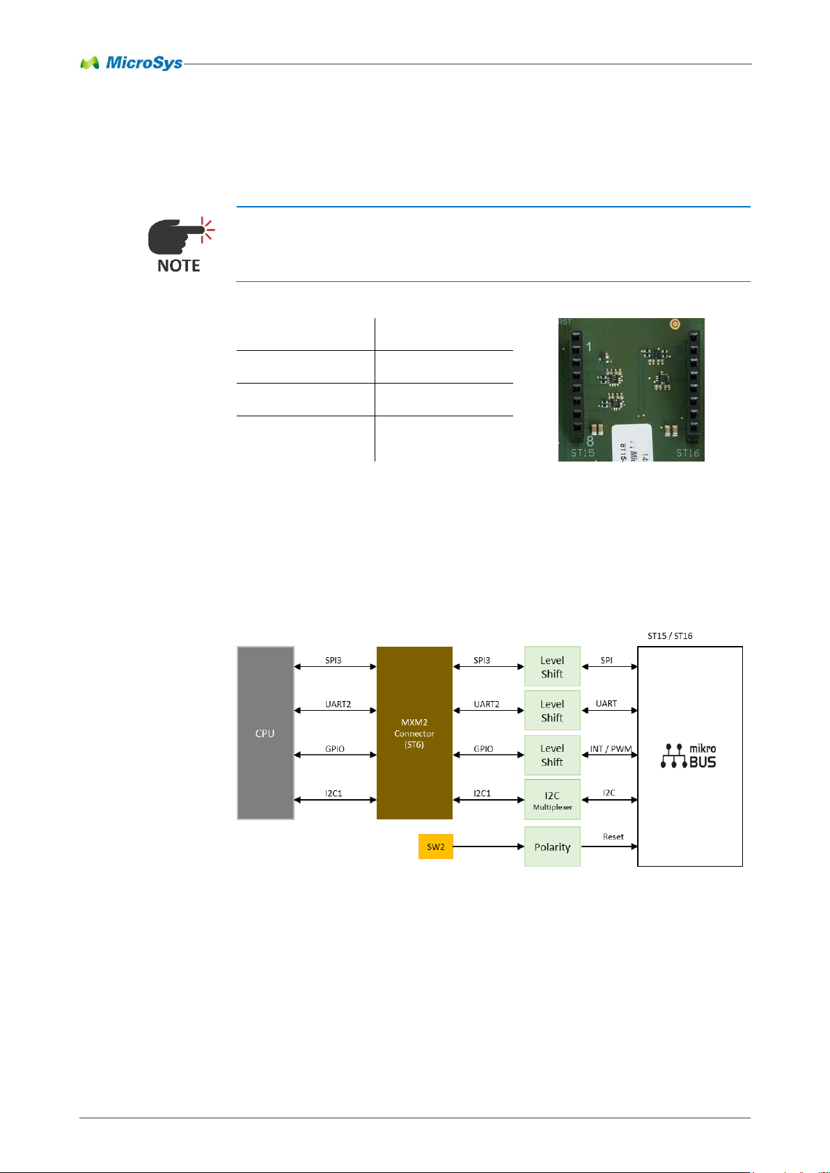
6.9 mikroBus™-Interface ................................... 49
6.10 JTAG Connector .......................................... 51
JTAG for module ......................................... 51
JTAG on carrier ........................................... 52
6.11 Fan Connector ............................................. 53
6.12 Test Connector ............................................ 53
7 Switches, Buttons and Jumpers .............. 54
7.1 Boot Device Switch ...................................... 54
7.2 Board Configuration Switch ......................... 55

Table of Contents
miriac SBC-LS1028A User Manual
V 1.0
3/65
© MicroSys Electronics GmbH 2019
7.3 Reset Button ............................................... 56
8 LEDs ........................................................... 57
8.1 Power And Reset LEDs ............................... 57
8.2 RJ45 LEDs .................................................. 58
8.3 LEDs on MPX-LS1028A .............................. 59
9 Software ..................................................... 60
9.1 U-Boot ......................................................... 60
9.2 Operating System Support .......................... 60
10 Known Issues ............................................ 61
11 Appendix .................................................... 62
11.1 Acronyms ..................................................... 62
11.2 Table of Figures ........................................... 63
11.3 Table of Tables ............................................ 64
12 History ........................................................ 65

General Notes 1
miriac SBC-LS1028A User Manual
V 1.0
4/65
© MicroSys Electronics GmbH 2019
1 General Notes
Copyright MicroSys Electronics GmbH, September 2019
All rights reserved. All rights in any information which appears in this document
belong to MicroSys Electronics GmbH or our licensors. You may copy the
information in this manual for your personal, non-commercial use.
Copyrighted products are not explicitly indicated in this manual. The absence of the
copyright (©) and trademark (TM or ®) symbols does not imply that a product is not
protected. Additionally, registered patents and trademarks are similarly not
expressly indicated in this manual.
1.1 Warranty
To the extent permissible by applicable law all information in this document is
provided without warranty of any kind, whether expressed or implied, including but
not limited to any implied warranty of satisfactory quality or fitness for a particular
purpose, or of non-infringement of any third party’s rights. We try to keep this
document accurate and up-to-date but we do not make any warranty or
representation about such matters. In particular we assume no liability or
responsibility for any errors or omissions in this document.
MicroSys Electronics GmbH neither gives any guarantee nor accepts any liability
whatsoever for consequential damages resulting from the use of this manual or its
associated product.
MicroSys Electronics GmbH further reserves the right to alter the layout and/or
design of the hardware without prior notification and accepts no liability for doing
so.
1.2 Links
We make no warranty about any other sites that are linked to or from this
document, whether we authorise such links or not.
1.3 Liability
To the extent permissible by applicable law, in no circumstance, including (but not
limited to) negligence, shall we be liable for your reliance on any information in this
document, nor shall we be liable for any direct, incidental, special, consequential,
indirect or punitive damages nor any loss of profit that result from the use of, or the
inability to use, this document or any material on any site linked to this document
even if we have been advised of the possibility of such damage. In no event shall
our liability to you for all damages, losses and causes of action whatsoever,
whether in contract, tort (including but not limited to negligence) or otherwise
exceed the amount, if any, paid by you to us for gaining access to this document.
MicroSys Electronics GmbH
Muehlweg 1
82054 Sauerlach
Germany
Phone: +49 8104 801-0
Fax: +49 8104 801-110

General Notes 1
miriac SBC-LS1028A User Manual
V 1.0
5/65
© MicroSys Electronics GmbH 2019
1.4 Offer to Provide Source Code of Certain
Software
This product contains copyrighted software that is licensed under the General
Public License (“GPL”) and under the Lesser General Public License Version
(“LGPL”). The GPL and LGPL licensed code in this product is distributed without
any warranty. Copies of these licenses are included in this product.
You may obtain the complete corresponding source code (as defined in the GPL)
for the GPL Software, and/or the complete corresponding source code of the LGPL
Software (with the complete machine-readable “work that uses the Library”) for a
period of three years after our last shipment of the product including the GPL
Software and/or LGPL Software, which will be no earlier than December 1, 2010,
for the cost of reproduction and shipment, which is dependent on the preferred
carrier and the location where you want to have it shipped to, by sending a request
to:
MicroSys Electronics GmbH
Muehlweg 1
82054 Sauerlach
Germany
In your request please provide the product name and version for which you wish to
obtain the corresponding source code and your contact details so that we can
coordinate the terms and cost of shipment with you.
The source code will be distributed WITHOUT ANY WARRANTY and licensed
under the same license as the corresponding binary/object code.
This offer is valid to anyone in receipt of this information.
MicroSys Electronics GmbH is eager to duly provide complete source code as
required under various Free Open Source Software licenses. If however you
encounter any problems in obtaining the full corresponding source code we would
be much obliged if you give us a notification to the email address
gpl@microsys.de, stating the product and describing the problem (please do NOT
send large attachments such as source code archives etc to this email address)
General Notes 1
miriac SBC-LS1028A User Manual
V 1.0
6/65
© MicroSys Electronics GmbH 2019
1.5 Symbols, Conventions and Abbreviations
Symbols
Throughout this document, the following symbols will be used:
Information marked with this symbol MUST be obeyed to avoid
the risk of severe injury, health danger, or major destruction of
the unit and its environment
Information marked with this symbol MUST be obeyed to avoid
the risk of possible injury, permanent damage or malfunction of
the unit.
Information marked with this symbol gives important hints upon
details of this manual, or in order to get the best use out of the
product and its features.
Table 1-1 Symbols
Conventions
Symbol
explanation
#
denotes a low active signal
←
denotes the signal flow in the shown direction
→
denotes the signal flow in the shown direction
↔
denotes the signal flow in both directions
→
denotes the signal flow in the shown direction with additional logic /
additional ICs in the signal path
I/O
denotes a bidirectional pin
Input
denotes an input pin
matched
denotes the according signal to be routed impedance controlled and
length matched
Output
denotes an output pin
Pin 1
refers to the numeric pin of a component package
Pin a1
refers to the array position of a pin within a component package
XXX-
denotes the negative signal of a differential pair
XXX+
denotes the positive signal of a differential pair
XXX
denotes an optional not mounted or fitted part
Table 1-2 Conventions
Introduction 2
miriac SBC-LS1028A User Manual
V 1.0
7/65
© MicroSys Electronics GmbH 2019
2 Introduction
Thank you for choosing the MicroSys SBC-LS1028A Single Board Computer
system. This manual will provide information for best performance and detailed
description of all available features.
2.1 Safety and Handling Precautions
ALWAYS use the correct type and polarity of the power supply!
DO NOT exceed the rated maximum values for the power supply! This may result in
severe permanent damage to the unit, as well as possible serious injury.
ALWAYS keep the unit dry, clean and free of foreign objects. Otherwise, irreparable
damage may occur.
Parts of the unit may become hot during operation. Take care not to touch any parts
of the circuitry during operation to avoid burns, and operate the unit in a wellventilated location. Provide an appropriate cooling solution as required
ALWAYS take ESD precautions when handling the unit.
Many pins on external connectors are directly connected to the CPU or other ESD
sensitive devices.
Make or break ANY connections ONLY while the unit is switched OFF.
Otherwise, permanent damage to the unit may occur, which is not covered by
warranty..
There is no separate SHIELD connection.
All the metal sheaths of shielded connectors are connected to GND.
Carrier board mounting holes are not connected to GND.
The module’s mounting holes are not connected to GND
Take this into account when handling and mounting the unit
Introduction 2
miriac SBC-LS1028A User Manual
V 1.0
8/65
© MicroSys Electronics GmbH 2019
2.2 Short Description
The SBC-LS1028A is a small computer system consisting of
■ the MPX-LS1028A module, based on NXP’s LS1028A Industrial Applications
Processor
■ and the CRX07 carrier board.
It targets both
■ evaluation of the respective MPX-LS1028A SOM
■ direct usage as an industrial computing solution
This document gives you an overview on the board's hardware features and capabilities and how to take the first steps on the initial setup.
2.3 Shipping List
The SBC-LS1028A Development Kit (Article No.857602) contains the following
items:
■ The SBC-LS1028A system, mounted with a heatsink
■ Power Supply 12V DC stabilized / 2 A
■ USB cable type A – mini B
■ microSD card with U-Boot, Linux and root file system installed
■ USB stick with documentation and source code
2.4 Feature Changelist for HW Revisions
Revision 1
Revision 1 is the first revision.
Revision 2
■ Changed ST4 to MIPI-10 connector
■ Added USB support to ST7 and ST8 mini PCIe slots
Introduction 2
miriac SBC-LS1028A User Manual
V 1.0
9/65
© MicroSys Electronics GmbH 2019
2.5 Functional Coverage
The following table shows the features available on the SBC-LS1028A:
Native CPU Interface
Availability
Used As
SerDes 0
✓
10/100/1000 MBit LAN
via SGMII
SerDes 1
✓
4x 10/100/1000 MBit LAN
via QSGMII
SerDes 2
✓
mPCIe
SerDes 3
✓
mPCIe/ mSATA
EC 1
✓
10/100/1000 MBit LAN
via RGMII
USB 1
✓
USB 2.0 / 3.0 (Host)
USB 2
✓
USB 2.0 / 3.0 (Host)
SDHC 1
✓
1bit / 4 bit SD-Card
(configurable as boot device)
SDHC 2
✓
1bit / 8 bit eMMC
UART 1
✓
UART to USB
(debug console)
UART 2
✓
mikroBUS
SPI 3 ✓ mikroBUS
XSPI 1
✓
QSPI boot flash
(2 selectable boot devices)
I²C 1
✓
I²C with multiple devices
I²C 2
---
Card Detect / Write Protect
(SD-Card)
I²C 3
---
CAN-FD 1
I²C 4
---
CAN-FD 2
I²C 5
---
mikroBUS
(INT and PWM)
I²C 6
---
USB2 power fault & power enable
I²C 7
---
SDHC2
(Data 4 , 5)
I²C 8
---
SDHC2
(Data 6 , 7)
CAN ✓ 2x CAN FD
DisplayPort
✓
DisplayPort
JTAG
✓
Signals on standard MIPI-10
connector
RTC
✓
RTC with backup (supercap)
Reset
✓
Button, LED
Table 2-1 Functional coverage
Quick Start Guide 3
miriac SBC-LS1028A User Manual
V 1.0
10/65
© MicroSys Electronics GmbH 2019
3 Quick Start Guide
3.1 Prerequisites
Always make sure to handle the SBC-LS1028A unit in an ESD-safe manner.
Otherwise, the unit may suffer permanent damage.
Do not place the unit directly flat on a metal surface, as this may result in short
circuits and damage to the board.
First unpack the unit and make sure that it is clean and free of visible damage or
foreign objects.
Minimum Requirements
To operate the board, you will at least need the following items:
■ a 12V DC (min 2A) power supply – delivered with the kit
■ a USB cable (type A – mini B) – delivered with the kit
■ a serial terminal, such as a PC with a USB port running a terminal Software
(e.g. TeraTerm, HyperTerminal, putty, ckermit...), or else a hardware serial
console. Choose the following parameters:
(a) 115200 Bd
(b) 8 Data bits
(c) No parity
(d) 1 Stop Bit
Recommended Items
The following items are not absolutely necessary, but strongly recommended for
practical operation and development purposes:
■ SATA HDD/SSD and/or SD card as mass storage and/or boot media
■ Network connection to your local network
■ TFTP server available for downloading within the network
The TFTP server may run on the same PC as the serial terminal
Quick Start Guide 3
miriac SBC-LS1028A User Manual
V 1.0
11/65
© MicroSys Electronics GmbH 2019
3.2 Board Preparation and Power-Up
■ Make sure the switches SW1 and SW2 are set properly in order to select the
correct boot source and board configuration (refer to chapter 7.1).
■ The board comes preconfigured to boot correctly on arrival.
■ Connect the mini USB cable to ST14.
■ Connect other peripherals (USB, LAN, mSATA, ...) as needed.
■ Connect the power supply to the ST20 connector, while the power supply is
still switched off.
■ Switch on the power.
Figure 3-1 System setup example
Power supply
USB cable (serial console)
Ethernet cable
Quick Start Guide 3
miriac SBC-LS1028A User Manual
V 1.0
12/65
© MicroSys Electronics GmbH 2019
3.3 Operation
After power-on, the green LED on the module should light up and any red LED should
be off.
IF NOT, DISCONNECT THE UNIT FROM POWER AND CHECK FOR FAULTS!
U-Boot Startup
When power is supplied the system will start and boot messages from U-Boot will
appear on the serial console.
The exact output may vary, depending on U-Boot and MPX-LS1028A module versions
in use.
U-Boot SPL 2018.09-1.3.0 (Sep 06 2019 - 10:44:39 +0200)
Initializing DDR....
Trying to boot from MMC1
U-Boot 2018.09-1.3.0 (Sep 06 2019 - 10:44:39 +0200)
SoC: LS1028AE Rev1.0 (0x870b0010)
Clock Configuration:
CPU0(A72):1300 MHz CPU1(A72):1300 MHz
Bus: 400 MHz DDR: 1600 MT/s
Reset Configuration Word (RCW):
00000000: 34004010 00000030 00000000 00000000
00000010: 00000000 008f0000 0030c000 00000000
00000020: 01e021a0 00002580 00000000 0000b296
00000030: 00000000 00000048 00000000 00000000
00000040: 00000000 00000000 00000000 00000000
00000050: 00000000 00000000 00000000 00000000
00000060: 00000000 00000000 00167000 00000000
00000070: eb580000 03000000
Model: MicroSys MPXLS1028
I2C: ready
DRAM: Detected UDIMM Fixed DDR on board
3.9 GiB (DDR4, 32-bit, CL=11, ECC on)
FSL_SDHC: 0, FSL_SDHC: 1
Releasing PCI reset ...
Using SERDES1 Protocol: 60248 (0xeb58)
PCIe0: pcie@3400000 disabled
PCIe1: pcie@3500000 Root Complex: no link
Waking secondary cores to start from fbd64000
All (2) cores are up.
Quick Start Guide 3
miriac SBC-LS1028A User Manual
V 1.0
13/65
© MicroSys Electronics GmbH 2019
WARNING: Calling __hwconfig without a buffer and before environment is ready
MMC: Loading Environment from MMC... OK
In: serial
Out: serial
Err: serial
SATA link 0 timeout.
AHCI 0001.0301 32 slots 1 ports 6 Gbps 0x1 impl SATA mode
flags: 64bit ncq pm clo only pmp fbss pio slum part ccc apst
Found 0 device(s).
SCSI:
Net:
setting up RGMII
=>
Linux
For detailed setup instructions, refer to the PDF document
“Linux_4.x_Yocto_SDK_User_Manual” provided on the USB stick which is delivered with the Development Kit.
System Description 4
miriac SBC-LS1028A User Manual
V 1.0
14/65
© MicroSys Electronics GmbH 2019
4 System Description
This section describes all parts of the SBC-LS1028A system.
4.1 Block Diagram
4.2 Feature Overview
The SBC-LS1028A offers the following features:
Features
Processor
NXP LS1028A with dual
Cortex-A72 cores
up to 1500MHz, no SEC
SDRAM
32-bit DDR4 interface
up to 4GBytes
up to 1600MT/s
4 x DDR4 (x8) + ECC
single bank
Boot Memory
QSPI NOR Flash
128 Mbits
Alternate Boot Memory
QSPI NAND Flash
4 Gbits
eMMC
SDHC2
8 GBytes (on carrier)
8-bit interface
4x SerDes
SGMII
10/100/1000 Mbps
TSN capability
PCIe Gen 3 @ 8Gbps
Lane x1, Root Complex
functionality
1x PCIe extension
connector
PCIe Gen 3 @ 8Gbps
Lane x1, Root Complex
functionality
1x mSATA / Mini PCIe
Slot
Figure 4-1 Block Diagram (MPX-LS1028A Rev. 2 on carrier CRX07 Rev. 2)
System Description 4
miriac SBC-LS1028A User Manual
V 1.0
15/65
© MicroSys Electronics GmbH 2019
Features
QSGMII
4x 10/100/1000 Mbps
TSN capability
Gigabit Ethernet
Controller
RGMII
10/100/1000 Mbps
USB
USB 3.0 Phy
USB connector type A
(USB1)
USB 3.0 Phy
USB connector type A
(USB2)
Expansion Cards
MMC/SD/SDIO
microSD card holder
Serial Interfaces
UART1
Converted to USB
(FT232),
available on USB
connector type mini B
UART2
Available on
MikroBus interface
I2C
I2C-1
400 kbps
Connected Devices:
- Temperature
Sensor
- EEPROM
- RTC
- GPIO Expander
- I2C Multiplexer
CAN
CAN1
CAN FD
CAN2
CAN FD
MikroBUS
2x GPIO
MikroBUS
INT and PWM
System JTAG
Controller
JTAG
10-pin MIPI header on
carrier
Power Management
Primary Supply
Input:
9-30V DC
Output:
5V DC / peak 8A
Backup Supply
(RTC backup)
Supercap
Table 4-1 Feature Overview
System Description 4
miriac SBC-LS1028A User Manual
V 1.0
16/65
© MicroSys Electronics GmbH 2019
4.3 Mechanical Dimensions
MPX-LS1028A
The following drawing shows the mechanical outline of the MPX-LS1028A module
that is plugged in the CRX07 carrier.
For 3D data files please contact MicroSys.
Figure 4-2 Mechanical Dimensions: Module
System Description 4
miriac SBC-LS1028A User Manual
V 1.0
17/65
© MicroSys Electronics GmbH 2019
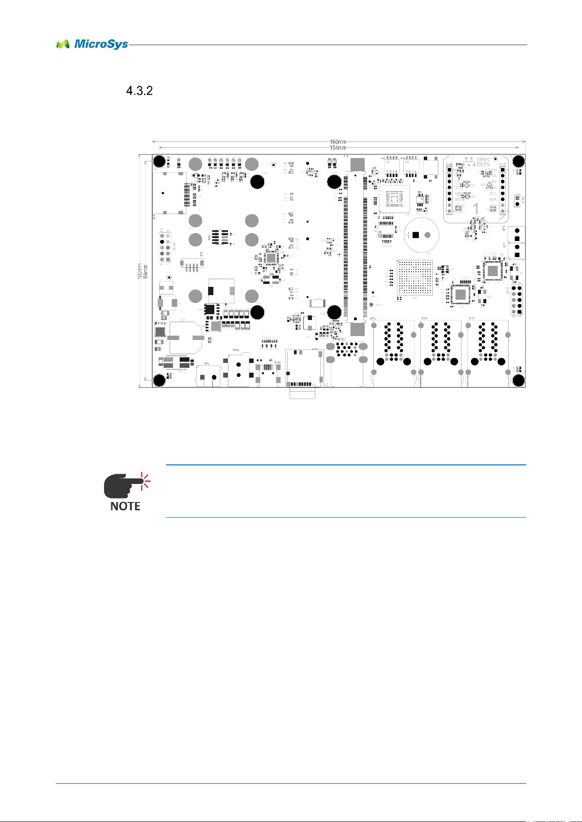
SBC-LS1028A
The following drawing shows the mechanical outline of the SBC-LS1028A.
For 3D data files please contact MicroSys.
Figure 4-3 Mechanical Dimensions: SBC-LS1028A Carrier
System Description 4
miriac SBC-LS1028A User Manual
V 1.0
18/65
© MicroSys Electronics GmbH 2019
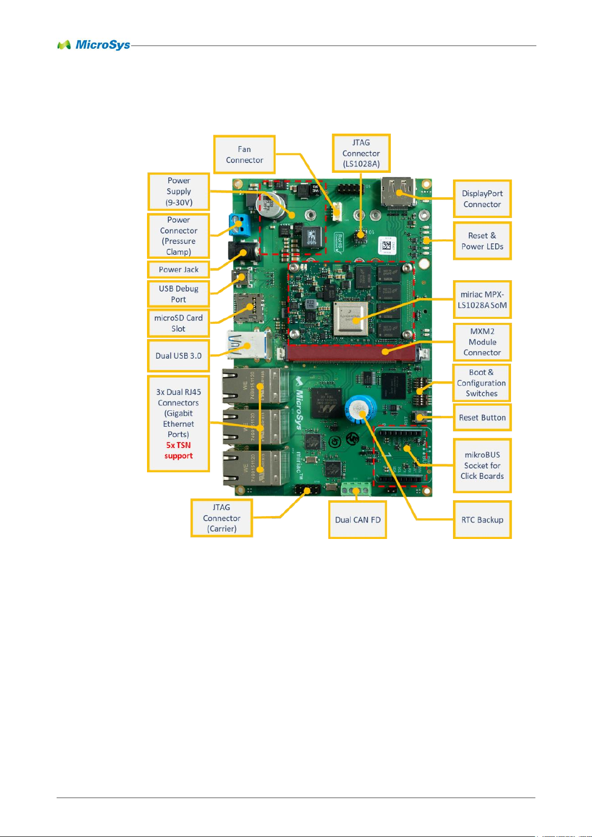
4.4 Connector Layout – Top
Figure 4-4 Top connectors
System Description 4
miriac SBC-LS1028A User Manual
V 1.0
19/65
© MicroSys Electronics GmbH 2019
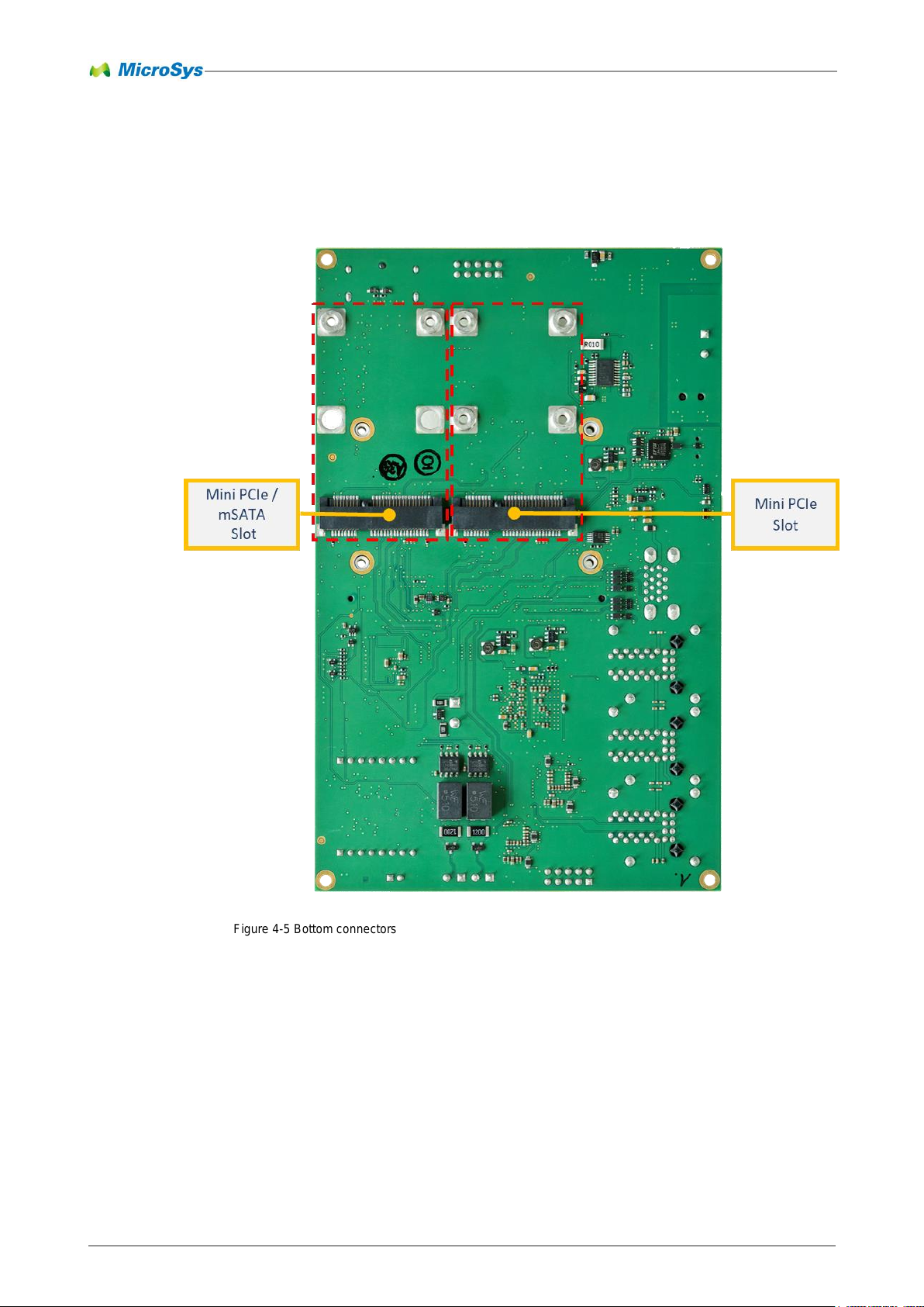
4.5 Connector Layout – Bottom
Figure 4-5 Bottom connectors

System Description 4
miriac SBC-LS1028A User Manual
V 1.0
20/65
© MicroSys Electronics GmbH 2019
4.6 Power Supply
Input Supply Rating
The SBC-LS1028A system is run from a single DC power supply with the following
ratings:
Maximum Input Voltage Operating Range:
9V - 30V DC
Nominal Input Supply Voltage:
12V DC
Typical Current Consumption
(@12V / room temperature / U-Boot prompt):
~0,53A
ALWAYS use the correct type and polarity of the power supply!
DO NOT exceed the rated maximum values for the power supply! This may result in
severe permanent damage to the unit, as well as possible serious injury.
Input Protection
The board is protected against wrong polarity and over-voltage spikes.
Transistor TR3 is installed for polarity protection. It is switched on only if power is
connected with correct polarity (+Vin connected to Pin 1). Otherwise, TR3 will stay
off and no internal voltages are generated.
Over-voltage is limited to 33V by a TVS diode. Spikes higher than 33V will be cut
off. Please note that applying a permanent power higher than the breakdown
voltage will destroy the TVS diode.

System Description 4
miriac SBC-LS1028A User Manual
V 1.0
21/65
© MicroSys Electronics GmbH 2019
Input Power Connector 1 (Pressure Clamp)
Part Reference
ST9
Manufacturer:
Würth Elektronik
Type:
691101710002
Pinout:
Pin
Silkscreen Label
Signal
Function
1
„VIN“
+VIN
Power
2
„GND“
GND
Ground
Table 4-1 Pinout Pressure Clamp
Input Power Connector 2 (Power Jack)
Part Reference
ST20
Manufacturer:
Würth Elektronik
Type:
694106106102
Pinout:
Pin
Signal
Function
1
+VIN
Power
2
GND
Ground
Table 4-2 Pinout Power Jack

System Description 4
miriac SBC-LS1028A User Manual
V 1.0
22/65
© MicroSys Electronics GmbH 2019
Power Supply Structure
■ Input power from ST9 / ST20 connector is fed to the primary step-down
converter.
■ The primary step-down converter produces 5V DC / max. 8A peak from the
input supply which supplies both the MPX-LS1028A module and peripheral
devices on the carrierboard CRX07.
■ The 5V DC are fed to a secondary step-down converter, which produces 3.3V
DC / max. 4A peak.
■ Three NCP1529 produce 1.8V and 1.0V from +5V and 1.5V from 3.3V, which
are used for both PCIe and onboard devices.
The following diagram shows the power supply structure:
RTC Backup Battery
The RTC on the module is supplied from a 470mF supercap that is charged by the
5V power source on the carrier.
Figure 4-6 Power supply structure

System Description 4
miriac SBC-LS1028A User Manual
V 1.0
23/65
© MicroSys Electronics GmbH 2019
Current Measurement
For current measurements the carrier provides a 10mΩ shunt resistor in the 5V
path supplying the CPU module.
The carrier also provides an I²C current sense amplifier for automated
measurements. See chapter 5.7 for more details.
Voltage Monitoring
The carrier monitors onboard-generated voltages and resets the module in case
any voltage drops below the undervoltage limit:
Voltage
Monitoring
Threshold (typ.)
Threshold (min./max.)
5,0V
Undervoltage
4,625V
4,556V / 4,694V
3,3V
Undervoltage
3,108V
3,038V / 3,180V
1,8V
Undervoltage
1,680V
1,642V / 1,719V
1,5V
Undervoltage
1,390V
1,361V / 1,420V
1,0V
Undervoltage
0,899V
0,885V / 0,915V
Table 4-3 Voltage monitoring limits (carrier)
Fuses
There are no fuses on the SBC-LS1028A.

System Core, Boot Configuration and On-Board Memory 5
miriac SBC-LS1028A User Manual
V 1.0
24/65
© MicroSys Electronics GmbH 2019
5 System Core, Boot Configuration
and On-Board Memory
5.1 Processor NXP LS1028A
The QorIQ Layerscape LS1028A processor from NXP contains dual Arm CortexA72 cores. It exposes a wide variety of external interfaces, which are explained in
detail in the following chapters.
The two cores run at a maximum clock speed of 1500 MHz. The CPU frequency
can be clocked down if necessary. Both cores share a single 1MB L2 cache.
5.2 JTAG Chain
The SBC-LS1028A has two separate JTAG chains divided into devices on the
carrier board and devices on the CPU module.
Carrier
The JTAG chain on the carrier (connector ST19) connects to the QSGMII PHY
only.
The pinout allows direct connection of the Goepel TAP header, for example.
CPU Module
The JTAG chain on the module includes the LS1028A processor only. Its JTAG
port is accessible on the carrier at connector ST4.
The JTAG connector footprint provides JTAG signals on a MIPI-10 connector.
Both JTAG and Boundary Scan connections can be established.
SW2 switches between these two modes (see chapter 7.2).
Please see chapter 6.10 for a description of the JTAG connector.

System Core, Boot Configuration and On-Board Memory 5
miriac SBC-LS1028A User Manual
V 1.0
25/65
© MicroSys Electronics GmbH 2019
5.3 Reset Structure
Pin
Number
on ST6
Signal Name
Signal
Direction
Function
T7
RSTIN#
Input to the
module
Active low module reset:
while active the module is held in reset state
T5
HRST#
Output from
the module
Active low peripheral reset:
while active peripheral devices shall be held in
reset state
B4
WDOG-TRIG#
Output from
the module
Watchdog service signal from the module which
has to be triggered periodically. When the
watchdog is active and the service stops the
module will be reset.
The watchdog is enabled with the first falling edge
of the WDOG-TRIG# signal.
Once enabled, the watchdog will only be disabled
when a board reset or power cycle occurs.
B77
BSCAN-EN#
Input to the
module
Active low boundary scan enable signal.
B78
JTRST#
Input to the
module
Active low JTAG reset signal:
Depending on “BSCAN-EN” this reset will be
treated differently on the CPU module
B3
PCIE-RST#
Output from
the module
Active low PERST# reset:
Auxiliary reset signal to reset connected PCIe
devices
Table 5-1 Reset signal overview
Figure 5-1 Reset Structure (carrier CRX07)

System Core, Boot Configuration and On-Board Memory 5
miriac SBC-LS1028A User Manual
V 1.0
26/65
© MicroSys Electronics GmbH 2019
RSTIN# / HRST#
The RSTIN# is an input to the module. When inactive it signals that the voltage
supplies on the carrier are within their limits and no manual reset was triggered.
When active (signal is low) the monitoring unit on the module initiates the reset sequence in order to keep the CPU in a defined reset state. No further interaction
from the carrier is necessary. In case the module reset is active, the CPU triggers
the HRST# signal which is intended to control the reset of peripheral devices on
the carrier i.e. Ethernet PHYs, PCIe slots and other devices.
The RSTIN# signal can be triggered by either a power-fault situation, a manual
reset button (“SW3”) or a missing watchdog trigger signal “WD-TRIG#” from the
CPU - provided that the watchdog was previously enabled.
Watchdog
The carrier board provides a watchdog (J5 / MIC826) which can be enabled by
pulling the signal “WD-TRIG” (ST6, pin B4) low once after the carrier board reset
has been released. If enabled the watchdog will only be disabled when a board
reset or power cycle occurs. It must be serviced periodically by the “WD-TRIG”
signal within the timeout period of 1.6s (typical).
In case no event is triggered the “RSTIN#” goes low and the module is held in
reset.
JTAG / Boundary Scan
Starting with revision 2 of the carrier there is a MIPI-10 connector available. In
conjunction with SW2 the user can choose between the ARM-10-JTAG pinout and
the MIPI-10-nTRST pinout. More information can be found on the Lauterbach
homepage.
Basically the MIPI-10-nTRST pinout is intended for Boundary Scan and can be
enabled via SW2. The difference is how the resets on the module connect to the
CPU.
PCI Express Reset
PCIE-RST# is an auxiliary reset signal for PCIe devices to implement the
Fundamental Reset (“PERST#”).

System Core, Boot Configuration and On-Board Memory 5
miriac SBC-LS1028A User Manual
V 1.0
27/65
© MicroSys Electronics GmbH 2019
5.4 Clock Distribution
The following diagram shows the clock distribution of the SBC-LS1028A system:
Figure 5-2 Clock distribution

System Core, Boot Configuration and On-Board Memory 5
miriac SBC-LS1028A User Manual
V 1.0
28/65
© MicroSys Electronics GmbH 2019
5.5 Boot Options
The SBC-LS1028A board offers a selection of four possible boot devices. Two are
QSPI devices and the other two are SDHC devices.
Selection is made via SW1 (see chapter 7.1). SW1 configures four boot select pins
which are directly connected to the CPU. They are sampled on the rising edge of
the reset. Those pins carry alternate functions, too, thus they can be used elsewhere. Additionally, the “BOOT_INV” signal (ST6, pin T4) switches the chip selects
of the QSPI devices depending on the boot mode.
The boot pins have a default high state (pullups are on the carrier) when SW1 is
off. When the switch is on, the respective pin is grounded.
The boot pins are decoded as follows (1= high, 0=low):
Boot Source
Chip Select
Boot
INV
Signals [ST6]
DIP Switch
CS0#
[BOOT]
CS1#
T4
B 8 B 9 B
90 B 87
4 3 2
1
SDHC1:
SD-Card
NOR
NAND
0 1 0 0 0
OFF
ON
ON
ON
SDHC2:
eMMC
NOR
NAND
0 1 0 0 1
OFF
ON
ON
OFF
QSPI NAND
Flash
(4KB pages)
NAND
NOR
1 1 1 0 1
OFF
OFF
ON
OFF
QSPI NOR
Flash
NOR
NAND
0 1 1 1 1
OFF
OFF
OFF
OFF
Table 5-2 Hard-wired boot signals

System Core, Boot Configuration and On-Board Memory 5
miriac SBC-LS1028A User Manual
V 1.0
29/65
© MicroSys Electronics GmbH 2019
5.6 QSPI Flash
There are two different flashes on the CPU module which can be accessed by
means of chip select CS0# and CS1#.
Device access (CSx#) depends on the “BOOT_INV” signal (see chapter 5.5)
QSPI NAND Flash
The SBC-LS1028A system is equipped with 512MB of Serial NAND Flash by
default. Different sizes may be available on request/order. The following table
shows the connections and signal levels of the Serial NAND Flash.
LS1028A
I/O
Range
QSPI Serial NAND Flash
TC58CYG2S0HRAIG
Pin
Name
Pin
Name
H12 /
D12
XSPI1_A_CS0# /
XSPI1_A_CS1#
→
LVTTL 1 CS
H10
XSPI1_A_SCK
→
LVTTL 6 CLK
4 / 9
GND
G11
XSPI1_A_DATA0
↔
LVTTL 5 SO0
F12
XSPI1_A_DATA1
↔
LVTTL 2 SO1
H14
XSPI1_A_DATA2
↔
LVTTL 3 SO2
E13
XSPI1_A_DATA3
↔
LVTTL 7 SO3 8 +1.8V
Table 5-3 QSPI Serial NAND Flash pin assignments

System Core, Boot Configuration and On-Board Memory 5
miriac SBC-LS1028A User Manual
V 1.0
30/65
© MicroSys Electronics GmbH 2019
QSPI NOR Flash
The SBC-LS1028A system is equipped with 16MB of QSPI NOR Flash by default
on the LS1028A’s QSPI port. Up to 128 MB are available on request/order.
LS1028A
I/O
Range
QSPI NOR Flash
MT25QU128ABA8E12
Pin
Name
Pin
Name
H12 /
D12
XSPI1_A_CS0#
XSPI1_A_CS1#
→
LVTTL
C2
CS
H10
XSPI1_A_SCK
→
LVTTL
B2
CLK
B3
GND
G11
XSPI1_A_DATA0
↔
LVTTL
D3
DQ0
F12
XSPI1_A_DATA1
↔
LVTTL
D2
DQ1
H14
XSPI1_A_DATA2
↔
LVTTL
C4
DQ2
E13
XSPI1_A_DATA3
↔
LVTTL
D4
DQ3
B4
+1.8V
Table 5-4 QSPI NOR Flash pin assignment

System Core, Boot Configuration and On-Board Memory 5
miriac SBC-LS1028A User Manual
V 1.0
31/65
© MicroSys Electronics GmbH 2019
5.7 I²C Bus
The SBC-LS1028A offers one I²C bus: I2C-1. As the bus is already used on the
module some I²C addresses are not available. The carrier adds an I²C multiplexer:
The following table shows the I²C addresses depicted as 7-bit addresses. The R/W
bit is not displayed.
I2C-1 bus map (7-bit address):
Address
Designator
Device
On
Carrier
On
Module
Function
0x43
J12
FXL6408
✓ GPIO Expander
0x00
J30
TMP451AIDQF
✓
General Call reset
address
0x4C
Temperature sensor
0x51
J7
PCF85063ATT
✓ RTC
0x54
J10
BR24G128NUX-3
✓ EEPROM
0x70
J24
TCA9544APWR
✓
I²C Multiplexer
Table 5-5 I²C-1 bus map
Figure 5-3 Multiplexer I2C-1 bus
Figure 5-4 I2C-1 bus topology

Peripherals 6
miriac SBC-LS1028A User Manual
V 1.0
32/65
© MicroSys Electronics GmbH 2019
6 Peripherals
6.1 Connector References
Reference
Function
Populated?
Top / Bottom
ST1
CAN1 clamping socket
✓
Top
ST2
CAN2 clamping socket
✓
Top
ST3
Fan connector
✓
Top
ST4
JTAG connector (module)
✓
Top
ST5
DisplayPort Connector
✓
Top
ST6
MXM2 module connector
✓
Top
ST7
mPCIe slot
✓
Bottom
ST8
mPCIe / mSATA slot
✓
Bottom
ST9
Power connector, pressure
clamp
✓
Top
ST10
Dual RJ45 connector
✓
Top
ST11
Dual RJ45 connector
✓
Top
ST12
Dual RJ45 connector
✓
Top
ST13
microSD slot
✓
Top
ST14
Mini USB connector
✓
Top
ST15
mikroBUS connector 1
✓
Top
ST16
mikroBUS connector 2
✓
Top
ST17
Dual USB connector Type A
✓
Top
ST18
Fuse programming connector
✓
Top
ST19
JTAG connector (carrier)
✓
Top
ST20
Power plug
✓
Top
ST21
Test connector
✓
Top
Table 6-1 Connector reference overview

Peripherals 6
miriac SBC-LS1028A User Manual
V 1.0
33/65
© MicroSys Electronics GmbH 2019
6.2 Module Connector
The CRX07 carrier provides an MXM2 connector which accepts compatible
MicroSys CPU modules.
Part Reference:
ST6
Manufacturer:
Iriso
Pin Count:
230
Type:
IMSA-18010S-230A-GN1
Used with:
MicroSys CPU modules
6.3 LAN Connections
The SBC-LS1028A system offers six independent Gigabit LAN connections. These
six ports are distributed over three connectors named ST10, ST11 and ST12. The
connectors have integrated magnetics.
The following picture shows the front view of the three connectors as placed on the
CRX07 baseboard. For further information on the LEDs please see chapter 8.
Part Reference:
ST10, 11, 12
Manufacturer:
Würth Elektronik
Type:
749 915 1120
Mates with:
RJ45 patch ca-
ble, category
depends on
speed
Port
Serdes Lane
on ST6
RGMII
on ST6
PHY address
SGMII
Lane 0
---
0000
RGMII
---
RGMII
0001
QSGMII 0
Lane 1
---
0100
QSGMII 1
---
0101
QSGMII 2
---
0110
QSGMII 3
---
0111
Table 6-2 LAN / DTSEC / SerDes / RGMII assignment

Peripherals 6
miriac SBC-LS1028A User Manual
V 1.0
34/65
© MicroSys Electronics GmbH 2019
The LAN Sockets have a standard layout for Gigabit Ethernet, i.e. the pairs are 1-2,
3-6, 4-5 and 7-8.
Pin
Pair 1 D-A+ 2 D-A- 3 D-B+
4
D-C+ 5 D-C- 6 D-B- 7 D-D+ 8 D-D-
Table 6-3 LAN Gigabit Ethernet connector pairs
SGMII
SGMII is connected to a standard RJ45 socket ST12. It uses the SerDes Lane 0
provided by the LS1028A configured as an SGMII port. The SGMII lane connects
to a Marvell PHY 88E1512P PHY.
LS1028A
ST6
88E1512P
Pin
Name
Pin
Signal
Pin
Name
AF12
SD1-TX0_P
→
T55
SD1-TX0_P
→ 1 S_INP
AG13
SD1-TX0_N
→
T54
SD1-TX0_N
→ 2 S_INN
AK10
SD1-RX0_P
←
T58
SD1-RX0_P
← 4 S_OUTP
AJ11
SD1-RX0_N
←
T57
SD1-RX0_N
← 5 S_OUTN
Table 6-4 SerDes 0 pin assignment
Figure 6-1 SGMII topology

Peripherals 6
miriac SBC-LS1028A User Manual
V 1.0
35/65
© MicroSys Electronics GmbH 2019
RGMII
The RGMII port is connected to a standard RJ45 socket ST12. It uses the Ethernet
controller EC1 of the LS1028A as an RGMII port. The RGMII lane connects to a
Marvell PHY 88E1512P PHY.
The following table shows the internal connections for the RGMII port:
LS1028A
ST6
88E1512P
I/O
Pin
Name
Pin
Signal
Pin
Name
Range
Pull-up
Pull-
down
AD2
EC1_RX_CLK
←
B53
EC1_RX_CLK
←
46
RX_CLK
1.8V
AH2
EC1_RX_DV
←
B52
EC1_RX_DV
←
43
RX_CTRL
1.8V
AF2
EC1_RXD0
←
B58
EC1_RXD0
←
44
RXD0
1.8V
AA1
EC1_RXD1
←
B57
EC1_RXD1
←
45
RXD1
1.8V
AE3
EC1_RXD2
←
B56
EC1_RXD2
←
47
RXD2
1.8V
AE1
EC1_RXD3
←
B55
EC1_RXD3
←
48
RXD3
1.8V
AH4
EC1_GTX_CLK
→
T71
EC1_GTX_CLK
→
53
TX_CLK
1.8V
AF6
EC1_TXD0
→
T69
EC1_TXD0
→
50
TXD0
1.8V
AF4
EC1_TXD1
→
T68
EC1_TXD1
→
51
TXD1
1.8V
AD4
EC1_TXD2
→
T67
EC1_TXD2
→
54
TXD2
1.8V
AG5
EC1_TXD3
→
T66
EC1_TXD3
→
55
TXD3
1.8V
AJ3
EC1_TX_EN
→
T64
EC1_TX_EN
→
56
TX_CTRL
1.8V 4k7
AK4
EMII_MDIO
↔
T60
EMII_MDIO
↔ 8 MDIO
1.8V
1k5 ||
10k
AK6
EMII_MDC
→
T62
EMII_MDC
→ 7 MDC
1.8V 4k7
AK2
EC1_GTX_CLK125
←
B60
EC1_GTX_CLK125
← 9 CLK125
1.8V
Table 6-5 Port RGMII pin assignment
Figure 6-2 RGMII topology

Peripherals 6
miriac SBC-LS1028A User Manual
V 1.0
36/65
© MicroSys Electronics GmbH 2019
QSGMII
SerDes Lane 1 provided by the LS1028A is configured as a QSGMII port that
connects to a Marvell PHY 88E1548P PHY. The four resulting MDI interfaces are
available through standard RJ45 sockets named ST10 and ST11.
LS1028A
ST6
88E1548P
Pin
Name
Pin
Signal
Pin
Name
AF14
SD1-TX1_P
→
T49
SD1-TX1_P
→
B9
Q_INP
AG15
SD1-TX1_N
→
T48
SD1-TX1_N
→
A9
Q_INN
AK12
SD1-RX1_P
←
T52
SD1-RX1_P
←
A8
Q_OUTP
AJ13
SD1-RX1_N
←
T51
SD1-RX1_N
←
B8
Q_OUTN
Table 6-6 SerDes 1 pin assignment
Figure 6-3 QSGMII topology

Peripherals 6
miriac SBC-LS1028A User Manual
V 1.0
37/65
© MicroSys Electronics GmbH 2019
6.4 PCIe Connections
The SBC-LS1028A offers two single lane PCIe interfaces on ST7 and ST8.
Table 6-7 PCIe SerDes assignment
Mini PCIe Slot
There are two mini PCIe slots, each with USB support, on the carrier.
ST7 can hold mPCIe cards only, mSATA is not supported.
Part Reference:
ST7
Manufacturer:
Tyco
Type:
2041119-1
Used with:
Half-size mini PCIe
cards are preferred
Broaching nuts for both half and full
size cards are placed on the carrier.
When full-size cards are used care
has to be taken to choose cards
that do not have parts on the
bottom side accidentally shorting
signals.
MicroSys recommends to use only
half-size cards with this slot!
Serdes
ST7
(Mini PCIe Slot)
ST8
(Mini PCIe / mSATA Slot)
Lane 2 ✓
Lane 3
✓

Peripherals 6
miriac SBC-LS1028A User Manual
V 1.0
38/65
© MicroSys Electronics GmbH 2019
Pin:
Pin:
1
WAKE#
+3.3Vaux
2 3 COEX1
GND
4 5 COEX2
+1.5V
6 7 CLKREQ#
UIM-PWR
8 9 GND
UIM-DAT
10
11
REFCLK-
UIM-CLK
12
13
REFCLK+
UIM-RST
14
15
GND
UIM-VPP
16
MECHANICAL KEY
17
Reserved
GND
18
19
Reserved
WDIS#
20
21
GND
PERST#
22
23
PER0-
+3.3Vaux
24
25
PER0+
GND
26
27
GND
+1.5V
28
29
GND
SMB-CLK
30
31
PET0-
SMB-DAT
32
33
PET0+
GND
34
35
GND
USB-D-
36
37
GND
USB-D+
38
39
+3.3Vaux
GND
40
41
+3.3Vaux
LED-WWAN#
42
43
GND
LED_WLAN#
44
45
Reserved
LED_WPAN#
46
47
Reserved
+1.5V
48
49
Reserved
GND
50
51
Reserved
+3.3Vaux
52
Table 6-8 mPCIe Slot pinout
The following table shows the internal connections:
LS1028A
ST6 ST7
Pin
Name
Pin
Signal
Pin
Name
AF16
SD1-TX2_P
→
T43
SD1-TX2_P
→
33
PET0_P
AG17
SD1-TX2_N
→
T42
SD1-TX2_N
→
31
PET0_N
AK14
SD1-RX2_P
←
T46
SD1-RX2_P
←
25
PER0_P
AJ15
SD1-RX2_N
←
T45
SD1-RX2_N
←
23
PER0_N
Table 6-9 mPCIe Slot SerDes 2 assignment
AC coupling capacitors for PER0_N and PER0_P have to be placed on
the plug-in card near the transmitter.

Peripherals 6
miriac SBC-LS1028A User Manual
V 1.0
39/65
© MicroSys Electronics GmbH 2019
Mini PCIe Slot / mSATA Slot
The second slot (ST8) can hold both mSATA cards and mPCIe cards. USB is also
supported.
Depending on the software configuration (SerDes configuration) either mSATA or
mPCIe cards can be used.
Part Reference:
ST8
Manufacturer:
Tyco
Type:
2041119-1
Used with:
Full-size or half-
size mini PCIe or
mSATA cards
Four holes for broaching nuts are
designed to allow for half and full
size cards to be used with this slot.
The broaching nuts for half-size
cards are not populated to allow
cards without height restrictions.

Peripherals 6
miriac SBC-LS1028A User Manual
V 1.0
40/65
© MicroSys Electronics GmbH 2019
Pin:
Pin:
1
WAKE#
+3.3Vaux
2 3 COEX1
GND
4 5 COEX2
+1.5V
6
7
CLKREQ#
UIM-PWR
8 9 GND
UIM-DAT
10
11
REFCLK-
UIM-CLK
12
13
REFCLK+
UIM-RST
14
15
GND
UIM-VPP
16
MECHANICAL KEY
17
Reserved
GND
18
19
Reserved
WDIS#
20
21
GND
PERST#
22
23
PER0+
+3.3Vaux
24
25
PER0-
GND
26
27
GND
+1.5V
28
29
GND
SMB-CLK
30
31
PET0-
SMB-DAT
32
33
PET0+
GND
34
35
GND
USB-D-
36
37
GND
USB-D+
38
39
+3.3Vaux
GND
40
41
+3.3Vaux
LED-WWAN#
42
43
GND
LED_WLAN#
44
45
Reserved
LED_WPAN#
46
47
Reserved
+1.5V
48
49
Reserved
GND
50
51
Reserved
+3.3Vaux
52
Table 6-10 mPCIe / mSATA Slot pinout
The following table shows the internal connections:
LS1028A
ST6 ST8
Pin
Name
Pin
Signal
Pin
Name
AF18
SD1-TX3_P
→
T37
SD1-TX3_P
→
33
PET0_P
AG19
SD1-TX3_N
→
T36
SD1-TX3_N
→
31
PET0_N
AK16
SD1-RX3_P
←
T40
SD1-RX3_P
←
23
PER0_N
AJ17
SD1-RX3_N
←
T39
SD1-RX3_N
←
25
PER0_P
Table 6-11 mPCIe Slot SerDes 3 assignment
AC coupling capacitors for PER0_N and PER0_P have to be placed on
the plug-in card near the transmitter.

Peripherals 6
miriac SBC-LS1028A User Manual
V 1.0
41/65
© MicroSys Electronics GmbH 2019
PCIe Root Complex / Endpoint
As mentioned in chapter 7.2 the switch SW2 can be used to change the
configuration of the SBC-LS1028A from “Root Complex” to “Endpoint”.
Table 6-12 PCIe Root Complex / Endpoint
It is also necessary to adapt the software configuration of the two systems involved in
the setup.
By setting the “Endpoint” mode without correct software configuration the behaviour
of the SBC-LS1028A may be unpredictable.
Mode
Description
„Root Complex“
(standard)
The CPU module is a PCIe Root Complex.
The SBC-LS1028A drives PCIe lanes and controls reset and clock to any
PCIe addin card plugged in ST7
„Endpoint“
The CPU module is a PCIe Endpoint.
The SBC-LS1028A expects to be controlled by any PCIe Root Complex
connected via ST7. This includes reset, clock and PCIe lanes.

Peripherals 6
miriac SBC-LS1028A User Manual
V 1.0
42/65
© MicroSys Electronics GmbH 2019
6.5 MicroSD Card Slot
The SBC-LS1028A system offers a microSD card slot.
The microSD card can also be configured as a boot device.
Part Reference:
ST13
Manufacturer:
Yamaichi
Type:
PJS-008-2130-0
Used with:
microSD cards
The following table shows the connections of the microSD card slot:
LS1028A ST6
I/O
Range
ST13
Pin
Name
Pin
Signal
Pin
Name
N1
SDHC1_DAT2
↔
T22
SDHC1_DAT2
↔
LVTTL
1
DAT2
L5
SDHC1_DAT3
↔
T21
SDHC1_DAT3
↔
LVTTL
2
CD/DAT3
N7
SDHC1_CMD
↔
T26
SDHC1_CMD
↔
LVTTL
3
CMD
→
T94, T95,
B94, B95
EVDD_MODULE
→
1,8V /
3,3V
4
Vdd
M6
SDHC1_CLK
→
T28
SDHC1_CLK
→
LVTTL
5
CLK 6
Vss
N3
SDHC1_DAT0
↔
T24
SDHC1_DAT0
↔
LVTTL
7
DAT0
P4
SDHC1_DAT1
↔
T23
SDHC1_DAT1
↔
LVTTL
8
DAT1
U1
I2C2_SCL
←
B30
I2C2_SCL /
SDHC1_CD#
←
LVTTL
9
SW1
T4
I2C2_SDA
←
B29
I2C2_SDA /
SDHC1_WP
←
LVTTL
10
SW2
Table 6-13 microSD card slot pin assignment
The microSD card slot is supplied by the voltage provided on the “EVDD_MODULE”
pins (1,8V / 3,3V).
This voltage is generated on the module and is software controlled.
Figure 6-4 SDHC1 topology

Peripherals 6
miriac SBC-LS1028A User Manual
V 1.0
43/65
© MicroSys Electronics GmbH 2019
6.6 USB
The SBC-LS1028A system features a stacked USB connector for two ports.
Both USB host ports support USB Super Speed mode
Part Reference:
ST17
Manufacturer:
Würth Elektronik
Type:
692 141 030 100
Mates with:
USB Type A
cables
USB1
The following table shows the internal connections:
LS1028A
ST6
ST17 (Bottom)
Pin
Name
Pin
Signal
Pin
Signal
H4
USB1_VBUS
←
T74
USB1_VBUS
→
1
Vbus+
D2
USB1_D_N
↔
T82
USB1_D_N
USB HUB
→
2
D-
E1
USB1_D_P
↔
T83
USB1_D_P
USB HUB
→
3
D+
4
GND
L1
USB1_SSRX_P
←
T80
USB1_SSRX_P
→
5
SSRX-
K2
USB1_SSRX_N
←
T79
USB1_SSRX_N
→
6
SSRX+
7
GND
G1
USB1_SSTX_N
→
T76
USB1_SSTX_N
←
8
SSTX-
H2
USB1_SSTX_P
→
T77
USB1_SSTX_P
←
9
SSTX+
J27
Pin
Signal
G7
SPI3_CS2# /
USB1_DRVVBUS
→
T89
SPI3_CS2# /
USB1_DRVVBUS
→
4
ENABLE
H8
SPI3_CS1# /
USB1_PWRFAULT
←
T90
SPI3_CS1# /
USB1_PWRFAULT
←
3
FAULT#
D4
USB1_ID
←
T73
USB1-UID
GND
←
Table 6-14 USB Host-Only Port 1 pin assignment
USB2
USB1

Peripherals 6
miriac SBC-LS1028A User Manual
V 1.0
44/65
© MicroSys Electronics GmbH 2019
By means of J27, USB port 1 can be individually enabled and returns a separate
over-current signal.
USB1_PWRFAULT is a high-active signal. A logic high level signals the port is in an
over-current situation
Figure 6-5 USB1 topology

Peripherals 6
miriac SBC-LS1028A User Manual
V 1.0
45/65
© MicroSys Electronics GmbH 2019
USB2
The following table shows the internal connections:
LS1028A
ST6
ST17 (Top)
Pin
Name
Pin
Signal
Pin
Signal
D6
USB2_VBUS
←
B63
USB2_VBUS
→ 1 Vbus+
B8
USB2_D_N
↔
B71
USB2_D_N
2 D-
A7
USB2_D_P
↔
B72
USB2_D_P
3 D+
4 GND
B2
USB2_SSRX_P
←
B69
USB2_SSRX_P
→ 5 SSRX-
A3
USB2_SSRX_N
←
B68
USB2_SSRX_N
→ 6 SSRX+
7 GND
B6
USB2_SSTX_N
→
B65
USB2_SSTX_N
← 8 SSTX-
A5
USB2_SSTX_P
→
B66
USB2_SSTX_P
← 9 SSTX+
J28
Pin
Signal
H16
I2C6_SDA /
USB2_DRVVBUS
→
B17
I2C6_SDA /
USB2_DRVVBUS
← 4 ENABLE
F16
I2C6_SCL /
USB2_PWRFAULT
←
B18
I2C6_SCL /
USB2_PWRFAULT
→ 3 FAULT#
E5
USB2_ID
←
B62
USB2-UID
GND
←
Table 6-15 USB Host-Only Port 2 pin assignment
By means of J28 USB port 2 can be individually enabled and returns a separate
over-current signal.
USB2_PWRFAULT is a high-active signal. A logic high level signals the port is in an
over-current situation
Figure 6-6 USB2 topology

Peripherals 6
miriac SBC-LS1028A User Manual
V 1.0
46/65
© MicroSys Electronics GmbH 2019
USB3
USB port 3 is not a native USB port of the CPU but converted from UART1 by
means of a FT232RQ chip.
USB3 is available on an USB mini connector type B.
The port is used as the debug port of the LS1028A.
Part Reference:
ST14
Manufacturer:
Würth Elektronik
Type:
651 005 161 21
Used with:
Mini USB type B
cables
The following table shows the internal connections:
LS1028A
ST6
ST14
Pin
Name
Pin
Signal
Pin
Signal
1
Vbus+
AE7
UART1-SIN
←
B89
UART1-
RXD
←
J21
↔
2
D-
AB6
UART1-SOUT
→
B90
UART1-
TXD
→ 3 D+
4
ID
5
GND
Table 6-16 USB Host-Only Port 3 pin assignment
Figure 6-7 USB3 topology

Peripherals 6
miriac SBC-LS1028A User Manual
V 1.0
47/65
© MicroSys Electronics GmbH 2019
6.7 DisplayPort
The DisplayPort signals are available on a 20-pin DisplayPort connector.
Part Reference:
ST5
Manufacturer:
Molex
Type:
0472720001
LS1028A
ST6
ST5
Pin
Signal
Pin
Signal
Pin
Signal
B10
DP_LANE0_P
→
B48
DP_LANE0_P
→ 1 LANE0+
2
GND1
A11
DP_LANE0_N
→
B47
DP_LANE0_N
→ 3 LANE0-
B12
DP_LANE1_P
→
B45
DP_LANE1_P
→ 4 LANE1+
5
GND2
A13
DP_LANE1_N
→
B44
DP_LANE1_N
→ 6 LANE1-
B14
DP_LANE2_P
→
B42
DP_LANE2_P
→ 7 LANE2+
8
GND3
A15
DP_LANE2_N
→
B41
DP_LANE2_N
→ 9 LANE2-
B16
DP_LANE3_P
→
B39
DP_LANE3_P
→
10
LANE3+
11
GND4
A17
DP_LANE3_N
→
B38
DP_LANE3_N
→
12
LANE3-
13
CONFIG1
14
CONFIG2
B18
DP_AUX_P
↔
B36
DP_AUX_P
↔
15
AUX_CH+
16
GND5
A19
DP_AUX_N
↔
B35
DP_AUX_N
↔
17
AUX_CH-
F8
DP_HDP
←
B50
DP_HDP
←
18
HDP
19
RETURN
20
DP_PWR
Table 6-17 DisplayPort Connector Pinout
All GNDx and RETURN pins are connected to internal GND.
Figure 6-8 DisplayPort topology

Peripherals 6
miriac SBC-LS1028A User Manual
V 1.0
48/65
© MicroSys Electronics GmbH 2019
6.8 CAN
There are two CAN Flexible Data-rate (CAN FD) interfaces available on ST1 and
ST2.
Part Reference:
ST1, ST2
Manufacturer:
Würth Elektronik
ST1 Type:
691214110002
ST2 Type:
691214110002
LS1028A
ST6
ST1
Pin
Name
Pin
Signal
Pin
Signal
V2
I2C3_SCL /
CAN1_TX
→
B27
I2C3_SCL /
CAN1_TX
→ 1 CAN1_P
U3
I2C3_SDA /
CAN1_RX
←
B26
I2C3_SDA /
CAN1_RX
← 2 CAN1_N
Table 6-18 CAN1 pin assignment ST1
LS1028A
ST6
ST2
Pin
Name
Pin
Signal
Pin
Signal
U7
I2C4_SCL /
CAN2_TX
→
B24
I2C4_SCL /
CAN2_TX
→ 1 CAN2_P
T6
I2C4_SDA /
CAN2_RX
←
B23
I2C4_SDA /
CAN2_RX
← 2 CAN2_N
Table 6-19 CAN2 pin assignment ST2
Figure 6-9 CAN1 topology
Figure 6-10 CAN2 topology
Peripherals 6
miriac SBC-LS1028A User Manual
V 1.0
49/65
© MicroSys Electronics GmbH 2019
6.9 mikroBUS™ Interface
The SBC-LS1028A features a mikroBUS™ interface for Click boards.
The mikroBUS™ standard does not provide electrical specifications thus MicroSys
cannot guarantee for the full support of all available Click boards.
As stated in the mikroBUS™ standard specification some add-on boards can have
separate pinouts. Those functions may not be supported.
Part Reference:
ST15, ST16
Manufacturer:
Würth Elektronik
ST15 Type:
61300811821
ST16 Type:
61300811821
The SBC-LS1028A supports different add-on board sizes and shapes: “S”, “M”, “L”.
All signals on ST15 and ST16 are level shifted to 3,3V. Pin “AN” on ST15 is not
connected.
SW2 (see chapter 7.2) can switch polarity of the reset pin “RST”. This pin is often
used for enabling the add-on board so make sure the correct polarity is chosen.
Figure 6-11 mikroBUS™ topology

Peripherals 6
miriac SBC-LS1028A User Manual
V 1.0
50/65
© MicroSys Electronics GmbH 2019
LS1028A
ST6
ST15
Pin
Name
Pin
Signal
Pin
Signal
1 AN
→ 2 RST
H6
SPI3_CS0#
→
T91
SPI3_CS0#
→ 3 CS
K6
SPI3_SCK
→
T87
SPI3_SCK
→ 4 SCK
K4
SPI3_MISO
←
T86
SPI3_MISO
← 5 MISO
J5
SPI3_MOSI
→
T85
SPI3_MOSI
→ 6 MOSI
7 +3,3V
8 GND
Table 6-20 mikroBUS™ pin assignment ST15
LS1028A
ST6
ST16
Pin
Name
Pin
Signal
Pin
Signal
R1
I2C5_SDA /
GPIO1_DAT24
↔
B20
I2C5_SDA /
GPIO1_DAT24
↔ 1 PWM
P2
I2C5_SCL /
GPIO1_DAT25
↔
B21
I2C5_SCL /
GPIO1_DAT25
↔ 2 INT
AD6
UART2_RXD
←
B86
UART2_RXD
← 3 RX
AC5
UART2_TXD
→
B87
UART2_TXD
→ 4 TX
R5
I2C1_SCL
→
B33
I2C1_SCL
→
5
SCL (via I2C-Ex-
pander)
T4
I2C1_SDA
↔
B32
I2C1_SDA
↔
6
SDA (via I2C-Ex-
pander)
7 +5,0V
8 GND
Table 6-21 mikroBUS™ pin assignment ST16

Peripherals 6
miriac SBC-LS1028A User Manual
V 1.0
51/65
© MicroSys Electronics GmbH 2019
6.10 JTAG Connector
JTAG for module
The JTAG signals of the module are available on a MIPI-10 standard connector.
Part Reference:
ST4
Manufacturer:
Samtec
Type:
FTSH-105-01-L-DV-K
LS1028A ST6 ST4
Pin
Signal
Pin
Signal
Pin
Signal
1
1V8_Module
V6
TMS
→
B79
JTMS
→ 2 JTMS
3
GND
W7
TCK
→
B83
JTCK
→ 4 JTCK
5
GND
W1
TDO
→
B80
JTDO
→ 6 JTDO
7
n.c. / KEY
V4
TDI ← B81
JTDI
← 8 JTDI
9
n.c.
Y2
TRST#
←
B78
JTRST#
←
10
JTRST#
Table 6-22 JTAG connector pinout to module

Peripherals 6
miriac SBC-LS1028A User Manual
V 1.0
52/65
© MicroSys Electronics GmbH 2019
JTAG on carrier
The JTAG signals of the QSGMII PHY are available on a 10-pin 2.54mm pitch
header.
Part Reference:
ST19
Manufacturer:
Würth
Type:
WE-6130-10-211-21
ST19 88E1548P
Pin
Signal
1
TCK
→
G12
TCK 2 GND 3
TMS
→
G13
TMS
4
GND 5
TDO
←
D12
TDO
6
GND 7
TDI → G14
TDI 8 GND
9
TRST#
→
E12
TRST#
10 -
Table 6-23 JTAG Connector Pinout carrier
Peripherals 6
miriac SBC-LS1028A User Manual
V 1.0
53/65
© MicroSys Electronics GmbH 2019
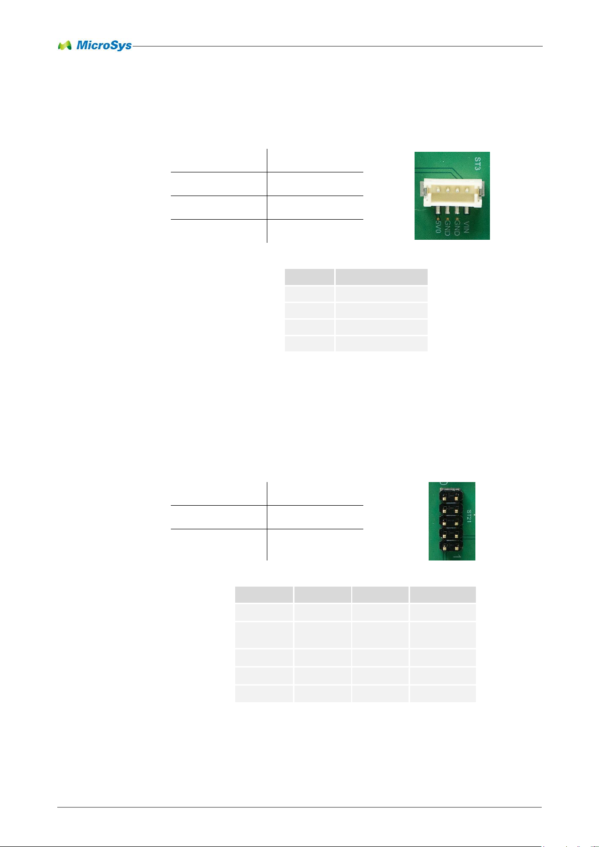
6.11 Fan Connector
The SBC-LS1028A provides a fan connector.
In case a fan is necessary MicroSys recommends to use a 5V rated fan.
Part Reference:
ST3
Manufacturer:
Würth Elektronik
Type:
679 304 124 022
Mates with:
648 004 113 322
Pin
Description
1
+5V
2
GND
3
GND
4
+VIN
Table 6-24 FAN connector pinout
6.12 Test Connector
Internal voltages are routed to a 10-pin 2.54mm pitch header to be measured
during production test.
Part Reference:
ST21
Manufacturer:
Würth Elektronik
Type:
61301021121
Description
Pin
Pin
Description
GND 1 2
VIN
3,3V 3 4
5V0_MODULE
1,8V 5 6
5V0
1,5V 7 8
VCC_RTC
1,0V 9 10
GND
Table 6-25 Test connector pinout
Switches, Buttons and Jumpers 7
miriac SBC-LS1028A User Manual
V 1.0
54/65
© MicroSys Electronics GmbH 2019
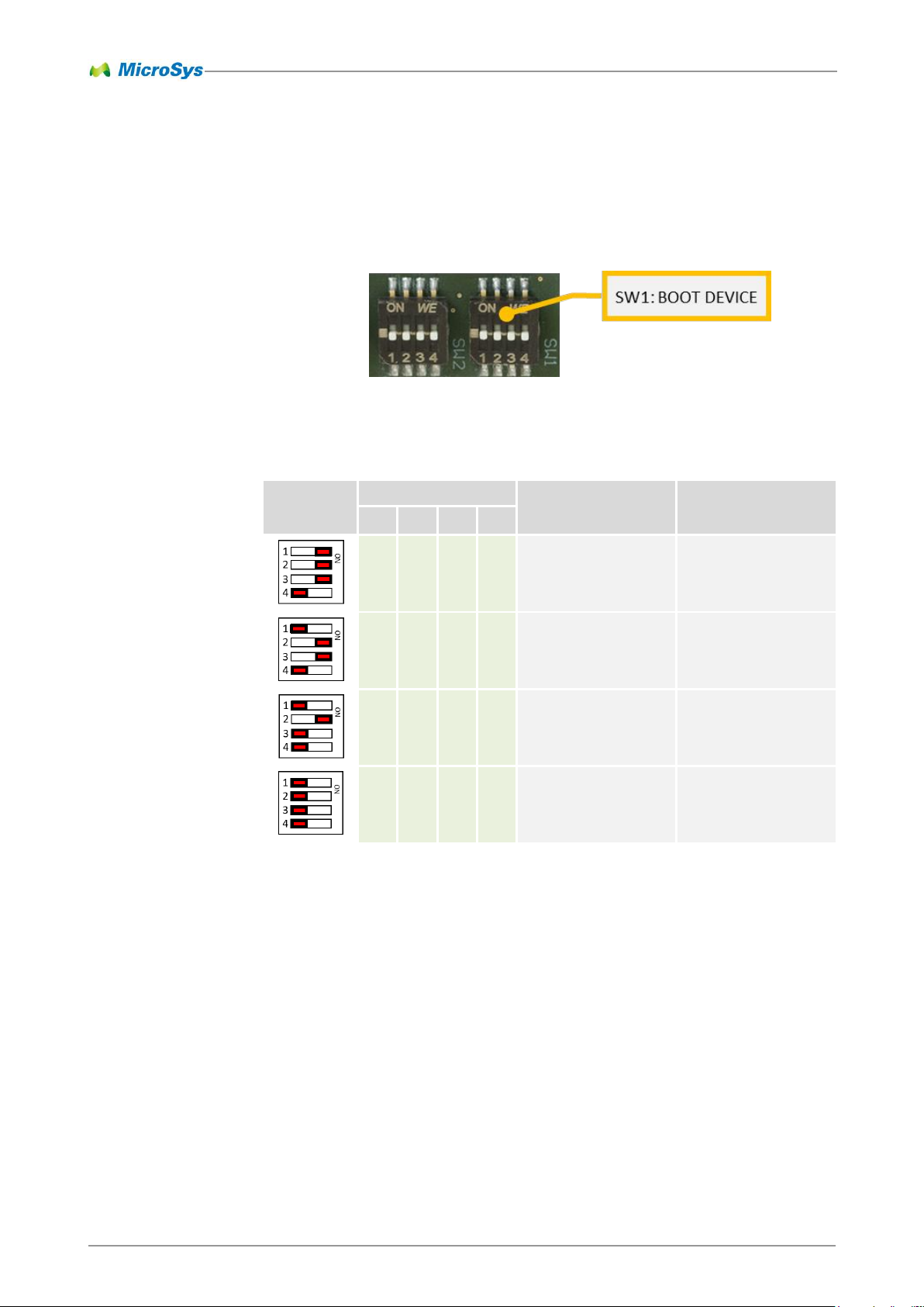
7 Switches, Buttons and Jumpers
7.1 Boot Device Switch
The boot device can be selected by means of switch “SW1”.
The following boot devices are supported by the SBC-LS1028A:
Setting
DIP Switch
Boot Source
Boot Device
Location
4
3 2 1
OFF
ON
ON
ON
SDHC1:
SD Card
carrier
OFF
ON
ON
OFF
SDHC2:
eMMC
carrier
OFF
OFF
ON
OFF
QSPI NAND Flash
(4KB pages)
module
OFF
OFF
OFF
OFF
QSPI NOR Flash
module
Figure 7-2 Boot device settings
Figure 7-1 Boot Device Switch

Switches, Buttons and Jumpers 7
miriac SBC-LS1028A User Manual
V 1.0
55/65
© MicroSys Electronics GmbH 2019
7.2 Board Configuration Switch
The following table lists the board configuration settings by switch “SW2:
Setting
DIP Switch
Description
4
3 2 1
x x x
ON
Not connected / unused
x
x
ON
x
ON: Boundary Scan enabled
OFF: Boundary Scan disabled
x
ON
x
x
ON: CPU module is PCIe Endpoint
OFF: CPU module is Root Complex (default)
ON
x x x
ON: mikroBUS reset is low active
OFF: mikroBUS reset is high active
Table 7-1 Configuration switch settings
Figure 7-3 Board Configuration Switch

Switches, Buttons and Jumpers 7
miriac SBC-LS1028A User Manual
V 1.0
56/65
© MicroSys Electronics GmbH 2019
7.3 Reset Button
Pressing the reset button “SW3” triggers a Hard Reset.
The reset button is connected to J6 and triggers the RSTIN# signal on ST6 pin
“T7”. See chapter 5.3 for more details.
Figure 7-4 Reset Button

LEDs 8
miriac SBC-LS1028A User Manual
V 1.0
57/65
© MicroSys Electronics GmbH 2019
8 LEDs
8.1 Power and Reset LEDs
Figure 8-1 LEDs on carrier
The LEDs are described from left to right:
Part
Refe-
rence
Colour
Source
Signal
Name
Function
LD3
RED
3V1_DP
OVC
Overcurrent on Displayport
ON: FAULT from J7
OFF = power to Displayport OK
LD5
RED
RSTIN#
RST
Reset active
ON if RSTIN# = low
OFF is RSTIN# = high
LD4
GREEN
5V0
5V0
Power 5,0V available
ON = 5V0 OK
OFF = 5V0 not available
LD6
GREEN
3V3_PGOOD
3V3
3,3V power good
ON = 3,3V OK
OFF = 3,3V not ok
LD7
GREEN
1V8
1V8
Power 1V8 available
ON = 1V8 OK
OFF = 1V8 not available
LD8
GREEN
1V5
1V5
Power 1V5 available
ON = 1V5 OK
OFF = 1V5 not available
LD9
GREEN
1V0
1V0
Power 1V0 available
ON = 1V0 OK
OFF = 1V0 not available
LD2
YELLOW
CFG_RCW2/GPO
GP1
ON = General Purpose Output is high
OFF = General Purpose Output is low
LD1
YELLOW
CFG_RCW3/GPO
GP0
ON = General Purpose Output is high
OFF = General Purpose Output is low
Table 8-1 Carrier Indicator LEDs

LEDs 8
miriac SBC-LS1028A User Manual
V 1.0
58/65
© MicroSys Electronics GmbH 2019
8.2 RJ45 LEDs
The following table summarizes the RJ45 LEDs of the SBC-LS1028A:
Part
Refe-
rence
Colour
Source
Signal Name
Function
Port 1
YELLOW
J15-E2
QSGMII_P0_LED1
LED on: Link
Port 1
GREEN
J15-D1
QSGMII_P0_LED0
LED blinking: Activity
Port 2
YELLOW
J15-G2
QSGMII_P1_LED1
LED on: Link
Port 2
GREEN
J15-F1
QSGMII_P1_LED0
LED blinking: Activity
Port 3
YELLOW
J15-J1
QSGMII_P2_LED1
LED on: Link
Port 3
GREEN
J15-H2
QSGMII_P2_LED0
LED blinking: Activity
Port 4
YELLOW
J15-L2
QSGMII_P3_LED1
LED on: Link
Port 4
GREEN
J15-L1
QSGMII_P3_LED0
LED blinking: Activity
SGMII
YELLOW
J17-13
SGMII_P0_LED1
LED on: Link
SGMII
GREEN
J17-14
SGMII_P0_LED0
LED blinking: Activity
RGMII
YELLOW
J18-13
RGMII_P0_LED1
LED on: Link
RGMII
GREEN
J18-14
RGMII_P0_LED0
LED blinking: Activity
Table 8-2 LAN Indicator LEDs
Figure 8-2 RJ45 LEDs

LEDs 8
miriac SBC-LS1028A User Manual
V 1.0
59/65
© MicroSys Electronics GmbH 2019
8.3 LEDs on MPX-LS1028A
Figure 8-3 LEDs on MPX-LS1028A
Part
Reference
Function
LD1
green
Power good
ON = power supplies are ok
OFF = power fail
LD2
red
Reset on Module
ON = active reset
OFF = no reset, CPU is active
Table 8-3 LEDs on CPU module
LD1
LD2

Software 9
miriac SBC-LS1028A User Manual
V 1.0
60/65
© MicroSys Electronics GmbH 2019
9 Software
9.1 U-Boot
The SBC-LS1028A uses U-Boot as the bootloader, which is always programmed in
both the board's QSPI NAND and QSPI NOR Flash memories on delivery.
Additionally, a U-Boot version is available for the microSD card.
Boot options can be selected by the Boot Device Switch (see chapter 7.1).
9.2 Operating System Support
MicroSys Electronics GmbH offers Linux and Microware's OS-9 RTOS support for
the board.
If you have ordered a Starter Kit, the most recent MicroSys Linux release will be
available on the accompanying microSD card, so you can start to develop and test
your application right away.

Known Issues 10
miriac SBC-LS1028A User Manual
V 1.0
61/65
© MicroSys Electronics GmbH 2019
10 Known Issues
The following features are currently not supported:
■ Boundary Scan has not been tested yet
■ PCIe Endpoint is currently not supported

Appendix 11
miriac SBC-LS1028A User Manual
V 1.0
62/65
© MicroSys Electronics GmbH 2019
11 Appendix
11.1 Acronyms
These acronyms are being used within the document; note that this list does not
claim to be complete or exhaustive:
CPU ............................................................................................... Central Processing Unit
DC ................................................................................................................. Direct Current
DDR4 ............................................................ Double Data Rate Memory fourth-generation
EC ......................................................................................................... Ethernet Controller
ESD ................................................................................................ Electrostatic Discharge
Gbps ...................................................................................................... Gigabit per second
GND ........................................................................................................................ Ground
GPL ................................................................................................ General Public License
JTAG .............................................................................................. Joint Test Action Group
LAN ...................................................................................................... Local Area Network
LED ..................................................................................................... Light Emitting Diode
LVTTL .................................................................. Low Voltage Transistor–Transistor Logic
MCU ..................................................................................................... Microcontroller Unit
MMC .......................................................................................................... Multimedia Card
mPCIe ................................................... Mini Peripheral Component Interconnect Express
mSATA ........................................................ Mini Serial Advanced Technology Attachment
RGMII ......................................................... Reduced Gigabit Media-independent Interface
RTC ........................................................................................................... Real Time Clock
SBC ................................................................................................ Single Board Computer
SD ................................................................................................................. Secure Digital
SDIO ......................................................................................... Secure Digital Input Output
SDRAM .................................................. Synchronous Dynamic Random Access Memory
SGMII .............................................................. Serial Gigabit Media-independent Interface
SOM ......................................................................................................System On Module
UART .......................................................... Universal Asynchronous Receiver Transmitter
USB ..................................................................................................... Universal Serial Bus

Appendix 11
miriac SBC-LS1028A User Manual
V 1.0
63/65
© MicroSys Electronics GmbH 2019
11.2 Table of Figures
Figure 3-1 System setup example ........................................................................................ 11
Figure 4-1 Block Diagram (MPX-LS1028A Rev. 2 on carrier CRX07 Rev. 2) ...................... 14
Figure 4-2 Mechanical Dimensions: Module ........................................................................ 16
Figure 4-3 Mechanical Dimensions: SBC-LS1028A Carrier ................................................. 17
Figure 4-4 Top connectors ................................................................................................... 18
Figure 4-5 Bottom connectors .............................................................................................. 19
Figure 4-6 Power supply structure ....................................................................................... 22
Figure 5-1 Reset Structure (carrier CRX07) ......................................................................... 25
Figure 5-2 Clock distribution................................................................................................. 27
Figure 5-3 Multiplexer I2C-1 bus .......................................................................................... 31
Figure 5-4 I2C-1 bus topology .............................................................................................. 31
Figure 6-1 SGMII topology ................................................................................................... 34
Figure 6-2 RGMII topology ................................................................................................... 35
Figure 6-3 QSGMII topology ................................................................................................ 36
Figure 6-4 SDHC1 topology ................................................................................................. 42
Figure 6-5 USB1 topology .................................................................................................... 44
Figure 6-6 USB2 topology .................................................................................................... 45
Figure 6-7 USB3 topology .................................................................................................... 46
Figure 6-8 DisplayPort topology ........................................................................................... 47
Figure 6-9 CAN1 topology .................................................................................................... 48
Figure 6-10 CAN2 topology .................................................................................................. 48
Figure 6-11 mikroBUS™ topology ........................................................................................ 49
Figure 7-1 Boot Device Switch ............................................................................................. 54
Figure 7-2 Boot device settings ............................................................................................ 54
Figure 7-3 Board Configuration Switch ................................................................................ 55
Figure 7-4 Reset Button ....................................................................................................... 56
Figure 8-1 LEDs on carrier ................................................................................................... 57
Figure 8-2 RJ45 LEDs .......................................................................................................... 58
Figure 8-3 LEDs on MPX-LS1028A ..................................................................................... 59

Appendix 11
miriac SBC-LS1028A User Manual
V 1.0
64/65
© MicroSys Electronics GmbH 2019
11.3 Table of Tables
Table 1-1 Symbols ................................................................................................................. 6
Table 1-2 Conventions ........................................................................................................... 6
Table 2-1 Functional coverage ............................................................................................... 9
Table 4-1 Pinout Pressure Clamp ........................................................................................ 21
Table 4-2 Pinout Power Jack ............................................................................................... 21
Table 4-3 Voltage monitoring limits (carrier)......................................................................... 23
Table 5-1 Reset signal overview .......................................................................................... 25
Table 5-2 Hard-wired boot signals ....................................................................................... 28
Table 5-3 QSPI Serial NAND Flash pin assignments ........................................................... 29
Table 5-4 QSPI NOR Flash pin assignment ......................................................................... 30
Table 5-5 I²C-1 bus map ...................................................................................................... 31
Table 6-1 Connector reference overview ............................................................................. 32
Table 6-2 LAN / DTSEC / SerDes / RGMII assignment ....................................................... 33
Table 6-3 LAN Gigabit Ethernet connector pairs .................................................................. 34
Table 6-4 SerDes 0 pin assignment ..................................................................................... 34
Table 6-5 Port RGMII pin assignment .................................................................................. 35
Table 6-6 SerDes 1 pin assignment ..................................................................................... 36
Table 6-7 PCIe SerDes assignment ..................................................................................... 37
Table 6-8 mPCIe Slot pinout ................................................................................................ 38
Table 6-9 mPCIe Slot SerDes 2 assignment ........................................................................ 38
Table 6-10 mPCIe / mSATA Slot pinout ............................................................................... 40
Table 6-11 mPCIe Slot SerDes 3 assignment ...................................................................... 40
Table 6-12 PCIe Root Complex / Endpoint .......................................................................... 41
Table 6-13 microSD card slot pin assignment ...................................................................... 42
Table 6-14 USB Host-Only Port 1 pin assignment ............................................................... 43
Table 6-15 USB Host-Only Port 2 pin assignment ............................................................... 45
Table 6-16 USB Host-Only Port 3 pin assignment ............................................................... 46
Table 6-17 DisplayPort Connector Pinout ............................................................................ 47
Table 6-18 CAN1 pin assignment ST1 ................................................................................. 48
Table 6-19 CAN2 pin assignment ST2 ................................................................................. 48
Table 6-20 mikroBUS™ pin assignment ST15 ..................................................................... 50
Table 6-21 mikroBUS™ pin assignment ST16 ..................................................................... 50
Table 6-22 JTAG connector pinout to module ...................................................................... 51
Table 6-23 JTAG Connector Pinout carrier .......................................................................... 52
Table 6-24 FAN connector pinout ........................................................................................ 53
Table 6-25 Test connector pinout ......................................................................................... 53
Table 7-1 Configuration switch settings ............................................................................... 55
Table 8-1 Carrier Indicator LEDs .......................................................................................... 57
Table 8-2 LAN Indicator LEDs .............................................................................................. 58
Table 8-3 LEDs on CPU module .......................................................................................... 59
Table 12-1 Document history ............................................................................................... 65

History 12
miriac SBC-LS1028A User Manual
V 1.0
65/65
© MicroSys Electronics GmbH 2019
12 History
Date
Version
Change Description
2019-09-11
1.0
First Release
Table 12-1 Document history
 Loading...